Measuring and modelling the mechanical stress transmitted by Silicon Nitride lines on Silicon substrates
|
|
|
- Owen Terence McCormick
- 5 years ago
- Views:
Transcription


1 Measuring and modelling the mechanical stress transmitted by Silicon Nitride lines on Silicon substrates P. Benzo, S. Reboh, M. J. Hÿtch, S. Schamm-Chardon, R. Cours and A. Claverie Groupe nmat, CEMES-CNRS et Université de Toulouse P. Morin, A. Halimaoui, D. Bensahel ST Microelectronics, Crolles GDR - Mecano Poitiers 8 Avril 2011
2 Outline - Strain engineering in MOSFET devices - Interest of Silicon Nitride lines arrays - Strain mapping by Electron Holography - Results - Scalability issues - Conclusions and perspectives


 Stress enhance")
3 Strain engineering in MOSFET devices MOSFET Transistor J. Huang et al. Thin solid films 518 (2010) Stress enhance charge mobility in MOSFET devices
 Silicon Nitride liner Stress transmission mechanism not clear Understand the stress transmission mechanism from stressed SiN liner to Si")
4 Strain engineering in MOSFET devices 3 different approaches: 1) SiGe buried substrate 2) SiGe Source and Drain Stress transmission mechanism well understood Mark Bohr, Intel ) Silicon Nitride liner Stress transmission mechanism not clear Understand the stress transmission mechanism from stressed SiN liner to Si substrate

5 Why Silicon Nitride liners - SiN in MOSFET as capping etch-stopping layer (CESL) - SiN tensile or compressive based on deposition method => PMOS / NMOS Study: - local stress - influence of processing parameters Preliminary study difficult because: - SiN dependence on deposition parameters - Bidimensional MOSFET geometry Need a simpler system - Different materials involved

 (wafer bending) - nominal Young s modulus SiN = 160 GPa")
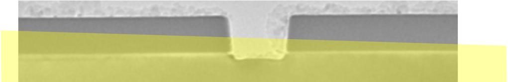
: - Lines length L = 1 µm - Lines Height T SiN")
6 Analyzed Structure Strained Silicon Nitride arrays on Silicon substrate SiN SiN SiN Physical properties: - SiN => PECVD + e-beam lithography Si <100> - nominal stress SiN = +1.2GPa biaxial (x,y) (wafer bending) - nominal Young s modulus SiN = 160 GPa - Substrate orientation: <100> T SiN L Tripod specimen preparation S L1 S0.14 Geometric properties (TEM): - Lines length L = 1 µm - Lines Height T SiN = 75 nm - Distance between lines S = µm


7 Stress transmission mechanism Free SiN film UV SiN H Volume reduction: Hydrogen expulsion Si-Si and Si-N bonding SiN film on a Silicon substrate SiN Si Bulk prevent volume reduction of SiN: - Compressive stresses in x and y - Tensile stress in z

")
8 Methods: TEM Dark Field Holography (HoloDark) Finite Element Method (FEM) simulations FEI Tecnai 20 Objectives: - Calibrate simulations with experiments for simple structures. - Use simulations to: - Calculate stresses distribution in bulk (non-relaxed) samples - Predict stresses distribution in more complicated structures


9 Dark-Field Electron Holography (DFEH) Spatial resolution: 2-4 nm Field of view: 500nm x 2µm Precision: few 10-4 M.J.Hÿtch, F.Houdellier, F.Hüe and E.Snoeck, Nature (2008) M.J.Hÿtch, F.Houdellier, F.Hüe, E.Snoeck, French Patent Application FR N


10 Dark-Field Electron Holography (DFEH) Experiment
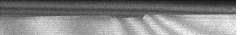
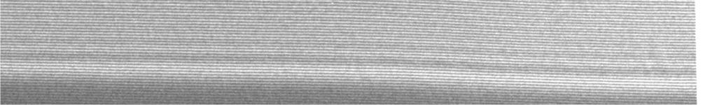
11 Dark-Field Electron Holography (DFEH) Experiment π φ g G -π

 2D")

![[2 0-2] 1 u(](/docs-images/82/86789635/images/12-3.jpg "r) = 1 1 g 2 )")


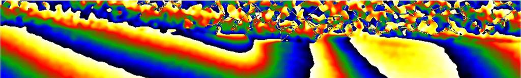
12 Dark-Field Electron Holography (DFEH) 2D Deformation g 1 [-2 0-2] g 2 [2 0-2] 1 u( r) = 1 1 g 2 ) a 2π [ ( r) a ( r ] G G φ g + φ 2 HoloDark 1.0 (HREM Research) by M. J. Hÿtch, C. Gatel & K. Ishizuka

 Strain")

 100 nm 100")
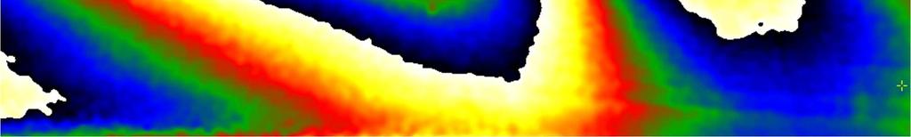
 Rotation")
13 Dark-Field Electron Holography (DFEH) Strain components Strain x (ε xx ) Strain z (ε zz ) 100 nm 100 nm Strain xz (ε xz ) Rotation xz (ω xz ) 100 nm 100 nm
 Simulations before thinning process Comparison Simulations")

14 Finite Elements Method TEM measurements are performed on thin specimen ( nm) Simulations before thinning process Comparison Simulations must take stress relaxation in thinning direction into account Validation relaxation Bulk Strain and stress mapping in whole bulk structure thin sample
 Symmetry planes Bulk")

15 Finite Elements Method Biaxial (x and y) initial stress 3D Simulations: SiN SiN SiN Thin sample (relaxed in y direction) Symmetry planes Bulk (non-relaxed) structure Variables: Anisotropic single-crystal Si Silicon Nitride initial stress: σ i z direction prescribed displacement Silicon Nitride Young s modulus: E
16 Results

17 Lines L1 S0.25 Simulations with σ i =1.2 GPa and E=160 GPa Simulation Vs Experiment Strain x Strain z HoloDark FEM

18 Lines L1 S0.25 Simulations with σ i =1.2 GPa and E=160 GPa Strain x Strain z Simulations results too high when compared to experiment Initial stress σ i too high Young s modulus too small
 400 350 300 250 200 150")
19 Lines L1 S0.25 Simulations with σ i =1.2 GPa and E=300 GPa Strain x Strain z Different couples of σ and E to reproduce experimental results Young's modulus (GPa) Initial stress (GPa) In literature: 160GPa < E SiN < 380GPa 0.95GPa < σ SiN < 1.35GPa


20 Lines L1 S0.14 Simulations with σ i =1.2 GPa and E=300 GPa Strain x Strain z Simulations in good agreement with experiment also for S=140nm Simulations are calibrated on thin specimens
21 Calculated strain in Bulk structures Lines L1 S0.25 Simulations with σ i =1.2 GPa and E=300 GPa Strain in bulk structure ~15% higher than in thin sample
 8x10 8 6x10 8 4x10 8 2x10 8 0 S = 16 nm S = 32 nm S = 70 nm S = 140 nm S = 250 nm Stress y Horizontal profile -4.")
22 Stresses in bulk structure How much scalable is our system? x stress Stress profile in the channel equivalent region Stress xx (Pa) 1.6x10 9 S = 16 nm 1.2x10 9 S = 32 nm S = 70 nm S = 140 nm 8.0x10 8 S = 250 nm 4.0x Stress x Horizontal profile Stress yy (Pa) 8x10 8 6x10 8 4x10 8 2x S = 16 nm S = 32 nm S = 70 nm S = 140 nm S = 250 nm Stress y Horizontal profile -4.0x Distance (nm) x stress saturates for S<32nm -2x Distance (nm) y stress increases also for S<32nm
23 Conclusions - HoloDark can measure strains under the SiN lines arrays with high precision. - To simulate our experimental results different couples of values of σ i and E can be used for SiN. - If the SiN stress (measured by wafer bending) is correct (1.2GPa) our results show that SiN Young s modulus is equal to 300GPa. Variation on Young s modulus observed in literature maybe due to deposition conditions. - Stress of channel equivalent region increases in y direction when line distance (S) decreases down to 16nm. - Stress of channel equivalent region saturates in x direction if S<32 nm.
24 Work in progress and perspectives - Study the effect of SiN lines geometry on stress distribution (different lines length are under analysis). - Study the effect of SiN liners on more complex geometries (MOSFET geometry) to understand how the shape influences stress distribution. - Study real MOSFET devices.


25 Acknowledgements UTTERMOST : UlTimaTe Enablement Research on 32/28nm cmos Technologies (01/ /2012) MINEFI : MINistère de l Ecomomie des Finances et de l Industrie Convention de Thèse CIFRE : Convention Industrielle de Formation par la REcherche (11/ /2012)
26
Materials Characterization for Stress Management
 Materials Characterization for Stress Management Ehrenfried Zschech, Fraunhofer IZFP Dresden, Germany Workshop on Stress Management for 3D ICs using TSVs San Francisco/CA, July 13, 2010 Outline Stress
Strain Engineering for Performance Enhancement in Advanced Nano Scaled SOI-MOSFETs
 Strain Engineering for Performance Enhancement in Advanced Nano Scaled SOI-MOSFETs S. Flachowsky a), R. Illgen a), T. Herrmann a), A. Wei b), J. Höntschel b), M. Horstmann b), W. Klix a), and R. Stenzel
Micro-Electro-Mechanical Systems (MEMS) Fabrication. Special Process Modules for MEMS. Principle of Sensing and Actuation
 Fabrication. Special Process Modules for MEMS. Principle of Sensing and Actuation") Micro-Electro-Mechanical Systems (MEMS) Fabrication Fabrication Considerations Stress-Strain, Thin-film Stress, Stiction Special Process Modules for MEMS Bonding, Cavity Sealing, Deep RIE, Spatial forming
Micro-Electro-Mechanical Systems (MEMS) Fabrication Fabrication Considerations Stress-Strain, Thin-film Stress, Stiction Special Process Modules for MEMS Bonding, Cavity Sealing, Deep RIE, Spatial forming
MEMS 487. Class 04, Feb. 13, K.J. Hemker
 MEMS 487 Class 04, Feb. 13, 2003 Materials Come As:!Amorphous Glasses, polymers, some metal alloys Processing can result in amorphous structures! Crystalline Single crystals Textured crystals Polycrystalline
Tri-Gate Transistor Architecture with High-k Gate Dielectrics, Metal Gates and Strain Engineering
 Tri-Gate Transistor Architecture with High-k Gate Dielectrics, Metal Gates and Strain Engineering Jack Kavalieros, Brian Doyle, Suman Datta, Gilbert Dewey, Mark Doczy, Ben Jin, Dan Lionberger, Matthew
Piezoresistance in Silicon. Dr. Lynn Fuller Webpage:
 ROCHESTER INSTITUTE OF TECHNOLOGY MICROELECTRONIC ENGINEERING Piezoresistance in Silicon Webpage: http://people.rit.edu/lffeee 82 Lomb Memorial Drive Rochester, NY 14623-5604 Tel (585) 475-2035 Email:
Layout-related stress effects on TID-induced leakage current
 Layout-related stress effects on TID-induced leakage current Nadia Rezzak, R. D. Schrimpf, M. L. Alles, En Xia Zhang, Daniel M. Fleetwood, Yanfeng Albert Li Radiation Effects Group Vanderbilt University,
Micro-Electro-Mechanical Systems (MEMS) Fabrication. Special Process Modules for MEMS. Principle of Sensing and Actuation
 Fabrication. Special Process Modules for MEMS. Principle of Sensing and Actuation") Micro-Electro-Mechanical Systems (MEMS) Fabrication Fabrication Considerations Stress-Strain, Thin-film Stress, Stiction Special Process Modules for MEMS Bonding, Cavity Sealing, Deep RIE, Spatial forming
Micro-Electro-Mechanical Systems (MEMS) Fabrication Fabrication Considerations Stress-Strain, Thin-film Stress, Stiction Special Process Modules for MEMS Bonding, Cavity Sealing, Deep RIE, Spatial forming
NANOINDENTATION OF SILICON CARBIDE WAFER COATINGS
 NANOINDENTATION OF SILICON CARBIDE WAFER COATINGS Prepared by Jesse Angle 6 Morgan, Ste156, Irvine CA 9618 P: 949.461.99 F: 949.461.93 nanovea.com Today's standard for tomorrow's materials. 010 NANOVEA
Micro-Electro-Mechanical Systems (MEMS) Fabrication. Special Process Modules for MEMS. Principle of Sensing and Actuation
 Fabrication. Special Process Modules for MEMS. Principle of Sensing and Actuation") Micro-Electro-Mechanical Systems (MEMS) Fabrication Fabrication Considerations Stress-Strain, Thin-film Stress, Stiction Special Process Modules for MEMS Bonding, Cavity Sealing, Deep RIE, Spatial forming
Micro-Electro-Mechanical Systems (MEMS) Fabrication Fabrication Considerations Stress-Strain, Thin-film Stress, Stiction Special Process Modules for MEMS Bonding, Cavity Sealing, Deep RIE, Spatial forming
Lect. 2: Basics of Si Technology
 Unit processes Thin Film Deposition Etching Ion Implantation Photolithography Chemical Mechanical Polishing 1. Thin Film Deposition Layer of materials ranging from fractions of nanometer to several micro-meters
Performance Predictions for Scaled Process-induced Strained-Si CMOS
 Performance Predictions for Scaled Process-induced Strained-Si CMOS G Ranganayakulu and C K Maiti Department of Electronics and ECE, IIT Kharagpur, Kharagpur 721302, India Abstract: Device and circuit
Piezoresistance in Silicon. Dr. Lynn Fuller
 ROCHESTER INSTITUTE OF TECHNOLOGY MICROELECTRONIC ENGINEERING in Silicon Dr. Lynn Fuller Webpage: http://people.rit.edu/lffeee 82 Lomb Memorial Drive Rochester, NY 14623-5604 Tel (585) 475-2035 Fax (585)
UT Austin, ECE Department VLSI Design 2. CMOS Fabrication, Layout Rules
 2. CMOS Fabrication, Layout, Design Rules Last module: Introduction to the course How a transistor works CMOS transistors This module: CMOS Fabrication Design Rules CMOS Fabrication CMOS transistors are
Thin Film Scattering: Epitaxial Layers
 Thin Film Scattering: Epitaxial Layers 6th Annual SSRL Workshop on Synchrotron X-ray Scattering Techniques in Materials and Environmental Sciences: Theory and Application May 29-31, 2012 Thin films. Epitaxial
JJMIE Jordan Journal of Mechanical and Industrial Engineering
 JJMIE Jordan Journal of Mechanical and Industrial Engineering Volume 5, Number 6, Dec. 211 ISSN 1995-6665 Pages 553-557 On the Deformation Modes of Continuous Bending under Tension Test A. Hadoush*,a a
Problem 1 Lab Questions ( 20 points total)
") Problem 1 Lab Questions ( 20 points total) (a) (3 points ) In our EE143 lab, we use Phosphorus for the source and drain diffusion. However, most advanced processes use Arsenic. What is the advantage of
Problem 1 Lab Questions ( 20 points total) (a) (3 points ) In our EE143 lab, we use Phosphorus for the source and drain diffusion. However, most advanced processes use Arsenic. What is the advantage of
Complexity of IC Metallization. Early 21 st Century IC Technology
 EECS 42 Introduction to Digital Electronics Lecture # 25 Microfabrication Handout of This Lecture. Today: how are Integrated Circuits made? Silicon wafers Oxide formation by growth or deposition Other
Measurement of Residual Stress by X-ray Diffraction
 Measurement of Residual Stress by X-ray Diffraction C-563 Overview Definitions Origin Methods of determination of residual stresses Method of X-ray diffraction (details) References End Stress and Strain
Lecture 19 Microfabrication 4/1/03 Prof. Andy Neureuther
 EECS 40 Spring 2003 Lecture 19 Microfabrication 4/1/03 Prof. ndy Neureuther How are Integrated Circuits made? Silicon wafers Oxide formation by growth or deposition Other films Pattern transfer by lithography
Complementary Metal Oxide Semiconductor (CMOS)
") Technische Universität Graz Institute of Solid State Physics Complementary Metal Oxide Semiconductor (CMOS) Franssila: Chapters 26,28 Technische Universität Graz Institute of Solid State Physics Complementary
Technische Universität Graz Institute of Solid State Physics Complementary Metal Oxide Semiconductor (CMOS) Franssila: Chapters 26,28 Technische Universität Graz Institute of Solid State Physics Complementary
Review of CMOS Processing Technology
 - Scaling and Integration Moore s Law Unit processes Thin Film Deposition Etching Ion Implantation Photolithography Chemical Mechanical Polishing 1. Thin Film Deposition Layer of materials ranging from
Microfabrication of Integrated Circuits
 Microfabrication of Integrated Circuits OUTLINE History Basic Processes Implant; Oxidation; Photolithography; Masks Layout and Process Flow Device Cross Section Evolution Lecture 38, 12/05/05 Reading This
Packaging Effect on Reliability for Cu/Low k Damascene Structures*
 Packaging Effect on Reliability for Cu/Low k Damascene Structures* Guotao Wang and Paul S. Ho Laboratory of Interconnect & Packaging, TX 78712 * Work supported by SRC through the CAIST Program TRC 2003
Advanced CMOS Process Technology Part 3 Dr. Lynn Fuller
 MICROELECTRONIC ENGINEERING ROCHESTER INSTITUTE OF TECHNOLOGY Part 3 Dr. Lynn Fuller Webpage: http://people.rit.edu/lffeee Electrical and Microelectronic Engineering Rochester Institute of Technology 82
HONEYCOMB MECHANICAL BEHAVIOR USING MACROINDENTATION
 HONEYCOMB MECHANICAL BEHAVIOR USING MACROINDENTATION. Prepared by Duanjie Li, PhD 6 Morgan, Ste156, Irvine CA 92618 P: 949.461.9292 F: 949.461.9232 nanovea.com Today's standard for tomorrow's materials.
Strained Silicon-On-Insulator Fabrication and Characterization
 10.1149/1.2728880, The Electrochemical Society Strained Silicon-On-Insulator Fabrication and Characterization M. Reiche a, C. Himcinschi a, U. Gösele a, S. Christiansen a, S. Mantl b, D. Buca b, Q.T. Zhao
Manufacturer Part Number. Module 2: CMOS FEOL Analysis
 Manufacturer Part Number description Module 2: CMOS FEOL Analysis Manufacturer Device # 2 Some of the information is this report may be covered by patents, mask and/or copyright protection. This report
This Appendix discusses the main IC fabrication processes.
 IC Fabrication B B.1 Introduction This Appendix discusses the main IC fabrication processes. B.2 NMOS fabrication NMOS transistors are formed in a p-type substrate. The NMOS fabrication process requires
EXCIMER LASER ANNEALING FOR LOW- TEMPERATURE POLYSILICON THIN FILM TRANSISTOR FABRICATION ON PLASTIC SUBSTRATES
 EXCIMER LASER ANNEALING FOR LOW- TEMPERATURE POLYSILICON THIN FILM TRANSISTOR FABRICATION ON PLASTIC SUBSTRATES G. Fortunato, A. Pecora, L. Maiolo, M. Cuscunà, D. Simeone, A. Minotti, and L. Mariucci CNR-IMM,
CMOS Technology. Flow varies with process types & company. Start with substrate selection. N-Well CMOS Twin-Well CMOS STI
 CMOS Technology Flow varies with process types & company N-Well CMOS Twin-Well CMOS STI Start with substrate selection Type: n or p Doping level, resistivity Orientation, 100, or 101, etc Other parameters
Thin Film Scattering: Epitaxial Layers
 Thin Film Scattering: Epitaxial Layers Arturas Vailionis First Annual SSRL Workshop on Synchrotron X-ray Scattering Techniques in Materials and Environmental Sciences: Theory and Application Tuesday, May
Micro-tube insertion into aluminum pads: Simulation and experimental validations
 Micro-tube insertion into aluminum pads: Simulation and experimental validations A. Bedoin, B. Goubault, F. Marion, M. Volpert, F. Berger, A. Gueugnot, H. Ribot CEA, LETI, Minatec Campus 17, rue des Martyrs
Low Temperature Dielectric Deposition for Via-Reveal Passivation.
 EMPC 2013, September 9-12, Grenoble; France Low Temperature Dielectric Deposition for Via-Reveal Passivation. Kath Crook, Mark Carruthers, Daniel Archard, Steve Burgess, Keith Buchanan SPTS Technologies,
EE-612: Lecture 28: Overview of SOI Technology
 EE-612: Lecture 28: Overview of SOI Technology Mark Lundstrom Electrical and Computer Engineering Purdue University West Lafayette, IN USA Fall 2006 NCN www.nanohub.org Lundstrom EE-612 F06 1 outline 1)
VLSI Digital Systems Design
 VLSI Digital Systems Design CMOS Processing cmpe222_03process_ppt.ppt 1 Si Purification Chemical purification of Si Zone refined Induction furnace Si ingot melted in localized zone Molten zone moved from
T. Ben Britton.
 T. Ben Britton b.britton@imperial.ac.uk / @BMatB http://expmicromech.com Acknowledgments: Angus Wilkinson, Angus Kirkland, Fionn Dunne, Jun Jiang, Vivian Tong, David Wallis, Lars Hansen, Aimo Winkelmann
X-ray optical thin film deposition and analysis capability at NASA MSFC. D. Broadway. 11/8/2017 D. Broadway NASA MSFC 1
 X-ray optical thin film deposition and analysis capability at ASA MSFC D. Broadway /8/7 D. Broadway ASA MSFC Talk Outline Optical thin film coating capability at MSFC Deposition system X-ray reflectometer
Materials Characterization
 Materials Characterization C. R. Abernathy, B. Gila, K. Jones Cathodoluminescence (CL) system FEI Nova NanoSEM (FEG source) with: EDAX Apollo silicon drift detector (TE cooled) Gatan MonoCL3+ FEI SEM arrived
Thermo-Mechanical Reliability of Through-Silicon Vias (TSVs)
") 1 Thermo-Mechanical Reliability of Through-Silicon Vias (TSVs) Xi Liu Ph.D. Student and Suresh K. Sitaraman, Ph.D. Professor The George W. Woodruff School of Mechanical Engineering Georgia Institute of
1 Thermo-Mechanical Reliability of Through-Silicon Vias (TSVs) Xi Liu Ph.D. Student and Suresh K. Sitaraman, Ph.D. Professor The George W. Woodruff School of Mechanical Engineering Georgia Institute of
Introduction to CMOS VLSI Design. Layout, Fabrication, and Elementary Logic Design
 Introduction to CMOS VLSI Design Layout, Fabrication, and Elementary Logic Design CMOS Fabrication CMOS transistors are fabricated on silicon wafer Lithography process similar to printing press On each
Effects of Film Thickness on the Yielding Behavior of Polycrystalline Gold Films
 Effects of Film Thickness on the Yielding Behavior of Polycrystalline Gold Films H.D. Espinosa and B.C. Prorok Department of Mechanical Engineering, Northwestern University Evanston, IL 628-3111, USA ABSTRACT
EFFECT OF BODY GEOMETRY AND MATERIAL PROPERTIES ON RESIDUAL STRESS DISTRIBUTION ON ARRESTING CRACK HOLES.
 EFFECT OF BODY GEOMETRY AND MATERIAL PROPERTIES ON RESIDUAL STRESS DISTRIBUTION ON ARRESTING CRACK HOLES. C. Rubio-González a, G. Mesmacque b, J. Santos-García b, A. Amrouche b a Centro de Ingeniería y
Silicon Stress Metrology for Cu-TSVs in 3D ICs
 Silicon Stress Metrology for Cu-TSVs in 3D ICs Colin McDonough, Benjamin Backes, Pratibha Singh, Larry Smith, Wei Wang, and Robert E. Geer College of Nanoscale Science & Engineering, University at Albany,
FIBRE-COUPLED HIGH-INDEX PECVD SILICON- OXYNITRIDE WAVEGUIDES ON SILICON
 FIBRE-COUPLED HIGH-INDEX PECVD SILICON- OXYNITRIDE WAVEGUIDES ON SILICON Maxim Fadel and Edgar Voges University of Dortmund, High Frequency Institute, Friedrich-Woehler Weg 4, 44227 Dortmund, Germany ABSTRACT
Supporting Information
 Supporting Information Dislocations Accelerate Oxygen Ion Diffusion in La 0.8 Sr 0.2 MnO 3 Epitaxial Thin Films Edvinas Navickas 1, Yan Chen 2χ, Qiyang Lu 3, Wolfgang Wallisch 4, Tobias M. Huber 1,2,3,5,6,
EXPERIMENTAL STUDY OF THE STRESS RELIEF IN PATCHED ALUMINIUM SPECIMENS
 EXPERIMENTAL STUDY OF THE STRESS RELIEF IN PATCHED ALUMINIUM SPECIMENS Marie-Pierre Moutrille, Xavier Balandraud, Michel Grédiac Laboratoire de Mécanique et Ingénierie (LaMI) Blaise Pascal University (UBP),
EE40 Lec 22. IC Fabrication Technology. Prof. Nathan Cheung 11/19/2009
 Suggested Reading EE40 Lec 22 IC Fabrication Technology Prof. Nathan Cheung 11/19/2009 300mm Fab Tour http://www-03.ibm.com/technology/manufacturing/technology_tour_300mm_foundry.html Overview of IC Technology
Kinematical theory of contrast
 Kinematical theory of contrast Image interpretation in the EM the known distribution of the direct and/or diffracted beam on the lower surface of the crystal The image on the screen of an EM = the enlarged
Notch fatigue resistance of shot peened high-strength aluminium alloys: The role of residual stress relaxation
 UNIVERSITÀ DI PISA Notch fatigue resistance of shot peened high-strength aluminium alloys: 1, V. Fontanari 1, C. Santus 2 1 Department of Materials Engineering and Industrial Technologies, University of
A Combined Discrete-dislocation/Scaledependent Crystal Plasticity Analysis of Deformation and Fracture in Nanomaterials. Presented by: Derek Columbus
 MS Thesis Defense A Combined Discrete-dislocation/Scaledependent Crystal Plasticity Analysis of Deformation and Fracture in Nanomaterials Presented by: Derek Columbus Advisor: Dr. Mica Grujicic Department
THREE-DIMENSIONAL ELECTRONIC SURFACES
 THREE-DIMENSIONAL ELECTRONIC SURFACES PAI-HUI IRIS HSU A DISSERTATION PRESENTED TO THE FACULTY OF PRINCETON UNIVERSITY IN CANDIDACY FOR THE DEGREE OF DOCTOR OF PHILOSOPHY RECOMMENDED FOR ACCEPTANCE BY
Chapter 3 Silicon Device Fabrication Technology
 Chapter 3 Silicon Device Fabrication Technology Over 10 15 transistors (or 100,000 for every person in the world) are manufactured every year. VLSI (Very Large Scale Integration) ULSI (Ultra Large Scale
Behavior of the parameters of microcrystalline silicon TFTs under mechanical strain. S. Janfaoui*, C. Simon, N. Coulon, T.
 Author manuscript, published in "Solid-State Electronics 93 (2014) 1-7" DOI : 10.1016/j.sse.2013.12.001 Behavior of the parameters of microcrystalline silicon TFTs under mechanical strain S. Janfaoui*,
A diffused silicon pressure transducer with stress concentrated at transverse gages. Technical paper 267
 A diffused silicon pressure transducer with stress concentrated at transverse gages Technical paper 267 A diffused silicon pressure transducer with stress concentrated at transverse gages Many Meggitt
Scanning Electron Microscope & Surface Analysis. Wageningen EM Centre Marcel Giesbers
 Scanning Electron Microscope & Surface Analysis Wageningen EM Centre Marcel Giesbers Scanning Electron Microscope & Surface Analysis SEM vs Light Microscope and Transmission EM Secondary Electron Imaging
5.8 Diaphragm Uniaxial Optical Accelerometer
 5.8 Diaphragm Uniaxial Optical Accelerometer Optical accelerometers are based on the BESOI (Bond and Etch back Silicon On Insulator) wafers, supplied by Shin-Etsu with (100) orientation, 4 diameter and
Effects of Thin Film Depositions on the EUV mask Flatness
 Effects of Thin Film Depositions on the EUV mask Flatness Kyoung-Yoon Bang, Jinback Back, Hwan-Seok Seo, Dongwan Kim, DongHoon Chung, SeongSue Kim, Sang-Gyun Woo, and HanKu Cho Photomask Team Semiconductor
Lecture 2: CMOS Fabrication Mark McDermott Electrical and Computer Engineering The University of Texas at Austin
 Lecture 2: CMOS Fabrication Mark McDermott Electrical and Computer Engineering The University of Texas at Austin Agenda Last module: Introduction to the course How a transistor works CMOS transistors This
Experimental and numerical studies of axial compressive behaviour of slender I-section column
 Experimental and numerical studies of axial compressive behaviour of slender I-section column R. Muruganantham 1, J. Jeyanthi 2, G.Janani 3 1 P.G student, Department of civil Engineering, Mepco Schlenk
Strain for CMOS performance Improvement
 IBM Corporation Strain for CMOS performance Improvement +Victor Chan, +Ken Rim, #Meikei Ieong, +Sam Yang, +Rajeev Malik, Young Way Teh, #Min Yang, #Qiqing (Christine) Ouyang +IBM Systems & Technology Group,
FABRICATION of MOSFETs
 FABRICATION of MOSFETs CMOS fabrication sequence -p-type silicon substrate wafer -creation of n-well regions for pmos transistors, -impurity implantation into the substrate. -thick oxide is grown in the
Schottky-Barrier-Height Modulation of Ni Silicide/Si Contacts by Insertion of Thin Er or Pt Layers
 Schottky-Barrier-Height Modulation of Ni Silicide/Si Contacts by Insertion of Thin Er or Pt Layers Yoshihisa Ohishi 1, Kohei Noguchi 1, Kuniyuki Kakushima 2, Parhat Ahmet 1, Kazuo Tsutsui 2, Nobuyuki Sugii
Through Silicon Vias Annealing: A thermo-mechanical assessment
 Dresden University of Technology / Through Silicon Vias Annealing: P. Saettler (1), K. J. Wolter (1), M. Hecker (2), M. Boettcher (3) and C. Rudolph (3) (1) Technische Universität Dresden, (2) Globalfoundries
FABRICATION OF CMOS INTEGRATED CIRCUITS. Dr. Mohammed M. Farag
 FABRICATION OF CMOS INTEGRATED CIRCUITS Dr. Mohammed M. Farag Outline Overview of CMOS Fabrication Processes The CMOS Fabrication Process Flow Design Rules EE 432 VLSI Modeling and Design 2 CMOS Fabrication
Latching Shape Memory Alloy Microactuator
 Latching Shape Memory Alloy Microactuator ENMA490, Fall 00 S. Cabrera, N. Harrison, D. Lunking, R. Tang, C. Ziegler, T. Valentine Outline Background Problem Project Development Design Evaluation Applications
Chapter 3 CMOS processing technology
 Chapter 3 CMOS processing technology (How to make a CMOS?) Si + impurity acceptors(p-type) donors (n-type) p-type + n-type => pn junction (I-V) 3.1.1 (Wafer) Wafer = A disk of silicon (0.25 mm - 1 mm thick),
In-situ nano-mechanical tests in the light of μlaue diffraction
 Engineering Conferences International ECI Digital Archives Nanomechanical Testing in Materials Research and Development V Proceedings Fall 10-8-2015 In-situ nano-mechanical tests in the light of μlaue
Examples of dry etching and plasma deposition at Glasgow University
 Examples of dry etching and plasma deposition at Glasgow University Glasgow has pioneered and established many novel research activities involving the development of new dry etch processes and dry etch
Manufacturing Process
 Manufacturing Process 1 CMOS Process 2 A Modern CMOS Process gate-oxide TiSi 2 AlCu Tungsten SiO 2 n+ p-well p-epi poly n-well p+ SiO 2 p+ Dual-Well Trench-Isolated CMOS Process 3 Single-crystal ingot
Modeling of friction and structural transformations in diamond-like carbon coatings
 Modeling of friction and structural transformations in diamond-like carbon coatings Multiscale modelling and design for engineering applications VTT, Espoo, 5 th of February, 2013 H. Ronkainen, A. Laukkanen,
EE C245 ME C218 Introduction to MEMS Design Fall 2011
 Lecture Outline EE C245 ME C218 Introduction to MEMS Design Fall 2011 Prof. Clark T.-C. Nguyen Dept. of Electrical Engineering & Computer Sciences University of California at Berkeley Berkeley, CA 94720
6.774 Fall 2006: Global and Local Stress to Enhance CMOS Performance
 6.774 Fall 2006: Global and Local Stress to Enhance CMOS Performance techniques have been developed to strain the Si in the MOSFET channel, in order to enhance carrier mobility and current drive some of
ECCI of AlGaN/GaN HEMT structures grown on Si
 ECCI of AlGaN/GaN HEMT structures grown on Si D. Thomson 1, G. Naresh-Kumar 1, B. Hourahine 1, C. Trager-Cowan 1, P. Wright 2 and T. Martin 2 1 Dept. Of Physics, SUPA, University of Strathclyde, Glasgow
8 Displacements near the Face of an Advancing Shaft
 Displacements near the Face of an Advancing Shaft 8-1 8 Displacements near the Face of an Advancing Shaft 8.1 Problem Statement A circular shaft is excavated in chalk and lined with monolithic precast
Lecture 5. SOI Micromachining. SOI MUMPs. SOI Micromachining. Silicon-on-Insulator Microstructures. Agenda:
 EEL6935 Advanced MEMS (Spring 2005) Instructor: Dr. Huikai Xie SOI Micromachining Agenda: SOI Micromachining SOI MUMPs Multi-level structures Lecture 5 Silicon-on-Insulator Microstructures Single-crystal
PROCESS FLOW AN INSIGHT INTO CMOS FABRICATION PROCESS
 Contents: VI Sem ECE 06EC63: Analog and Mixed Mode VLSI Design PROCESS FLOW AN INSIGHT INTO CMOS FABRICATION PROCESS 1. Introduction 2. CMOS Fabrication 3. Simplified View of Fabrication Process 3.1 Alternative
In situ TEM Characterization of Shear Stress-Induced Interlayer. Sliding in the Cross Section View of Molybdenum Disulfide
 In situ TEM Characterization of Shear Stress-Induced Interlayer Sliding in the Cross Section View of Molybdenum Disulfide Juan Pablo Oviedo, Santosh KC, Ning Lu, Jinguo Wang, Kyeongjae Cho, Robert M. Wallace,
Welcome MNT Conference 1 Albuquerque, NM - May 2010
 Welcome MNT Conference 1 Albuquerque, NM - May 2010 Introduction to Design Outline What is MEMs Design General Considerations Application Packaging Process Flow What s available Sandia SUMMiT Overview
High Performance High-K + Metal Gate Strain Enhanced Transistors on (110) Silicon
 Silicon") High Performance High-K + Metal Gate Strain Enhanced Transistors on (110) Silicon Paul Packan, S. Cea*, H. Deshpande, T. Ghani, M. Giles*, O. Golonzka, M. Hattendorf, R. Kotlyar*, K. Kuhn, A. Murthy, P.
High Performance High-K + Metal Gate Strain Enhanced Transistors on (110) Silicon Paul Packan, S. Cea*, H. Deshpande, T. Ghani, M. Giles*, O. Golonzka, M. Hattendorf, R. Kotlyar*, K. Kuhn, A. Murthy, P.
Supplementary Figures
 Supplementary Figures Supplementary Figure 1. (a) Transmittance spectra of the TCM at different strains as tested before the fatigue test; (b) correlation between cyclic stress and cycles curve for the
Universität Hamburg, Hamburg, Germany. Universität Hamburg, Hamburg, Germany
 Sample Preparation, Micromagnetic Simulations, Circular-Rotational Currents, Parasitic Oersted Fields and Clover Samples (Magnetic Antivortex-Core Reversal by Circular-Rotational Spin Currents) Thomas
Design and analysis of MEMS MWCNT/epoxy strain sensor using COMSOL
 Pramana J. Phys. (2017) 89:10 DOI 10.1007/s12043-017-1398-8 Indian Academy of Sciences Design and analysis of MEMS MWCNT/epoxy strain sensor using COMSOL GAURAV SAPRA and PREETIKA SHARMA UIET, Panjab University,
Lecture 030 Integrated Circuit Technology - I (5/8/03) Page 030-1
 Page 030-1") Lecture 030 Integrated Circuit Technology - I (5/8/03) Page 030-1 LECTURE 030 INTEGRATED CIRCUIT TECHNOLOGY - I (References [7,8]) Objective The objective of this presentation is: 1.) Illustrate integrated
Lecture 030 Integrated Circuit Technology - I (5/8/03) Page 030-1 LECTURE 030 INTEGRATED CIRCUIT TECHNOLOGY - I (References [7,8]) Objective The objective of this presentation is: 1.) Illustrate integrated
NEMI Sn Whisker Modeling Group Part 2:Future Work
 NEMI Sn Whisker Modeling Group Part 2:Future Work IPC/NEMI Meeting Maureen Williams, NIST Irina Boguslavsky, NEMI Consultant November 7, 2002 New Orleans, LA Capabilities of NEMI Modeling Group NEMI Fundamental
Fully-integrated, Bezel-less Transistor Arrays Using Reversibly Foldable Interconnects and Stretchable Origami Substrates
 Electronic Supplementary Material (ESI) for Nanoscale. This journal is The Royal Society of Chemistry 2016 Fully-integrated, Bezel-less Transistor Arrays Using Reversibly Foldable Interconnects and Stretchable
ENCAPSULATION OF ORGANIC LIGHT EMITTING DIODES
 ENCAPSULATION OF ORGANIC LIGHT EMITTING DIODES Bhadri Visweswaran Sigurd Wagner, James Sturm, Electrical Engineering, Princeton University, NJ Siddharth Harikrishna Mohan, Prashant Mandlik, Jeff Silvernail,
A discussion of crystal growth, lithography, etching, doping, and device structures is presented in
 Chapter 5 PROCESSING OF DEVICES A discussion of crystal growth, lithography, etching, doping, and device structures is presented in the following overview gures. SEMICONDUCTOR DEVICE PROCESSING: AN OVERVIEW
PHYS 534 (Fall 2008) Process Integration OUTLINE. Examples of PROCESS FLOW SEQUENCES. >Surface-Micromachined Beam
 Process Integration OUTLINE. Examples of PROCESS FLOW SEQUENCES. >Surface-Micromachined Beam") PHYS 534 (Fall 2008) Process Integration Srikar Vengallatore, McGill University 1 OUTLINE Examples of PROCESS FLOW SEQUENCES >Semiconductor diode >Surface-Micromachined Beam Critical Issues in Process
PHYS 534 (Fall 2008) Process Integration Srikar Vengallatore, McGill University 1 OUTLINE Examples of PROCESS FLOW SEQUENCES >Semiconductor diode >Surface-Micromachined Beam Critical Issues in Process
Microanalysis of VLSI Interconnect Failure Modes under Short-Pulse Stress Conditions
 Microanalysis of VLSI Interconnect Failure Modes under Short-Pulse Stress Conditions Kaustav Banerjee, Dae-Yong Kim, Ajith Amerasekera *, Chenming Hu **, S. Simon Wong and Kenneth. Goodson Center for Integrated
X-Ray Reflectivity Study of Hafnium Silicate Thin Films Prepared by Thermal Chemical Vapor Deposition
 X-Ray Reflectivity Study of Hafnium Silicate Thin Films Prepared by Thermal Chemical Vapor Deposition Hideyuki YAMAZAKI, Advanced LSI Technology Laboratory, Toshiba Corporation hideyuki.yamazaki@toshiba.co.jp
Silicon Epitaxial CVD Want to create very sharp PN boundary grow one type layer on other in single crystal form High dopant layers on low dopant
 Silicon Epitaxial CVD Want to create very sharp PN boundary grow one type layer on other in single crystal form High dopant layers on low dopant substrate Creates latch up protection for CMOS Buried Epi
EE 143 FINAL EXAM NAME C. Nguyen May 10, Signature:
 INSTRUCTIONS Read all of the instructions and all of the questions before beginning the exam. There are 5 problems on this Final Exam, totaling 143 points. The tentative credit for each part is given to
Patterned heteroepitaxial SiGe thin films through. UV Excimer Laser radiation
 Patterned heteroepitaxial SiGe thin films through UV Excimer Laser radiation,, F.Gontad, J.C.Conde, E.Martín 1, A.Benedetti 2, C.Serra 2, J.Serra, P.González, B.León Departamento de Física Aplicada 1 Dpto.
Integrated Circuits & Systems
 Federal University of Santa Catarina Center for Technology Computer Science & Electronics Engineering Integrated Circuits & Systems INE 5442 Lecture 6 CMOS Fabrication Process & Design Rules guntzel@inf.ufsc.br
An SOI Process for Fabrication. of Solar Cells, Transistors and Electrostatic Actuators. Berkeley Sensor and Actuator Center
 An SOI Process for Fabrication of Solar Cells, Transistors and Electrostatic Actuators Colby L Bellew, Seth Hollar and K.S.J. Pister University of California at Berkeley Berkeley Sensor and Actuator Center
Lithography Independent Fabrication of Nano-MOS-Transistors with W = 25 nm and L = 25 nm
 Lithography Independent Fabrication of Nano-MOS-Transistors with W = 25 nm and L = 25 nm J. T. Horstmann John_Horstmann@ieee.org C. Horst Christian.Horst@udo.edu K. F. Goser goser@ieee.org Abstract The
Fabrication Technology, Part II
 EEL5225: Principles of MEMS Transducers (Fall 2003) Fabrication Technology, Part II Agenda: Process Examples TI Micromirror fabrication process SCREAM CMOS-MEMS processes Wafer Bonding LIGA Reading: Senturia,
Lecture 22: Integrated circuit fabrication
 Lecture 22: Integrated circuit fabrication Contents 1 Introduction 1 2 Layering 4 3 Patterning 7 4 Doping 8 4.1 Thermal diffusion......................... 10 4.2 Ion implantation.........................