Wafer (1A) Young Won Lim 4/30/13
|
|
|
- Adela O’Brien’
- 5 years ago
- Views:
Transcription
1
2 Copyright (c) Young W. Lim. Permission is granted to copy, distribute and/or modify this document under the terms of the GNU Free Documentation License, Version 1.2 or any later version published by the Free Software Foundation; with no Invariant Sections, no Front-Cover Texts, and no Back-Cover Texts. A copy of the license is included in the section entitled "GNU Free Documentation License". Please send corrections (or suggestions) to youngwlim@hotmail.com. This document was produced by using OpenOffice and Octave.


3 Periodic Table 3


4 Acceptor & Donor Intrinsic Acceptor p-type Donor n-type 4
; an amorphous solid, such as glass, has no periodic arrangement even microscopically.")

5 Polycrystal Microscopically, a crystal has atoms in a near-perfect periodic arrangement; a polycrystal is composed of many microscopic crystals (called "crystallites" or "grains"); an amorphous solid, such as glass, has no periodic arrangement even microscopically. A photo of electrical steel (coating removed) showing polycrystalline structure Polycrystalline materials solids that are composed of many crystallites of varying size and orientation. The variation in direction can be random (called random texture) or directed, possibly due to growth and processing conditions. Fiber texture is an example of the latter. 5
6 Single Crystal Silicon Polycrystalline composed of a number of smaller crystals or crystallites. a material consisting of multiple small silicon crystals. recognized by a visible grain, a metal flake effect. semiconductor grade polycrystalline silicon single crystal silicon the randomly associated crystallites of silicon in "polycrystalline silicon" are converted to a large "single" crystal. poly is used both at the macro-scale and micro-scale (component) level. Single crystal silicon the crystalline framework is homogeneous recognized by an even external coloring the crystal lattice of the entire sample is continuous and unbroken with no grain boundaries. large single crystals are exceedingly rare in nature also difficult to produce in the laboratory. used to manufacture most Si-based microelectronic devices. as much as % pure. 6
7 Single Crystalline Silicon Formation Wafers are formed of highly pure ( % purity), nearly defect-free single crystalline material. Czochralski growth invented by the Polish chemist Jan Czochralski. high purity monocrystalline semiconductor (silicon or germanium) a cylindrical ingot is formed by pulling a seed crystal from a 'melt'. impurity atoms in order to dope the crystal (n-type, p-type) The ingot is then sliced with a wafer saw (wire saw) and polished to form wafers. The size of wafers for photovoltaics is mm square the thickness is μm Electronics use wafer sizes from mm diameter Bridgman Growth Float Zone Growth 7
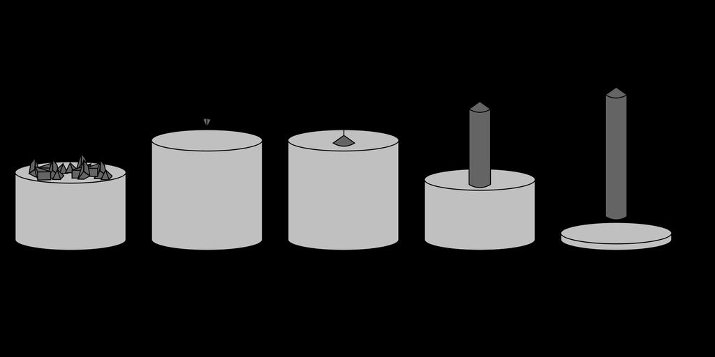
8 Czochralski Growth 8

9 Wafer Production 1.Ingot Growing 2.Shaping 3.Polishing 4.Cleansing Crystal Growth and Wafer Slicing Process Step 1: Obtaining the Sand Step 2: Preparing the Molten Silicon Bath Step 3: Making the Ingot Step 4: Preparing the Wafers Thickness Sorting Lapping & Etching Processes Thickness Sorting and Flatness Checking Polishing Process Final Dimensional and Electrical Properties Qualification Remove any cracked and damaged surface silicon on the surface 9
10 Types of Silicon Wafers Bulk polished Silicon Wafer Epi Silicon Wafer Heavily doped bulk wafers with moderately to lightly doped epitaxial silicon layer Immunity to latch-up Silicon on Insulator Wafer increase performance Eliminate latch-up silicon dioxide or sapphire 10
11 Epitaxial Growth the Greek roots epi (above) and taxis (in ordered manner)--> "to arrange upon". Epitax: the deposition of a crystalline overlayer on a crystalline substrate Epitaxial growth: there must be one or more preferred orientations of the overlayer with respect to the substrate the overlayer - an epitaxial film or epitaxial layer Epitaxial films may be grown from gaseous or liquid precursors. VPE (Vapor Phase Epitaxy) LPE (Liquid Phase Epitaxy) SPE (Solid Phase Epitaxy) If an epitaxial film is deposited on a substrate of the same composition, the process is called homoepitaxy; otherwise it is called heteroepitaxy. 11

12 Wafer Fabrication (1) Wafer production Wafer fabrication a procedure composed of many repeated sequential processes to produce complete electrical or photonic circuits. electrical circuit specifications circuit layout programs (computer aided design) photomask production 12
13 Wafer Fabrication (2) Photolithography Apply oxide Photoresist application (PR) Exposure and developing (Cr + glass) Etching Oxide Photoresist removal Silicon wafers start out blank and pure. The circuits are built in layers. photo-sensitive resistance patterns are photo-masked then exposed to short-wave ultraviolet light the unexposed areas are thus etched away and cleaned. Hot chemical vapors are deposited on to the desired zones and baked the vapors are permeated into the desired zones. In some cases, ions, such as O2+ or O+, are implanted These steps are often repeated many hundreds of times 13


14 Wafer Fabrication (3) Simplified illustration of the process of fabrication of a CMOS inverter Each etch step is detailed in the previous slide Oxidation Layering Photo lithography Etching Diffusion Thin Film Silicon wafers start out blank and pure. The circuits are built in layers. photo-sensitive resistance patterns are photo-masked then exposed to short-wave ultraviolet light the unexposed areas are thus etched away and cleaned. Hot chemical vapors are deposited on to the desired zones and baked the vapors are permeated into the desired zones. In some cases, ions, such as O2+ or O+, are implanted 14
15 Thermal Oxidation SiO2 : * Insulator * A good diffusion mask Very good etching selectivity Thermal oxidation is a way to produces a thin layer of oxide (usually silicon dioxide) on the surface of a wafer : High Temperature Oxide layer (HTO) forces an oxidizing agent to diffuse into the wafer at high temperature and react with it. may use either water vapor (wet oxidation) or molecular oxygen (dry oxidation) as the oxidant performed in furnaces, at temperatures between 800 and 1200 C. a single furnace accepts many wafers at the same time 15


16 Photolithography a process to pattern parts of a thin film or the bulk of a substrate uses light to transfer a geometric pattern from a photomask to a lightsensitive chemical "photoresist" on the substrate. either engraves the exposure pattern into, or enables deposition of a new material in the desired pattern upon, the material underneath the photo resist. 16
17 Etching used to chemically remove layers from the surface of a wafer part of the wafer is protected from the etchant by a "masking" material the masking material is a photoresist which has been patterned using photolithography. a more durable mask, such as silicon nitride Wet etching liquid-phase ("wet") etchants the wafer can be immersed in a bath of etchant buffered hydrofluoric acid (BHF) Anisotropic wet etching Orientation dependent etching Some wet etchants etch crystalline materials at very different rates depending upon which crystal face is exposed Plasma etching Modern VLSI processes avoid wet etching, and use plasma etching instead. Plasma etchers can operate in several modes by adjusting the parameters of the plasma. 17

18 Doping Extrinsic semiconductors with a larger electron concentration than hole concentration are known as n-type semiconductors. The phrase 'n-type' comes from the negative charge of the electron. In n-type semiconductors, electrons are the majority carriers and holes are the minority carriers. N-type semiconductors are created by doping an intrinsic semiconductor with donor impurities. As opposed to n-type semiconductors, p-type semiconductors have a larger hole concentration than electron concentration. The phrase 'p-type' refers to the positive charge of the hole. In p-type semiconductors, holes are the majority carriers and electrons are the minority carriers. P-type semiconductors are created by doping an intrinsic semiconductor with acceptor impurities. Diffusion : The spread of particles through random motion from regions of higher concentration to regions of lower concentration Ion implantation : Bombarding the substrate with ions accelerated to high velocities 18

.")
19 Diffusion A diffusion process in science. Some particles are dissolved in a glass of water. Initially, the particles are all near one corner of the glass. If the particles all randomly move around ("diffuse") in the water, then the particles will eventually become distributed randomly and uniformly, and organized (but diffusion will still continue to occur, just that there will be no net flux). Predeposition : to introduce the required dose of dopant into the substrate. Drive-In : a subsequent drive-in anneal then redistributes the dopant giving the required junction depth and surface concentration. 19


20 Ion Implantation Ion implantation is a materials engineering process by which ions of a material are accelerated in an electrical field and impacted into a solid. This process is used to change the physical, chemical, or electrical properties of the solid. 20
21 Thin Film Deposition thin: a layer of material ranging from fractions of a nanometer (monolayer) to several micrometers in thickness. the act of applying a thin film to a surface onto a substrate or onto previously deposited layers molecular beam epitaxy: a single layer of atoms Chemical deposition Physical deposition 21
22 Chemical Deposition a fluid precursor undergoes a chemical change at a solid surface, leaving a solid layer. like the formation of soot on a cool object when it is placed inside a flame. deposition happens on every surface, with little regard to direction; tend to be conformal, rather than directional. A conformal film defines a morphologically uneven interface with another body and has a thickness that is the same everywhere along the interface. Plating Chemical solution deposition (CSD) or Chemical bath deposition (CBD) Spin coating or spin casting Chemical vapor deposition (CVD) Plasma enhanced CVD (PECVD) Atomic layer deposition (ALD) 22
23 Physical Deposition mechanical, electromechanical or thermodynamic means like the formation of frost most engineering materials are held together by relatively high energies chemical reactions are not used to store these energies require a low-pressure vapor environment to function properly most can be classified as physical vapor deposition (PVD). Thermal evaporator Electron beam evaporator Molecular beam epitaxy (MBE) Sputtering Pulsed laser deposition Cathodic arc deposition (arc-pvd) Electrohydrodynamic deposition (Electrospray deposition) 23
24 Metallization coating metal on the surface of non-metallic objects. Plating relies on liquid precursors, often a solution of water with a salt of the metal to be deposited. Some plating processes are driven entirely by reagents in the solution (usually for noble metals), but by far the most commercially important process is electroplating. Chemical vapor deposition (CVD) generally uses a gas-phase precursor, often a halide or hydride of the element to be deposited. In the case of MOCVD, an organometallic gas is used. Commercial techniques often use very low pressures of precursor gas. Physical vapor deposition (PVD).The material to be deposited is placed in an energetic, entropic environment, so that particles of material escape its surface. Facing this source is a cooler surface which draws energy from these particles as they arrive, allowing them to form a solid layer. The whole system is kept in a vacuum deposition chamber, to allow the particles to travel as freely as possible. Since particles tend to follow a straight path, films deposited by physical means are commonly directional, rather than conformal. 24
25 Dielectric Insulator: SiO2 Si2N4 SiON Plasma enhanced CVD (PECVD) uses an ionized vapor, or plasma, as a precursor. Unlike the soot example above, commercial PECVD relies on electromagnetic means (electric current, microwave excitation), rather than a chemical reaction, to produce a plasma. Spin coating or spin casting, uses a liquid precursor, or sol-gel precursor deposited onto a smooth, flat substrate which is subsequently spun at a high velocity to centrifugally spread the solution over the substrate. The speed at which the solution is spun and the viscosity of the sol determine the ultimate thickness of the deposited film. Repeated depositions can be carried out to increase the thickness of films as desired. Thermal treatment is often carried out in order to crystallize the amorphous spin coated film (orientations). Atomic layer deposition (ALD) uses gaseous precursor to deposit conformal thin films one layer at a time. Two half reactions, run in sequence and repeated for each layer, in order to ensure total layer saturation. As a result of the stepwise, the process is slower than CVD, however it can be run at low temperatures, unlike CVD. 25
26 Mask 26
27 References [1]
Czochralski Crystal Growth
 Czochralski Crystal Growth Crystal Pulling Crystal Ingots Shaping and Polishing 300 mm wafer 1 2 Advantage of larger diameter wafers Wafer area larger Chip area larger 3 4 Large-Diameter Wafer Handling
Fabrication Technology
 Fabrication Technology By B.G.Balagangadhar Department of Electronics and Communication Ghousia College of Engineering, Ramanagaram 1 OUTLINE Introduction Why Silicon The purity of Silicon Czochralski
Chapter 3 CMOS processing technology
 Chapter 3 CMOS processing technology (How to make a CMOS?) Si + impurity acceptors(p-type) donors (n-type) p-type + n-type => pn junction (I-V) 3.1.1 (Wafer) Wafer = A disk of silicon (0.25 mm - 1 mm thick),
Microstructure of Electronic Materials. Amorphous materials. Single-Crystal Material. Professor N Cheung, U.C. Berkeley
 Microstructure of Electronic Materials Amorphous materials Single-Crystal Material 1 The Si Atom The Si Crystal diamond structure High-performance semiconductor devices require defect-free crystals 2 Crystallographic
Fabrication Process. Crystal Growth Doping Deposition Patterning Lithography Oxidation Ion Implementation CONCORDIA VLSI DESIGN LAB
 Fabrication Process Crystal Growth Doping Deposition Patterning Lithography Oxidation Ion Implementation 1 Fabrication- CMOS Process Starting Material Preparation 1. Produce Metallurgical Grade Silicon
CHAPTER - 4 CMOS PROCESSING TECHNOLOGY
 CHAPTER - 4 CMOS PROCESSING TECHNOLOGY Samir kamal Spring 2018 4.1 CHAPTER OBJECTIVES 1. Introduce the CMOS designer to the technology that is responsible for the semiconductor devices that might be designed
CS/ECE 5710/6710. N-type Transistor. N-type from the top. Diffusion Mask. Polysilicon Mask. CMOS Processing
 CS/ECE 5710/6710 CMOS Processing Addison-Wesley N-type Transistor D G +Vgs + Vds S N-type from the top i electrons - Diffusion Mask Mask for just the diffused regions Top view shows patterns that make
Metallization deposition and etching. Material mainly taken from Campbell, UCCS
 Metallization deposition and etching Material mainly taken from Campbell, UCCS Application Metallization is back-end processing Metals used are aluminum and copper Mainly involves deposition and etching,
Physics and Material Science of Semiconductor Nanostructures
 Physics and Material Science of Semiconductor Nanostructures PHYS 570P Prof. Oana Malis Email: omalis@purdue.edu Today Bulk semiconductor growth Single crystal techniques Nanostructure fabrication Epitaxial
ELEC 3908, Physical Electronics, Lecture 4. Basic Integrated Circuit Processing
 ELEC 3908, Physical Electronics, Lecture 4 Basic Integrated Circuit Processing Lecture Outline Details of the physical structure of devices will be very important in developing models for electrical behavior
Microelettronica. Planar Technology for Silicon Integrated Circuits Fabrication. 26/02/2017 A. Neviani - Microelettronica
 Microelettronica Planar Technology for Silicon Integrated Circuits Fabrication 26/02/2017 A. Neviani - Microelettronica Introduction Simplified crosssection of an nmosfet and a pmosfet Simplified crosssection
The Physical Structure (NMOS)
") The Physical Structure (NMOS) Al SiO2 Field Oxide Gate oxide S n+ Polysilicon Gate Al SiO2 SiO2 D n+ L channel P Substrate Field Oxide contact Metal (S) n+ (G) L W n+ (D) Poly 1 3D Perspective 2 3 Fabrication
The Physical Structure (NMOS) Al SiO2 Field Oxide Gate oxide S n+ Polysilicon Gate Al SiO2 SiO2 D n+ L channel P Substrate Field Oxide contact Metal (S) n+ (G) L W n+ (D) Poly 1 3D Perspective 2 3 Fabrication
A discussion of crystal growth, lithography, etching, doping, and device structures is presented in
 Chapter 5 PROCESSING OF DEVICES A discussion of crystal growth, lithography, etching, doping, and device structures is presented in the following overview gures. SEMICONDUCTOR DEVICE PROCESSING: AN OVERVIEW
Chapter 2 MOS Fabrication Technology
 Chapter 2 MOS Fabrication Technology Abstract This chapter is concerned with the fabrication of metal oxide semiconductor (MOS) technology. Various processes such as wafer fabrication, oxidation, mask
Semiconductor device fabrication
 REVIEW Semiconductor device fabrication is the process used to create the integrated circuits (silicon chips) that are present in everyday electrical and electronic devices. It is a multiplestep sequence
Lecture 22: Integrated circuit fabrication
 Lecture 22: Integrated circuit fabrication Contents 1 Introduction 1 2 Layering 4 3 Patterning 7 4 Doping 8 4.1 Thermal diffusion......................... 10 4.2 Ion implantation.........................
Chapter 3 Silicon Device Fabrication Technology
 Chapter 3 Silicon Device Fabrication Technology Over 10 15 transistors (or 100,000 for every person in the world) are manufactured every year. VLSI (Very Large Scale Integration) ULSI (Ultra Large Scale
ECE 440 Lecture 27 : Equilibrium P-N Junctions I Class Outline:
 ECE 440 Lecture 27 : Equilibrium P-N Junctions I Class Outline: Fabrication of p-n junctions Contact Potential Things you should know when you leave Key Questions What are the necessary steps to fabricate
EE 5344 Introduction to MEMS. CHAPTER 3 Conventional Si Processing
 3. Conventional licon Processing Micromachining, Microfabrication. EE 5344 Introduction to MEMS CHAPTER 3 Conventional Processing Why silicon? Abundant, cheap, easy to process. licon planar Integrated
PROCESS FLOW AN INSIGHT INTO CMOS FABRICATION PROCESS
 Contents: VI Sem ECE 06EC63: Analog and Mixed Mode VLSI Design PROCESS FLOW AN INSIGHT INTO CMOS FABRICATION PROCESS 1. Introduction 2. CMOS Fabrication 3. Simplified View of Fabrication Process 3.1 Alternative
Process Flow in Cross Sections
 Process Flow in Cross Sections Process (simplified) 0. Clean wafer in nasty acids (HF, HNO 3, H 2 SO 4,...) --> wear gloves! 1. Grow 500 nm of SiO 2 (by putting the wafer in a furnace with O 2 2. Coat
Figure 2.3 (cont., p. 60) (e) Block diagram of Pentium 4 processor with 42 million transistors (2000). [Courtesy Intel Corporation.
 (e) Block diagram of Pentium 4 processor with 42 million transistors (2000). [Courtesy Intel Corporation.") Figure 2.1 (p. 58) Basic fabrication steps in the silicon planar process: (a) oxide formation, (b) selective oxide removal, (c) deposition of dopant atoms on wafer, (d) diffusion of dopant atoms into exposed
Figure 2.1 (p. 58) Basic fabrication steps in the silicon planar process: (a) oxide formation, (b) selective oxide removal, (c) deposition of dopant atoms on wafer, (d) diffusion of dopant atoms into exposed
Lect. 2: Basics of Si Technology
 Unit processes Thin Film Deposition Etching Ion Implantation Photolithography Chemical Mechanical Polishing 1. Thin Film Deposition Layer of materials ranging from fractions of nanometer to several micro-meters
Microelectronics. Integrated circuits. Introduction to the IC technology M.Rencz 11 September, Expected decrease in line width
 Microelectronics Introduction to the IC technology M.Rencz 11 September, 2002 9/16/02 1/37 Integrated circuits Development is controlled by the roadmaps. Self-fulfilling predictions for the tendencies
EE40 Lec 22. IC Fabrication Technology. Prof. Nathan Cheung 11/19/2009
 Suggested Reading EE40 Lec 22 IC Fabrication Technology Prof. Nathan Cheung 11/19/2009 300mm Fab Tour http://www-03.ibm.com/technology/manufacturing/technology_tour_300mm_foundry.html Overview of IC Technology
VLSI Technology. By: Ajay Kumar Gautam
 By: Ajay Kumar Gautam Introduction to VLSI Technology, Crystal Growth, Oxidation, Epitaxial Process, Diffusion Process, Ion Implantation, Lithography, Etching, Metallization, VLSI Process Integration,
Fabrication and Layout
 ECEN454 Digital Integrated Circuit Design Fabrication and Layout ECEN 454 3.1 A Glimpse at MOS Device Polysilicon Aluminum ECEN 475 4.2 1 Material Classification Insulators Glass, diamond, silicon oxide
Silicon Manufacturing
 Silicon Manufacturing Group Members Young Soon Song Nghia Nguyen Kei Wong Eyad Fanous Hanna Kim Steven Hsu th Fundamental Processing Steps 1.Silicon Manufacturing a) Czochralski method. b) Wafer Manufacturing
IC/MEMS Fabrication - Outline. Fabrication
 IC/MEMS Fabrication - Outline Fabrication overview Materials Wafer fabrication The Cycle: Deposition Lithography Etching Fabrication IC Fabrication Deposition Spin Casting PVD physical vapor deposition
Introduction to CMOS VLSI Design. Layout, Fabrication, and Elementary Logic Design
 Introduction to CMOS VLSI Design Layout, Fabrication, and Elementary Logic Design CMOS Fabrication CMOS transistors are fabricated on silicon wafer Lithography process similar to printing press On each
Lecture 19 Microfabrication 4/1/03 Prof. Andy Neureuther
 EECS 40 Spring 2003 Lecture 19 Microfabrication 4/1/03 Prof. ndy Neureuther How are Integrated Circuits made? Silicon wafers Oxide formation by growth or deposition Other films Pattern transfer by lithography
VLSI INTRODUCTION P.VIDYA SAGAR ( ASSOCIATE PROFESSOR) Department of Electronics and Communication Engineering, VBIT
 Department of Electronics and Communication Engineering, VBIT") VLSI INTRODUCTION P.VIDYA SAGAR ( ASSOCIATE PROFESSOR) contents UNIT I INTRODUCTION: Introduction to IC Technology MOS, PMOS, NMOS, CMOS & BiCMOS technologies. BASIC ELECTRICAL PROPERTIES : Basic Electrical
VLSI INTRODUCTION P.VIDYA SAGAR ( ASSOCIATE PROFESSOR) contents UNIT I INTRODUCTION: Introduction to IC Technology MOS, PMOS, NMOS, CMOS & BiCMOS technologies. BASIC ELECTRICAL PROPERTIES : Basic Electrical
Molecular Beam Epitaxy (MBE) BY A.AKSHAYKRANTH JNTUH
 BY A.AKSHAYKRANTH JNTUH") Molecular Beam Epitaxy (MBE) BY A.AKSHAYKRANTH JNTUH CONTENTS Introduction What is Epitaxy? Epitaxy Techniques Working Principle of MBE MBE process & Epitaxial growth Working conditions Operation Control
Molecular Beam Epitaxy (MBE) BY A.AKSHAYKRANTH JNTUH CONTENTS Introduction What is Epitaxy? Epitaxy Techniques Working Principle of MBE MBE process & Epitaxial growth Working conditions Operation Control
Mostafa Soliman, Ph.D. May 5 th 2014
 Mostafa Soliman, Ph.D. May 5 th 2014 Mostafa Soliman, Ph.D. 1 Basic MEMS Processes Front-End Processes Back-End Processes 2 Mostafa Soliman, Ph.D. Wafers Deposition Lithography Etch Chips 1- Si Substrate
EECS130 Integrated Circuit Devices
 EECS130 Integrated Circuit Devices Professor Ali Javey 9/13/2007 Fabrication Technology Lecture 1 Silicon Device Fabrication Technology Over 10 15 transistors (or 100,000 for every person in the world)
Ajay Kumar Gautam [VLSI TECHNOLOGY] VLSI Technology for 3RD Year ECE/EEE Uttarakhand Technical University
![Ajay Kumar Gautam [VLSI TECHNOLOGY] VLSI Technology for 3RD Year ECE/EEE Uttarakhand Technical University](/thumbs/75/72824557.jpg "Ajay Kumar Gautam [VLSI TECHNOLOGY] VLSI Technology for 3RD Year ECE/EEE Uttarakhand Technical University") 2014 Ajay Kumar Gautam [VLSI TECHNOLOGY] VLSI Technology for 3RD Year ECE/EEE Uttarakhand Technical University Page1 Syllabus UNIT 1 Introduction to VLSI Technology: Classification of ICs, Scale of integration,
2014 Ajay Kumar Gautam [VLSI TECHNOLOGY] VLSI Technology for 3RD Year ECE/EEE Uttarakhand Technical University Page1 Syllabus UNIT 1 Introduction to VLSI Technology: Classification of ICs, Scale of integration,
Lecture 0: Introduction
 Lecture 0: Introduction Introduction Integrated circuits: many transistors on one chip. Very Large Scale Integration (VLSI): bucketloads! Complementary Metal Oxide Semiconductor Fast, cheap, low power
Microfabrication of Integrated Circuits
 Microfabrication of Integrated Circuits OUTLINE History Basic Processes Implant; Oxidation; Photolithography; Masks Layout and Process Flow Device Cross Section Evolution Lecture 38, 12/05/05 Reading This
Review of CMOS Processing Technology
 - Scaling and Integration Moore s Law Unit processes Thin Film Deposition Etching Ion Implantation Photolithography Chemical Mechanical Polishing 1. Thin Film Deposition Layer of materials ranging from
PROCESSING OF INTEGRATED CIRCUITS
 PROCESSING OF INTEGRATED CIRCUITS Overview of IC Processing (Part I) Silicon Processing Lithography Layer Processes Use in IC Fabrication (Part II) Integrating the Fabrication Steps IC Packaging (Part
Complexity of IC Metallization. Early 21 st Century IC Technology
 EECS 42 Introduction to Digital Electronics Lecture # 25 Microfabrication Handout of This Lecture. Today: how are Integrated Circuits made? Silicon wafers Oxide formation by growth or deposition Other
KGC SCIENTIFIC Making of a Chip
 KGC SCIENTIFIC www.kgcscientific.com Making of a Chip FROM THE SAND TO THE PACKAGE, A DIAGRAM TO UNDERSTAND HOW CPU IS MADE? Sand CPU CHAIN ANALYSIS OF SEMICONDUCTOR Material for manufacturing process
CMOS VLSI Design. Introduction. All materials are from the textbook Weste and Harris, 3 rd Edition CMOS VLSI DESIGN. Introduction
 CMOS VLSI Design Introduction ll materials are from the textbook Weste and Harris, 3 rd Edition CMOS VLSI DESIGN Introduction Chapter previews the entire field, subsequent chapters elaborate on specific
Doping and Oxidation
 Technische Universität Graz Institute of Solid State Physics Doping and Oxidation Franssila: Chapters 13,14, 15 Peter Hadley Technische Universität Graz Institute of Solid State Physics Doping Add donors
VLSI Digital Systems Design
 VLSI Digital Systems Design CMOS Processing cmpe222_03process_ppt.ppt 1 Si Purification Chemical purification of Si Zone refined Induction furnace Si ingot melted in localized zone Molten zone moved from
EE 330 Lecture 9. IC Fabrication Technology Part 2
 EE 330 Lecture 9 IC Fabrication Technology Part 2 Quiz 8 A 2m silicon crystal is cut into wafers using a wire saw. If the wire diameter is 220um and the wafer thickness is 350um, how many wafers will this
Making of a Chip Illustrations
 Making of a Chip Illustrations 22nm 3D/Trigate Transistors Version April 2015 1 The illustrations on the following foils are low resolution images that visually support the explanations of the individual
EE 330 Lecture 9. IC Fabrication Technology Part II. -Oxidation -Epitaxy -Polysilicon -Planarization -Resistance and Capacitance in Interconnects
 EE 330 Lecture 9 IC Fabrication Technology Part II -Oxidation -Epitaxy -Polysilicon -Planarization -Resistance and Capacitance in Interconnects Review from Last Time Etching Dry etch (anisotropic) SiO
Crystal Growth and Wafer Fabrication. K.Sivasankaran, Assistant Professor (Senior), VLSI Division, School of Electronics Engineering, VIT
, VLSI Division, School of Electronics Engineering, VIT") Crystal Growth and Wafer Fabrication K.Sivasankaran, Assistant Professor (Senior), VLSI Division, School of Electronics Engineering, VIT Crystal growth Obtaining sand Raw Polysilicon Czochralski Process
Crystal Growth and Wafer Fabrication K.Sivasankaran, Assistant Professor (Senior), VLSI Division, School of Electronics Engineering, VIT Crystal growth Obtaining sand Raw Polysilicon Czochralski Process
Low Power VLSI Circuits and Systems Prof. Ajit Pal Department of Computer Science and Engineering Indian Institute of Technology, Kharagpur
 Low Power VLSI Circuits and Systems Prof. Ajit Pal Department of Computer Science and Engineering Indian Institute of Technology, Kharagpur Lecture No. # 02 MOS Transistors - I Hello and welcome to today
Semiconductor Device Fabrication
 5 May 2003 Review Homework 6 Semiconductor Device Fabrication William Shockley, 1945 The network before the internet Bell Labs established a group to develop a semiconductor replacement for the vacuum
FABRICATION ENGINEERING MICRO- NANOSCALE ATTHE AND. Fourth Edition STEPHEN A. CAMPBELL. of Minnesota. University OXFORD UNIVERSITY PRESS
 AND FABRICATION ENGINEERING ATTHE MICRO- NANOSCALE Fourth Edition STEPHEN A. CAMPBELL University of Minnesota New York Oxford OXFORD UNIVERSITY PRESS CONTENTS Preface xiii prrt i OVERVIEW AND MATERIALS
CMOS Fabrication. Dr. Bassam Jamil. Adopted from slides of the textbook
 CMOS Fabrication Dr. Bassam Jamil Adopted from slides of the textbook CMOS Fabrication CMOS transistors are fabricated on silicon wafer Lithography process similar to printing press On each step, different
PY2N20 Material Properties and Phase Diagrams
 PY2N20 Material Properties and Phase Diagrams Lecture 9 P. Stamenov, PhD School of Physics, TCD PY2N20-9 Semiconductor Wafer Production - Si Czochralski Growth Growth from melt Melt 99.999999% pure polycrystalline
Lecture #18 Fabrication OUTLINE
 Transistors on a Chip Lecture #18 Fabrication OUTLINE IC Fabrication Technology Introduction the task at hand Doping Oxidation Thin-film deposition Lithography Etch Lithography trends Plasma processing
Silicon Epitaxial CVD Want to create very sharp PN boundary grow one type layer on other in single crystal form High dopant layers on low dopant
 Silicon Epitaxial CVD Want to create very sharp PN boundary grow one type layer on other in single crystal form High dopant layers on low dopant substrate Creates latch up protection for CMOS Buried Epi
VLSI Design and Simulation
 VLSI Design and Simulation CMOS Processing Technology Topics CMOS Processing Technology Semiconductor Processing How do we make a transistor? Fabrication Process Wafer Processing Silicon single crystal
VLSI. Lecture 1. Jaeyong Chung System-on-Chips (SoC) Laboratory Incheon National University. Based on slides of David Money Harris
 Laboratory Incheon National University. Based on slides of David Money Harris") VLSI Lecture 1 Jaeyong Chung System-on-Chips (SoC) Laboratory Incheon National University Based on slides of David Money Harris Goals of This Course Learn the principles of VLSI design Learn to design
VLSI Lecture 1 Jaeyong Chung System-on-Chips (SoC) Laboratory Incheon National University Based on slides of David Money Harris Goals of This Course Learn the principles of VLSI design Learn to design
EE 5611 Introduction to Microelectronic Technologies Fall Tuesday, September 04, 2012 Lecture 01
 EE 5611 Introduction to Microelectronic Technologies Fall 2012 Tuesday, September 04, 2012 Lecture 01 1 Instructor: Jing Bai Contact Email: jingbai@d.umn.edu, hone: (218)726-8606, Office: MWAH 255 Webpage:
Most semiconductor devices contain at least one junction between p-type and n-type material. These p-n junctions are fundamental to the performance
 Ch. 5: p-n Junction Most semiconductor devices contain at least one junction between p-type and n-type material. These p-n junctions are fundamental to the performance of functions such as rectification,
ET3034TUx High efficiency concepts of c- Si wafer based solar cells
 ET3034TUx - 4.4 - High efficiency concepts of c- Si wafer based solar cells In the previous block we have discussed various technological aspects on crystalline silicon wafer based PV technology. In this
Atomic Layer Deposition(ALD)
") Atomic Layer Deposition(ALD) AlO x for diffusion barriers OLED displays http://en.wikipedia.org/wiki/atomic_layer_deposition#/media/file:ald_schematics.jpg Lam s market-leading ALTUS systems combine CVD
Atomic Layer Deposition(ALD) AlO x for diffusion barriers OLED displays http://en.wikipedia.org/wiki/atomic_layer_deposition#/media/file:ald_schematics.jpg Lam s market-leading ALTUS systems combine CVD
Chapter 2 Manufacturing Process
 Digital Integrated Circuits A Design Perspective Chapter 2 Manufacturing Process 1 CMOS Process 2 CMOS Process (n-well) Both NMOS and PMOS must be built in the same silicon material. PMOS in n-well NMOS
Microelectronic Device Instructional Laboratory. Table of Contents
 Introduction Process Overview Microelectronic Device Instructional Laboratory Introduction Description Flowchart MOSFET Development Process Description Process Steps Cleaning Solvent Cleaning Photo Lithography
1 MARCH 2017 FILM DEPOSITION NANOTECHNOLOGY
 1 MARCH 2017 FILM DEPOSITION NANOTECHNOLOGY PRESENTATION Pedro C. Feijoo E-mail: PedroCarlos.Feijoo@uab.cat FABRICATION TECHNOLOGIES FOR NANOELECTRONIC DEVICES. PEDRO C. FEIJOO 2 FILM GROWTH Chemical vapor
Silicon Epitaxial CVD Want to create very sharp PN boundary grow one type layer on other in single crystal form High dopant layers on low dopant
 Silicon Epitaxial CVD Want to create very sharp PN boundary grow one type layer on other in single crystal form High dopant layers on low dopant substrate Creates latch up protection for CMOS Buried Epi
Instructor: Dr. M. Razaghi. Silicon Oxidation
 SILICON OXIDATION Silicon Oxidation Many different kinds of thin films are used to fabricate discrete devices and integrated circuits. Including: Thermal oxides Dielectric layers Polycrystalline silicon
UT Austin, ECE Department VLSI Design 2. CMOS Fabrication, Layout Rules
 2. CMOS Fabrication, Layout, Design Rules Last module: Introduction to the course How a transistor works CMOS transistors This module: CMOS Fabrication Design Rules CMOS Fabrication CMOS transistors are
EE 5611 Introduction to Microelectronic Technologies Fall Tuesday, September 02, 2014 Lecture 01
 EE 5611 Introduction to Microelectronic Technologies Fall 2014 Tuesday, September 02, 2014 Lecture 01 1 Instructor: Jing Bai Contact Email: jingbai@d.umn.edu, hone: (218)726-8606, Office: MWAH 255 Webpage:
PHYS 534 (Fall 2008) Process Integration OUTLINE. Examples of PROCESS FLOW SEQUENCES. >Surface-Micromachined Beam
 Process Integration OUTLINE. Examples of PROCESS FLOW SEQUENCES. >Surface-Micromachined Beam") PHYS 534 (Fall 2008) Process Integration Srikar Vengallatore, McGill University 1 OUTLINE Examples of PROCESS FLOW SEQUENCES >Semiconductor diode >Surface-Micromachined Beam Critical Issues in Process
PHYS 534 (Fall 2008) Process Integration Srikar Vengallatore, McGill University 1 OUTLINE Examples of PROCESS FLOW SEQUENCES >Semiconductor diode >Surface-Micromachined Beam Critical Issues in Process
TOWARD MEMS!Instructor: Riadh W. Y. Habash
 TOWARD MEMS!Instructor: Riadh W. Y. Habash Students are presented with aspects of general production and manufacturing of integrated circuit (IC) products to enable them to better liaise with and participate
Today s Class. Materials for MEMS
 Lecture 2: VLSI-based Fabrication for MEMS: Fundamentals Prasanna S. Gandhi Assistant Professor, Department of Mechanical Engineering, Indian Institute of Technology, Bombay, Recap: Last Class What is
EE 434 Lecture 9. IC Fabrication Technology
 EE 434 Lecture 9 IC Fabrication Technology Quiz 7 The layout of a film resistor with electrodes A and B is shown. If the sheet resistance of the film is 40 /, determine the resistance between nodes A and
Physical Vapor Deposition (PVD) Zheng Yang
 Zheng Yang") Physical Vapor Deposition (PVD) Zheng Yang ERF 3017, email: yangzhen@uic.edu Page 1 Major Fabrication Steps in MOS Process Flow UV light Mask oxygen Silicon dioxide photoresist exposed photoresist oxide
Physical Vapor Deposition (PVD) Zheng Yang ERF 3017, email: yangzhen@uic.edu Page 1 Major Fabrication Steps in MOS Process Flow UV light Mask oxygen Silicon dioxide photoresist exposed photoresist oxide
LANDOLT-BÖRNSTEIN. Zahlenwerte und Funktionen aus Naturwissenschaften und Technik. Neue Serie. Gesamtherausgabe: K.-H. Hellwege O.
 LANDOLT-BÖRNSTEIN Zahlenwerte und Funktionen aus Naturwissenschaften und Technik Neue Serie Gesamtherausgabe: K.-H. Hellwege O. Madelung Gruppe III: Kristall- und Festkörperphysik Band 17 Halbleiter Herausgeber:
Department of Electrical Engineering. Jungli, Taiwan
 Chapter 3 Fabrication of CMOS Integrated Circuits Jin-Fu Li Department of Electrical Engineering National Central University Jungli, Taiwan Background Outline The CMOS Process Flow Design Rules Latchup
INTEGRATED-CIRCUIT TECHNOLOGY
 INTEGRATED-CIRCUIT TECHNOLOGY 0. Silicon crystal growth and wafer preparation 1. Processing Steps 1.1. Photolitography 1.2. Oxidation 1.3. Layer Deposition 1.4. Etching 1.5. Diffusion 1.6 Backend: assembly,
PHYSICAL ELECTRONICS(ECE3540) Brook Abegaz, Tennessee Technological University, Fall 2013
 Brook Abegaz, Tennessee Technological University, Fall 2013") PHYSICAL ELECTRONICS(ECE3540) Brook Abegaz, Tennessee Technological University, Fall 2013 1 Chapter 1 The Crystal Structure of Solids Physical Electronics: Includes aspects of the physics of electron movement
PHYSICAL ELECTRONICS(ECE3540) Brook Abegaz, Tennessee Technological University, Fall 2013 1 Chapter 1 The Crystal Structure of Solids Physical Electronics: Includes aspects of the physics of electron movement
EE 330 Lecture 9. IC Fabrication Technology Part II. -Oxidation -Epitaxy -Polysilicon -Planarization -Resistance and Capacitance in Interconnects
 EE 330 Lecture 9 IC Fabrication Technology Part II -Oxidation -Epitaxy -Polysilicon -Planarization -Resistance and Capacitance in Interconnects Review from Last Time IC Fabrication Technology Crystal Preparation
FABRICATION OF CMOS INTEGRATED CIRCUITS. Dr. Mohammed M. Farag
 FABRICATION OF CMOS INTEGRATED CIRCUITS Dr. Mohammed M. Farag Outline Overview of CMOS Fabrication Processes The CMOS Fabrication Process Flow Design Rules EE 432 VLSI Modeling and Design 2 CMOS Fabrication
Lecture Day 2 Deposition
 Deposition Lecture Day 2 Deposition PVD - Physical Vapor Deposition E-beam Evaporation Thermal Evaporation (wire feed vs boat) Sputtering CVD - Chemical Vapor Deposition PECVD LPCVD MVD ALD MBE Plating
Thermal Evaporation. Theory
 Thermal Evaporation Theory 1. Introduction Procedures for depositing films are a very important set of processes since all of the layers above the surface of the wafer must be deposited. We can classify
Lecture 1A: Manufacturing& Layout
 Introduction to CMOS VLSI Design Lecture 1A: Manufacturing& Layout David Harris Harvey Mudd College Spring 2004 Steven Levitan Fall 2008 1 The Manufacturing Process For a great tour through the IC manufacturing
Bulk crystal growth. A reduction in Lg will increase g m and f oper but with some costs
 Bulk crystal growth The progress of solid state device technology has depended not only on the development of device concepts but also on the improvement of materials. A reduction in Lg will increase g
Surface micromachining and Process flow part 1
 Surface micromachining and Process flow part 1 Identify the basic steps of a generic surface micromachining process Identify the critical requirements needed to create a MEMS using surface micromachining
EE6303 LINEAR INTEGRATED CIRCUITS AND APPLICATIONS 2 MARK QUESTIONS WITH ANSWERS UNIT I IC FABRICATION
 SRI VENKATESWARA COLLEGE OF ENGINEERING AND TECHNOLOGY TIRUPACHUR DEPARTMENT OFELECTRICAL AND ELECTRONICS ENGINEERING EE6303 LINEAR INTEGRATED CIRCUITS AND APPLICATIONS 1. Define an Integrated circuit.
Chapter 2 Problems. The CMOS technology we need to realize is shown below, from Figure 1-34 in the text. S P + N P + N WELL P +
 Chapter 2 roblems 2.1 Sketch a process flow that would result in the structure shown in Figure 1-34 by drawing a series of drawings similar to those in this chapter. You only need to describe the flow
CMOS Manufacturing process. Design rule set
 CMOS Manufacturing process Circuit design Set of optical masks Fabrication process Circuit designer Design rule set Process engineer All material: Chap. 2 of J. Rabaey, A. Chandrakasan, B. Nikolic, Digital
Temperature Scales. Questions. Temperature Conversions 7/21/2010. EE580 Solar Cells Todd J. Kaiser. Thermally Activated Processes
 7/1/010 EE80 Solar Cells Todd J. Kaiser Flow of Wafer in Fabrication Lecture 0 Microfabrication A combination of Applied Chemistry, Physics and ptics Thermal Processes Diffusion & xidation Photolithograpy
CSCI 4974 / 6974 Hardware Reverse Engineering. Lecture 5: Fabrication processes
 CSCI 4974 / 6974 Hardware Reverse Engineering Lecture 5: Fabrication processes QUIZ 3: CMOS layout Quiz Discussion Rationale If you know how something is put together, you can figure out how to take it
Semiconductor Manufacturing Technology. IC Fabrication Process Overview
 Semiconductor Manufacturing Technology Michael Quirk & Julian Serda October 00 by Prentice Hall Chapter 9 IC Fabrication Process Overview /4 Objectives After studying the material in this chapter, you
A Novel Low Temperature Self-Aligned Field Induced Drain Polycrystalline Silicon Thin Film Transistor by Using Selective Side-Etching Process
 Chapter 3 A Novel Low Temperature Self-Aligned Field Induced Drain Polycrystalline Silicon Thin Film Transistor by Using Selective Side-Etching Process 3.1 Introduction Low-temperature poly-si (LTPS) TFTs
Institute of Solid State Physics. Technische Universität Graz. Deposition. Franssila: Chapters 5 & 6. Peter Hadley
 Technische Universität Graz Institute of Solid State Physics Deposition Franssila: Chapters 5 & 6 Peter Hadley Silicon wafers Total Thickness Variation: a good 8" Prime wafer would be < 15 m Site flatness
EE 330 Lecture 8. IC Fabrication Technology Part II. - Oxidation - Epitaxy - Polysilicon - Interconnects
 EE 330 Lecture 8 IC Fabrication Technology Part II - Oxidation - Epitaxy - Polysilicon - Interconnects Review from Last Time MOS Transistor Bulk Source Gate Drain p-channel MOSFET Lightly-doped n-type
Chapter 2 OVERVIEW OF MEMS
 6 Chapter 2 OVERVIEW OF MEMS 2.1 MEMS and Microsystems The term MEMS is an abbreviation of microelectromechanical system. MEMS contains components ofsizes in 1 micrometer to 1 millimeter. The core element
Silver Diffusion Bonding and Layer Transfer of Lithium Niobate to Silicon
 Chapter 5 Silver Diffusion Bonding and Layer Transfer of Lithium Niobate to Silicon 5.1 Introduction In this chapter, we discuss a method of metallic bonding between two deposited silver layers. A diffusion
Schematic creation of MOS field effect transistor.
 Schematic creation of MOS field effect transistor. Gate electrode Drain electrode Source electrode Gate oxide Gate length Page 1 Step 0 The positively doped silicon wafer is first coated with an insulating