Microstructure of Electronic Materials. Amorphous materials. Single-Crystal Material. Professor N Cheung, U.C. Berkeley
|
|
|
- Cornelius Logan
- 5 years ago
- Views:
Transcription
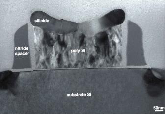
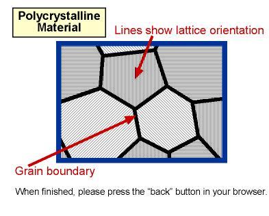
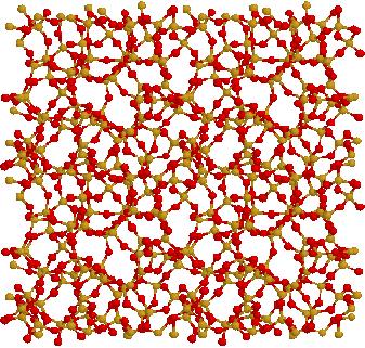
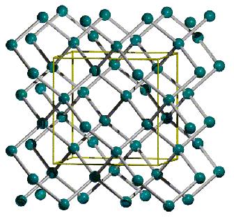
1 Microstructure of Electronic Materials Amorphous materials Single-Crystal Material 1


2 The Si Atom The Si Crystal diamond structure High-performance semiconductor devices require defect-free crystals 2


3 Crystallographic Planes Unit cell: Si lattice constant = 5.431Å 5 x 10²² atoms/cm3 View in <100> direction View in <110> direction View in <111> direction 3
4 Crystallographic Notation Miller Indices Notation (hkl) Interpretation {hkl} equivalent planes [hkl] crystal direction <hkl> equivalent directions crystal plane h: inverse x-intercept k: inverse y-intercept l: inverse z-intercept (Intercept values are in multiples of the lattice constant; h, k and l are reduced to 3 integers having the same ratio.) 4
5 Carrier Concentrations of Intrinsic (undoped) Si electron - Bottom of conduction band Energy gap =1.12 ev hole + Top of valence band n (electron conc) = p (hole conc) = ni 5


6 Dopants in Si By substituting a Si atom with a special impurity atom (Column V or Column III element), a conduction electron or hole is created. Donors: P, As, Sb Acceptors: B, Al, Ga, In 6


7 n-type Semiconductor If ND >> NA (such that ND NA 10 ni): = + ND /cm3 n-type NA /cm3 2 n ND N A and ni p ND N A Note n >> p 7
8 p-type Semiconductor If NA >> ND (such that NA ND 10 ni): = + ND /cm3 NA /cm3 p-type 2 p N A ND and ni n N A ND Note p >> n 8

9 Adding parts/billion to parts/thousand of dopants to pure Si can change resistivity by 8 orders of magnitude! 1 Note: -m = 100 Resistivity Range of Materials Si with dopants SiO2, Si3N4 -cm 9

10 Principle of Monolithic Process Integration * A sequence of Additive and Subtractive steps with lateral patterning Example: CMOS Integrated Circuit Processing Steps Si wafer
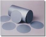
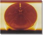
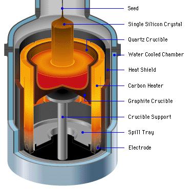
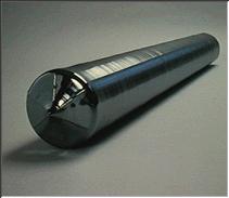
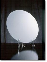
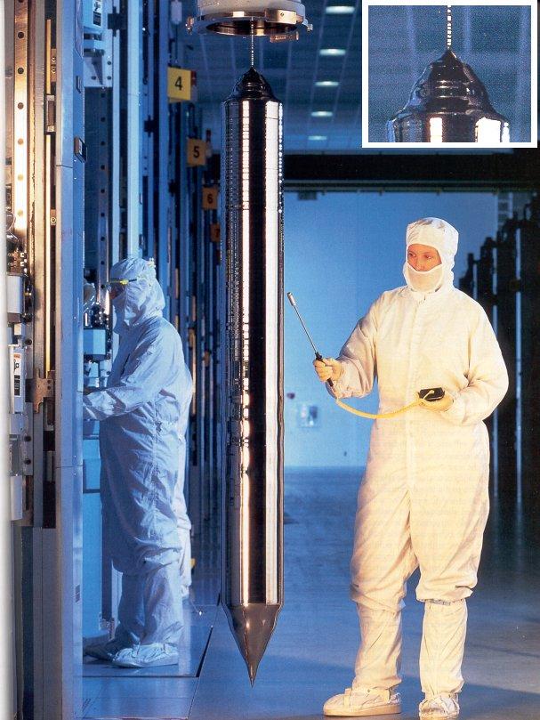
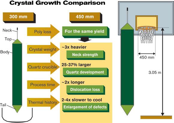
11 Czochralski Crystal Growth Crystal Pulling Shaping and Polishing Crystal Ingots 300 mm wafer 11
12 12
13 13

14 Purity of Starting IC Si Wafer % (so(so-called eleven nines )!! Maximum impurity of starting Si wafer is equivalent to 1 mg of sugar dissolved in an Olympic-size swimming pool..
*: Si 99.99 99.999%, US$ 30 40/kg Electronic Grade Silicon (EG): Si > 99.")
15 Solar Cell Grade Silicon For reference only Metallurgic Grade Silicon (MG): Si 90-99%, US$ 1 2.5/kg Solar Grade Silicon (SG)*: Si %, US$ 30 40/kg Electronic Grade Silicon (EG): Si > %, over US$ 60/kg

16 Photolithography glass plate chromium Processing Temperature Ambient Positive Resist Region exposed to light will be dissolved in development solution. 16
 Prebake, (4) Expose, (5) Post Exposure bake, (6) Develop, (7) Hard")
17 Example : Deep UV Photolithography Sequence: (1)Surface Prime, (2) Coat, (3) Prebake, (4) Expose, (5) Post Exposure bake, (6) Develop, (7) Hard Bake

18 Example : Deep UV Photolithography (continued)
")

19 Example : Deep UV Photolithography (continued) *All baking sub-steps are similar but with different temperature and time
 Ambient Isotropic (e.g. Wet Etching) 20")
20 Etching Pattern resist mask Etching thin film Etching completed Remove resist mask Anisotropic Processing Temperature (e.g. Reactive Ion Etching RIE ) Ambient Isotropic (e.g. Wet Etching) 20
21 Etching Selectivity Example: HF solution etches SiO2 but not Si HF SiO2 Si solution Si * A high etching selectivity is usually desired 21
 Si substrate Etching stops Etching continues Effect of different mask")
22 Anisotropic Wet Etching of Si Crystals Etchants : KOH or EDP (Ethylene-Diamine_Pyrocatechol) Cross-section Top view (100) Si substrate Etching stops Etching continues Effect of different mask opening 22
 - use O2. Dry oxidation Thick oxide growth (e.g. field oxide) - use H2O.")
23 Thermal Oxidation Processing Temperature oc Si + O2 SiO2 Si + 2 H2O SiO2 + 2H2 Oxide (Xox) thickness t t O2 (or H2O) diffuses through SiO2 and reacts with Si at the interface to form more SiO2. 1 m of SiO2 formed consumes 0.44 m of Si substrate. Thin oxide growth (e.g. gate oxide) - use O2. Dry oxidation Thick oxide growth (e.g. field oxide) - use H2O. Wet oxidation Oxidation time(t) 23
24 Uneven surface topography with window oxidation 1st oxidation SiO2 Si Si Realistic topography with 2-dimensional effect SiO2 Si Pattern oxide window by litho and etch 2nd oxidation SiO2 SiO2 Si Si Note uneven Si surface after window oxidation 24
25 Local Oxidation silicon nitride as oxidation mask O2 Si3N4 pad oxide ~100 A Si Thermal Oxidization LOCOS Process nitride SiO2 Si 25

26 Ion Implantation typically used to introduce dopants into semiconductors Ion Energy ~1 kev to 200 kev Processing Temperature Room temp during implantation. After implantation, a 900oC-1000oC anneal step is needed to: 1) activate dopants 2) restore Si crystallinity 26
![Diffusion To introduce dopants into semiconductors [ Predeposition] To spread out the dopant profile [](/docs-images/83/88047590/images/27-0.jpg "Drive-in] Processing Temperature 850-1150 oc D D0 e Q kt D Diffusion Constant Q Activation Energy T Temp in K")
27 Diffusion To introduce dopants into semiconductors [ Predeposition] To spread out the dopant profile [ Drive-in] Processing Temperature oc D D0 e Q kt D Diffusion Constant Q Activation Energy T Temp in K D as T 27
28 Predeposition Si surface concentration maintained at constant Cs (solid-solubility) during predep. Dose of dopant incorporation (in #/cm2) C s 2 Dt = 28
29 Predeposition and Drive-in Drive-in means removing dopant supply after Predep step and anneal at high temperature Half-gaussian depth profile after long drive-in. Predep only Predep +Drive-in Dopant dose conserved during drive-in. Diffusion distance Dt Concentration (in #/cm3) versus Depth 29
30 Physical Vapor Deposition (1) Evaporation Deposition Si Substrate Substrate at ~ room temp Deposited Al film (polycrystalline) evaporation Al charge (Tsource >>Tboiling of Al, 700OC) 30
31 Physical Vapor Deposition (2) Sputtering Deposition Si Substrate Substrate at room temp Deposited Al film (polycrystalline) Ar+ Ar ions with ~ kev kinetic energy Al atoms ejected due to Ar ion bombardment Al target 31
32 Chemical Vapor Deposition (CVD) 32
33 Chemical Vapor Deposition (CVD) of SiO2 Si (C 2 H 5 O ) 4 2 H 2 O SiO 2 4C 2 H 6 O or SiH 4 O 2 SiO 2 2H 2 LTO TEOS Temperature range: 350oC to 450oC for silane ~700oC for TEOS Process: Precursor gases dissociate at the wafer surface to form SiO2 No Si on the wafer surface is consumed Film thickness is controlled by the deposition time oxide thickness t time, t
34 Plasma Enhanced CVD Plasma generates dissocated and Ionized chemical species Lower CVD process temperature can be used. 34
35 Epitaxial Growth Processing Temperature oC Requires an ultra-clean Si surface prior to epi growth. Requires deposition of Si at very high temperature for perfect crystallinity. 35
36 Chemical Mechanical Polishing (CMP) Wafer is polished using a slurry containing silica abrasives (10-90 nm particle size) etching agents (e.g. dilute HF) Backing film provides elasticity between carrier and wafer Polishing pad made of polyurethane, with 1 m perforations rough surface to hold slurry Ambient Temperature 36
 layers shallow trench isolation (STI) copper metallization Shallow Trench Oxide p+ n p+ SiO2 p n+ p n+ ILD with 5 layers of Al")
37 Chemical Mechanical Polishing (CMP) CMP is used to planarize the surface of a wafer at various steps in the process of fabricating an integrated circuit. interlevel dielectric (ILD) layers shallow trench isolation (STI) copper metallization Shallow Trench Oxide p+ n p+ SiO2 p n+ p n+ ILD with 5 layers of Al wiring

 (2) (3) courtesy")

38 Copper Plating Dual Damascene Process (IBM Corporation) (1) (2) (3) courtesy of Sung Gyu Pyo, Hynix Semiconductor (4) (5)

39 Rapid Thermal Annealing (RTA) Special annealing tools have been developed to enable much faster temperature ramping, and precise control of annealing time ramp rates as fast as 200oC/second anneal times as short as 0.5 second typically single-wafer process chamber Sub-micron MOSFETs need ultra-shallow junctions (xj<50 nm) Dopant diffusion during activation anneal must be minimized Short annealing time (<1 min.) at high temperature is required Ordinary furnaces (e.g. used for thermal oxidation and CVD) heat and cool wafers at a slow rate (<50oC per minute)

40 Rapid Thermal Annealing Tools There are 2 types of RTA systems: 1. Furnace-based steady heat source + fast mechanical wafer transport 2. Lamp-based stationary wafer + time-varying optical output from lamp(s) Furnace RTA Lamp RTA A.T. Fiory, Proc. RTP2000
41 Microfabrication Module Summary List Lithography Thermal Oxidation Etching (Chemical, RIE) Ion Implantation Diffusion (Furnace Annealing, Rapid Thermal Annealing RTA) Physical Vapor Deposition PVD Chemical Vapor Deposition CVD, Epitaxial Growth, PECVD Chemical Mechanical Polishing CMP Metal Plating Others. 41
42 Pr o c e s s Te m p e r a t u r e in C PROCESSING TEMP RANGE AND MATERIAL FAILURE TEMP Si Melting Point (1450C) Al-Si Eutectic (560C) Photoresist Reflow (180C)
Czochralski Crystal Growth
 Czochralski Crystal Growth Crystal Pulling Crystal Ingots Shaping and Polishing 300 mm wafer 1 2 Advantage of larger diameter wafers Wafer area larger Chip area larger 3 4 Large-Diameter Wafer Handling
EE40 Lec 22. IC Fabrication Technology. Prof. Nathan Cheung 11/19/2009
 Suggested Reading EE40 Lec 22 IC Fabrication Technology Prof. Nathan Cheung 11/19/2009 300mm Fab Tour http://www-03.ibm.com/technology/manufacturing/technology_tour_300mm_foundry.html Overview of IC Technology
Microelettronica. Planar Technology for Silicon Integrated Circuits Fabrication. 26/02/2017 A. Neviani - Microelettronica
 Microelettronica Planar Technology for Silicon Integrated Circuits Fabrication 26/02/2017 A. Neviani - Microelettronica Introduction Simplified crosssection of an nmosfet and a pmosfet Simplified crosssection
Lecture #18 Fabrication OUTLINE
 Transistors on a Chip Lecture #18 Fabrication OUTLINE IC Fabrication Technology Introduction the task at hand Doping Oxidation Thin-film deposition Lithography Etch Lithography trends Plasma processing
Chapter 3 Silicon Device Fabrication Technology
 Chapter 3 Silicon Device Fabrication Technology Over 10 15 transistors (or 100,000 for every person in the world) are manufactured every year. VLSI (Very Large Scale Integration) ULSI (Ultra Large Scale
ELEC 3908, Physical Electronics, Lecture 4. Basic Integrated Circuit Processing
 ELEC 3908, Physical Electronics, Lecture 4 Basic Integrated Circuit Processing Lecture Outline Details of the physical structure of devices will be very important in developing models for electrical behavior
Fabrication Process. Crystal Growth Doping Deposition Patterning Lithography Oxidation Ion Implementation CONCORDIA VLSI DESIGN LAB
 Fabrication Process Crystal Growth Doping Deposition Patterning Lithography Oxidation Ion Implementation 1 Fabrication- CMOS Process Starting Material Preparation 1. Produce Metallurgical Grade Silicon
HOMEWORK 4 and 5. March 15, Homework is due on Monday March 30, 2009 in Class. Answer the following questions from the Course Textbook:
 HOMEWORK 4 and 5 March 15, 2009 Homework is due on Monday March 30, 2009 in Class. Chapter 7 Answer the following questions from the Course Textbook: 7.2, 7.3, 7.4, 7.5, 7.6*, 7.7, 7.9*, 7.10*, 7.16, 7.17*,
Doping and Oxidation
 Technische Universität Graz Institute of Solid State Physics Doping and Oxidation Franssila: Chapters 13,14, 15 Peter Hadley Technische Universität Graz Institute of Solid State Physics Doping Add donors
INTEGRATED-CIRCUIT TECHNOLOGY
 INTEGRATED-CIRCUIT TECHNOLOGY 0. Silicon crystal growth and wafer preparation 1. Processing Steps 1.1. Photolitography 1.2. Oxidation 1.3. Layer Deposition 1.4. Etching 1.5. Diffusion 1.6 Backend: assembly,
Chapter 3 CMOS processing technology
 Chapter 3 CMOS processing technology (How to make a CMOS?) Si + impurity acceptors(p-type) donors (n-type) p-type + n-type => pn junction (I-V) 3.1.1 (Wafer) Wafer = A disk of silicon (0.25 mm - 1 mm thick),
EE 5344 Introduction to MEMS. CHAPTER 3 Conventional Si Processing
 3. Conventional licon Processing Micromachining, Microfabrication. EE 5344 Introduction to MEMS CHAPTER 3 Conventional Processing Why silicon? Abundant, cheap, easy to process. licon planar Integrated
EECS130 Integrated Circuit Devices
 EECS130 Integrated Circuit Devices Professor Ali Javey 9/13/2007 Fabrication Technology Lecture 1 Silicon Device Fabrication Technology Over 10 15 transistors (or 100,000 for every person in the world)
The Physical Structure (NMOS)
") The Physical Structure (NMOS) Al SiO2 Field Oxide Gate oxide S n+ Polysilicon Gate Al SiO2 SiO2 D n+ L channel P Substrate Field Oxide contact Metal (S) n+ (G) L W n+ (D) Poly 1 3D Perspective 2 3 Fabrication
The Physical Structure (NMOS) Al SiO2 Field Oxide Gate oxide S n+ Polysilicon Gate Al SiO2 SiO2 D n+ L channel P Substrate Field Oxide contact Metal (S) n+ (G) L W n+ (D) Poly 1 3D Perspective 2 3 Fabrication
EE 330 Lecture 8. IC Fabrication Technology Part II. - Oxidation - Epitaxy - Polysilicon - Interconnects
 EE 330 Lecture 8 IC Fabrication Technology Part II - Oxidation - Epitaxy - Polysilicon - Interconnects Review from Last Time MOS Transistor Bulk Source Gate Drain p-channel MOSFET Lightly-doped n-type
EE 330 Lecture 9. IC Fabrication Technology Part 2
 EE 330 Lecture 9 IC Fabrication Technology Part 2 Quiz 8 A 2m silicon crystal is cut into wafers using a wire saw. If the wire diameter is 220um and the wafer thickness is 350um, how many wafers will this
ECE321 Electronics I
 ECE321 Electronics I Lecture 19: CMOS Fabrication Payman Zarkesh-Ha Office: ECE Bldg. 230B Office hours: Tuesday 2:00-3:00PM or by appointment E-mail: payman@ece.unm.edu Slide: 1 Miller Effect Interconnect
Nonplanar Metallization. Planar Metallization. Professor N Cheung, U.C. Berkeley
 Nonplanar Metallization Planar Metallization Passivation Metal 5 (copper) Metal 3 (copper) Interlevel dielectric (ILD) Via (tungsten) Metal 1 (copper) Tungsten Plug to Si Silicon Caps and Plugs oxide oxide
ECE 440 Lecture 27 : Equilibrium P-N Junctions I Class Outline:
 ECE 440 Lecture 27 : Equilibrium P-N Junctions I Class Outline: Fabrication of p-n junctions Contact Potential Things you should know when you leave Key Questions What are the necessary steps to fabricate
Most semiconductor devices contain at least one junction between p-type and n-type material. These p-n junctions are fundamental to the performance
 Ch. 5: p-n Junction Most semiconductor devices contain at least one junction between p-type and n-type material. These p-n junctions are fundamental to the performance of functions such as rectification,
Review of CMOS Processing Technology
 - Scaling and Integration Moore s Law Unit processes Thin Film Deposition Etching Ion Implantation Photolithography Chemical Mechanical Polishing 1. Thin Film Deposition Layer of materials ranging from
EE 330 Lecture 9. IC Fabrication Technology Part II. -Oxidation -Epitaxy -Polysilicon -Planarization -Resistance and Capacitance in Interconnects
 EE 330 Lecture 9 IC Fabrication Technology Part II -Oxidation -Epitaxy -Polysilicon -Planarization -Resistance and Capacitance in Interconnects Review from Last Time Etching Dry etch (anisotropic) SiO
IC/MEMS Fabrication - Outline. Fabrication
 IC/MEMS Fabrication - Outline Fabrication overview Materials Wafer fabrication The Cycle: Deposition Lithography Etching Fabrication IC Fabrication Deposition Spin Casting PVD physical vapor deposition
Lecture 22: Integrated circuit fabrication
 Lecture 22: Integrated circuit fabrication Contents 1 Introduction 1 2 Layering 4 3 Patterning 7 4 Doping 8 4.1 Thermal diffusion......................... 10 4.2 Ion implantation.........................
Wafer (1A) Young Won Lim 4/30/13
 Young Won Lim 4/30/13") Copyright (c) 2011-2013 Young W. Lim. Permission is granted to copy, distribute and/or modify this document under the terms of the GNU Free Documentation License, Version 1.2 or any later version published
Copyright (c) 2011-2013 Young W. Lim. Permission is granted to copy, distribute and/or modify this document under the terms of the GNU Free Documentation License, Version 1.2 or any later version published
3. Photolithography, patterning and doping techniques. KNU Seminar Course 2015 Robert Mroczyński
 3. Photolithography, patterning and doping techniques KNU Seminar Course 2015 Robert Mroczyński Critical technology processes Photolithography The aim of this process is to transfer (in the most accurate
Chapter 5 Thermal Processes
 Chapter 5 Thermal Processes 1 Topics Introduction Hardware Oxidation Diffusion Annealing Post-Implantation Alloying Reflow High Temp CVD Epi Poly Silicon Nitride RTP RTA RTP Future Trends 2 Definition
EE 330 Lecture 9. IC Fabrication Technology Part II. -Oxidation -Epitaxy -Polysilicon -Planarization -Resistance and Capacitance in Interconnects
 EE 330 Lecture 9 IC Fabrication Technology Part II -Oxidation -Epitaxy -Polysilicon -Planarization -Resistance and Capacitance in Interconnects Review from Last Time IC Fabrication Technology Crystal Preparation
PROCESS FLOW AN INSIGHT INTO CMOS FABRICATION PROCESS
 Contents: VI Sem ECE 06EC63: Analog and Mixed Mode VLSI Design PROCESS FLOW AN INSIGHT INTO CMOS FABRICATION PROCESS 1. Introduction 2. CMOS Fabrication 3. Simplified View of Fabrication Process 3.1 Alternative
Metallization deposition and etching. Material mainly taken from Campbell, UCCS
 Metallization deposition and etching Material mainly taken from Campbell, UCCS Application Metallization is back-end processing Metals used are aluminum and copper Mainly involves deposition and etching,
CMOS Technology. Flow varies with process types & company. Start with substrate selection. N-Well CMOS Twin-Well CMOS STI
 CMOS Technology Flow varies with process types & company N-Well CMOS Twin-Well CMOS STI Start with substrate selection Type: n or p Doping level, resistivity Orientation, 100, or 101, etc Other parameters
Fabrication Technology
 Fabrication Technology By B.G.Balagangadhar Department of Electronics and Communication Ghousia College of Engineering, Ramanagaram 1 OUTLINE Introduction Why Silicon The purity of Silicon Czochralski
Lect. 2: Basics of Si Technology
 Unit processes Thin Film Deposition Etching Ion Implantation Photolithography Chemical Mechanical Polishing 1. Thin Film Deposition Layer of materials ranging from fractions of nanometer to several micro-meters
Silicon Manufacturing
 Silicon Manufacturing Group Members Young Soon Song Nghia Nguyen Kei Wong Eyad Fanous Hanna Kim Steven Hsu th Fundamental Processing Steps 1.Silicon Manufacturing a) Czochralski method. b) Wafer Manufacturing
Make sure the exam paper has 9 pages total (including cover page)
") UNIVERSITY OF CALIFORNIA College of Engineering Department of Electrical Engineering and Computer Sciences Fall 2010 EE143 Midterm Exam #2 Family Name First name SID Signature Solution Make sure the exam
UNIVERSITY OF CALIFORNIA College of Engineering Department of Electrical Engineering and Computer Sciences Fall 2010 EE143 Midterm Exam #2 Family Name First name SID Signature Solution Make sure the exam
Chemical Vapor Deposition
 Chemical Vapor Deposition ESS4810 Lecture Fall 2010 Introduction Chemical vapor deposition (CVD) forms thin films on the surface of a substrate by thermal decomposition and/or reaction of gas compounds
Figure 2.3 (cont., p. 60) (e) Block diagram of Pentium 4 processor with 42 million transistors (2000). [Courtesy Intel Corporation.
 (e) Block diagram of Pentium 4 processor with 42 million transistors (2000). [Courtesy Intel Corporation.") Figure 2.1 (p. 58) Basic fabrication steps in the silicon planar process: (a) oxide formation, (b) selective oxide removal, (c) deposition of dopant atoms on wafer, (d) diffusion of dopant atoms into exposed
Figure 2.1 (p. 58) Basic fabrication steps in the silicon planar process: (a) oxide formation, (b) selective oxide removal, (c) deposition of dopant atoms on wafer, (d) diffusion of dopant atoms into exposed
CHAPTER - 4 CMOS PROCESSING TECHNOLOGY
 CHAPTER - 4 CMOS PROCESSING TECHNOLOGY Samir kamal Spring 2018 4.1 CHAPTER OBJECTIVES 1. Introduce the CMOS designer to the technology that is responsible for the semiconductor devices that might be designed
CSCI 4974 / 6974 Hardware Reverse Engineering. Lecture 5: Fabrication processes
 CSCI 4974 / 6974 Hardware Reverse Engineering Lecture 5: Fabrication processes QUIZ 3: CMOS layout Quiz Discussion Rationale If you know how something is put together, you can figure out how to take it
Copper Interconnect Technology
 Tapan Gupta Copper Interconnect Technology i Springer Contents 1 Introduction 1 1.1 Trends and Challenges 2 1.2 Physical Limits and Search for New Materials 5 1.3 Challenges 6 1.4 Choice of Materials 7
Lecture 19 Microfabrication 4/1/03 Prof. Andy Neureuther
 EECS 40 Spring 2003 Lecture 19 Microfabrication 4/1/03 Prof. ndy Neureuther How are Integrated Circuits made? Silicon wafers Oxide formation by growth or deposition Other films Pattern transfer by lithography
Instructor: Dr. M. Razaghi. Silicon Oxidation
 SILICON OXIDATION Silicon Oxidation Many different kinds of thin films are used to fabricate discrete devices and integrated circuits. Including: Thermal oxides Dielectric layers Polycrystalline silicon
Today s Class. Materials for MEMS
 Lecture 2: VLSI-based Fabrication for MEMS: Fundamentals Prasanna S. Gandhi Assistant Professor, Department of Mechanical Engineering, Indian Institute of Technology, Bombay, Recap: Last Class What is
Mostafa Soliman, Ph.D. May 5 th 2014
 Mostafa Soliman, Ph.D. May 5 th 2014 Mostafa Soliman, Ph.D. 1 Basic MEMS Processes Front-End Processes Back-End Processes 2 Mostafa Soliman, Ph.D. Wafers Deposition Lithography Etch Chips 1- Si Substrate
A discussion of crystal growth, lithography, etching, doping, and device structures is presented in
 Chapter 5 PROCESSING OF DEVICES A discussion of crystal growth, lithography, etching, doping, and device structures is presented in the following overview gures. SEMICONDUCTOR DEVICE PROCESSING: AN OVERVIEW
Complexity of IC Metallization. Early 21 st Century IC Technology
 EECS 42 Introduction to Digital Electronics Lecture # 25 Microfabrication Handout of This Lecture. Today: how are Integrated Circuits made? Silicon wafers Oxide formation by growth or deposition Other
Semiconductor Technology
 Semiconductor Technology from A to Z Oxidation www.halbleiter.org Contents Contents List of Figures List of Tables II III 1 Oxidation 1 1.1 Overview..................................... 1 1.1.1 Application...............................
Microfabrication of Integrated Circuits
 Microfabrication of Integrated Circuits OUTLINE History Basic Processes Implant; Oxidation; Photolithography; Masks Layout and Process Flow Device Cross Section Evolution Lecture 38, 12/05/05 Reading This
Semiconductor Manufacturing Technology. IC Fabrication Process Overview
 Semiconductor Manufacturing Technology Michael Quirk & Julian Serda October 00 by Prentice Hall Chapter 9 IC Fabrication Process Overview /4 Objectives After studying the material in this chapter, you
Physics and Material Science of Semiconductor Nanostructures
 Physics and Material Science of Semiconductor Nanostructures PHYS 570P Prof. Oana Malis Email: omalis@purdue.edu Today Bulk semiconductor growth Single crystal techniques Nanostructure fabrication Epitaxial
CMOS Manufacturing process. Design rule set
 CMOS Manufacturing process Circuit design Set of optical masks Fabrication process Circuit designer Design rule set Process engineer All material: Chap. 2 of J. Rabaey, A. Chandrakasan, B. Nikolic, Digital
Chapter 2 OVERVIEW OF MEMS
 6 Chapter 2 OVERVIEW OF MEMS 2.1 MEMS and Microsystems The term MEMS is an abbreviation of microelectromechanical system. MEMS contains components ofsizes in 1 micrometer to 1 millimeter. The core element
3.155J / 6.152J Micro/Nano Processing Technology TAKE-HOME QUIZ FALL TERM 2005
 3.155J / 6.152J Micro/Nano Processing Technology TAKE-HOME QUIZ FALL TERM 2005 1) This is an open book, take-home quiz. You are not to consult with other class members or anyone else. You may discuss the
Microelectronics. Integrated circuits. Introduction to the IC technology M.Rencz 11 September, Expected decrease in line width
 Microelectronics Introduction to the IC technology M.Rencz 11 September, 2002 9/16/02 1/37 Integrated circuits Development is controlled by the roadmaps. Self-fulfilling predictions for the tendencies
Chapter 4. UEEP2613 Microelectronic Fabrication. Oxidation
 Chapter 4 UEEP2613 Microelectronic Fabrication Oxidation Prepared by Dr. Lim Soo King 24 Jun 2012 Chapter 4...113 Oxidation...113 4.0 Introduction... 113 4.1 Chemistry of Silicon Dioxide Formation... 115
Section 4: Thermal Oxidation. Jaeger Chapter 3. EE143 - Ali Javey
 Section 4: Thermal Oxidation Jaeger Chapter 3 Properties of O Thermal O is amorphous. Weight Density =.0 gm/cm 3 Molecular Density =.3E molecules/cm 3 O Crystalline O [Quartz] =.65 gm/cm 3 (1) Excellent
CS/ECE 5710/6710. N-type Transistor. N-type from the top. Diffusion Mask. Polysilicon Mask. CMOS Processing
 CS/ECE 5710/6710 CMOS Processing Addison-Wesley N-type Transistor D G +Vgs + Vds S N-type from the top i electrons - Diffusion Mask Mask for just the diffused regions Top view shows patterns that make
Fabrication and Layout
 ECEN454 Digital Integrated Circuit Design Fabrication and Layout ECEN 454 3.1 A Glimpse at MOS Device Polysilicon Aluminum ECEN 475 4.2 1 Material Classification Insulators Glass, diamond, silicon oxide
Lecture Day 2 Deposition
 Deposition Lecture Day 2 Deposition PVD - Physical Vapor Deposition E-beam Evaporation Thermal Evaporation (wire feed vs boat) Sputtering CVD - Chemical Vapor Deposition PECVD LPCVD MVD ALD MBE Plating
Ajay Kumar Gautam [VLSI TECHNOLOGY] VLSI Technology for 3RD Year ECE/EEE Uttarakhand Technical University
![Ajay Kumar Gautam [VLSI TECHNOLOGY] VLSI Technology for 3RD Year ECE/EEE Uttarakhand Technical University](/thumbs/75/72824557.jpg "Ajay Kumar Gautam [VLSI TECHNOLOGY] VLSI Technology for 3RD Year ECE/EEE Uttarakhand Technical University") 2014 Ajay Kumar Gautam [VLSI TECHNOLOGY] VLSI Technology for 3RD Year ECE/EEE Uttarakhand Technical University Page1 Syllabus UNIT 1 Introduction to VLSI Technology: Classification of ICs, Scale of integration,
2014 Ajay Kumar Gautam [VLSI TECHNOLOGY] VLSI Technology for 3RD Year ECE/EEE Uttarakhand Technical University Page1 Syllabus UNIT 1 Introduction to VLSI Technology: Classification of ICs, Scale of integration,
EE 434 Lecture 9. IC Fabrication Technology
 EE 434 Lecture 9 IC Fabrication Technology Quiz 7 The layout of a film resistor with electrodes A and B is shown. If the sheet resistance of the film is 40 /, determine the resistance between nodes A and
EE 143 CMOS Process Flow
 EE 143 CMOS rocess Flow CT 84 D D G Sub G Sub S S G D S G D S + + + + - MOS Substrate Well - MOS Substrate EE 143 CMOS rocess Flow CT 85 hotoresist Si 3 4 SiO 2 Substrate selection: moderately high resistivity,
Graduate Student Presentations
 Graduate Student Presentations Dang, Huong Chip packaging March 27 Call, Nathan Thin film transistors/ liquid crystal displays April 4 Feldman, Ari Optical computing April 11 Guerassio, Ian Self-assembly
VLSI Technology. By: Ajay Kumar Gautam
 By: Ajay Kumar Gautam Introduction to VLSI Technology, Crystal Growth, Oxidation, Epitaxial Process, Diffusion Process, Ion Implantation, Lithography, Etching, Metallization, VLSI Process Integration,
PHYS 534 (Fall 2008) Process Integration OUTLINE. Examples of PROCESS FLOW SEQUENCES. >Surface-Micromachined Beam
 Process Integration OUTLINE. Examples of PROCESS FLOW SEQUENCES. >Surface-Micromachined Beam") PHYS 534 (Fall 2008) Process Integration Srikar Vengallatore, McGill University 1 OUTLINE Examples of PROCESS FLOW SEQUENCES >Semiconductor diode >Surface-Micromachined Beam Critical Issues in Process
PHYS 534 (Fall 2008) Process Integration Srikar Vengallatore, McGill University 1 OUTLINE Examples of PROCESS FLOW SEQUENCES >Semiconductor diode >Surface-Micromachined Beam Critical Issues in Process
Chapter 2 Manufacturing Process
 Digital Integrated Circuits A Design Perspective Chapter 2 Manufacturing Process 1 CMOS Process 2 CMOS Process (n-well) Both NMOS and PMOS must be built in the same silicon material. PMOS in n-well NMOS
MICROCHIP MANUFACTURING by S. Wolf
 MICROCHIP MANUFACTURING by S. Wolf Chapter 13: THERMAL- OXIDATION of SILICON 2004 by LATTICE PRESS Chapter 13: THERMAL-OXIDATION of SILICON n CHAPTER CONTENTS Applications of Thermal Silicon-Dioxide Physical
Chapter 4 : ULSI Process Integration (0.18 m CMOS Process)
") Chapter : ULSI Process Integration (0.8 m CMOS Process) Reference. Semiconductor Manufacturing Technology : Michael Quirk and Julian Serda (00). - (00). Semiconductor Physics and Devices- Basic Principles(/e)
Chapter : ULSI Process Integration (0.8 m CMOS Process) Reference. Semiconductor Manufacturing Technology : Michael Quirk and Julian Serda (00). - (00). Semiconductor Physics and Devices- Basic Principles(/e)
Isolation Technology. Dr. Lynn Fuller
 ROCHESTER INSTITUTE OF TECHNOLOGY MICROELECTRONIC ENGINEERING Isolation Technology Dr. Lynn Fuller Motorola Professor 82 Lomb Memorial Drive Rochester, NY 14623-5604 Tel (585) 475-2035 Fax (585) 475-5041
Semiconductor device fabrication
 REVIEW Semiconductor device fabrication is the process used to create the integrated circuits (silicon chips) that are present in everyday electrical and electronic devices. It is a multiplestep sequence
CHAPTER 4: Oxidation. Chapter 4 1. Oxidation of silicon is an important process in VLSI. The typical roles of SiO 2 are:
 Chapter 4 1 CHAPTER 4: Oxidation Oxidation of silicon is an important process in VLSI. The typical roles of SiO 2 are: 1. mask against implant or diffusion of dopant into silicon 2. surface passivation
EE 330 Lecture 12. Devices in Semiconductor Processes
 EE 330 Lecture 12 Devices in Semiconductor Processes Review from Lecture 9 Copper Interconnects Limitations of Aluminum Interconnects Electromigration Conductivity not real high Relevant Key Properties
Physical Vapor Deposition (PVD) Zheng Yang
 Zheng Yang") Physical Vapor Deposition (PVD) Zheng Yang ERF 3017, email: yangzhen@uic.edu Page 1 Major Fabrication Steps in MOS Process Flow UV light Mask oxygen Silicon dioxide photoresist exposed photoresist oxide
Physical Vapor Deposition (PVD) Zheng Yang ERF 3017, email: yangzhen@uic.edu Page 1 Major Fabrication Steps in MOS Process Flow UV light Mask oxygen Silicon dioxide photoresist exposed photoresist oxide
PHYSICAL ELECTRONICS(ECE3540) Brook Abegaz, Tennessee Technological University, Fall 2013
 Brook Abegaz, Tennessee Technological University, Fall 2013") PHYSICAL ELECTRONICS(ECE3540) Brook Abegaz, Tennessee Technological University, Fall 2013 1 Chapter 1 The Crystal Structure of Solids Physical Electronics: Includes aspects of the physics of electron movement
PHYSICAL ELECTRONICS(ECE3540) Brook Abegaz, Tennessee Technological University, Fall 2013 1 Chapter 1 The Crystal Structure of Solids Physical Electronics: Includes aspects of the physics of electron movement
Chapter 7 Polysilicon and Dielectric Film Deposition
 Chapter 7 Polysilicon and Dielectric Film Deposition Professor Paul K. Chu Thin Films in Microelectronics Polycrystalline silicon or polysilicon Doped or undoped silicon dioxide Stoichiometric or plasma-deposited
EE CMOS TECHNOLOGY- Chapter 2 in the Text
 1 EE 212 FALL 1999-00 CMOS TECHOLOGY- Chapter 2 in the Text In this set of notes we will describe a modern CMOS process flow. In the simplest CMOS technologies, we need to realize simply MOS and MOS transistors
Introduction to CMOS VLSI Design. Layout, Fabrication, and Elementary Logic Design
 Introduction to CMOS VLSI Design Layout, Fabrication, and Elementary Logic Design CMOS Fabrication CMOS transistors are fabricated on silicon wafer Lithography process similar to printing press On each
Process Integration. MEMS Release Techniques Sacrificial Layer Removal Substrate Undercut
 Process Integration Self-aligned Techniques LOCOS- self-aligned channel stop Self-aligned Source/Drain Lightly Doped Drain (LDD) Self-aligned silicide (SALICIDE) Self-aligned oxide gap MEMS Release Techniques
Process Flow in Cross Sections
 Process Flow in Cross Sections Process (simplified) 0. Clean wafer in nasty acids (HF, HNO 3, H 2 SO 4,...) --> wear gloves! 1. Grow 500 nm of SiO 2 (by putting the wafer in a furnace with O 2 2. Coat
2. Fabrication techniques. KNU Seminar Course 2015 Robert Mroczyński
 2. Fabrication techniques KNU Seminar Course 2015 Robert Mroczyński Technological layers used in the course of the IC fabrication Semiconductors Fundamental part of each IC, active material of semiconductor
VLSI INTRODUCTION P.VIDYA SAGAR ( ASSOCIATE PROFESSOR) Department of Electronics and Communication Engineering, VBIT
 Department of Electronics and Communication Engineering, VBIT") VLSI INTRODUCTION P.VIDYA SAGAR ( ASSOCIATE PROFESSOR) contents UNIT I INTRODUCTION: Introduction to IC Technology MOS, PMOS, NMOS, CMOS & BiCMOS technologies. BASIC ELECTRICAL PROPERTIES : Basic Electrical
VLSI INTRODUCTION P.VIDYA SAGAR ( ASSOCIATE PROFESSOR) contents UNIT I INTRODUCTION: Introduction to IC Technology MOS, PMOS, NMOS, CMOS & BiCMOS technologies. BASIC ELECTRICAL PROPERTIES : Basic Electrical
VLSI Digital Systems Design
 VLSI Digital Systems Design CMOS Processing cmpe222_03process_ppt.ppt 1 Si Purification Chemical purification of Si Zone refined Induction furnace Si ingot melted in localized zone Molten zone moved from
Semiconductor Technology
 Semiconductor Technology von A bis Z Metallization www.halbleiter.org Contents Contents List of Figures List of Tables II III 1 Metallization 1 1.1 Requirements on metallization........................
Technology. Semiconductor Manufacturing. Hong Xiao INTRODUCTION TO SECOND EDITION SPIE PRESS
 INTRODUCTION TO Semiconductor Manufacturing Technology SECOND EDITION Hong Xiao TECHNISCHE INFORMATIONSBiBUOTHEK UNIVERSITATSBIBLIOTHEK HANNOVER SPIE PRESS Bellingham,Washington USA Contents Preface to
Chapter 2 MOS Fabrication Technology
 Chapter 2 MOS Fabrication Technology Abstract This chapter is concerned with the fabrication of metal oxide semiconductor (MOS) technology. Various processes such as wafer fabrication, oxidation, mask
EE6303 LINEAR INTEGRATED CIRCUITS AND APPLICATIONS 2 MARK QUESTIONS WITH ANSWERS UNIT I IC FABRICATION
 SRI VENKATESWARA COLLEGE OF ENGINEERING AND TECHNOLOGY TIRUPACHUR DEPARTMENT OFELECTRICAL AND ELECTRONICS ENGINEERING EE6303 LINEAR INTEGRATED CIRCUITS AND APPLICATIONS 1. Define an Integrated circuit.
EFFECT OF CRYSTALORIENTATIONIN OXIDATION PROCESS OF VLSI FABRICATION
 International Journal of Research in Engineering, Technology and Science, Volume VII, Special Issue, Feb 2017 www.ijrets.com, editor@ijrets.com, ISSN 2454-1915 EFFECT OF CRYSTALORIENTATIONIN OXIDATION
Silicon Epitaxial CVD Want to create very sharp PN boundary grow one type layer on other in single crystal form High dopant layers on low dopant
 Silicon Epitaxial CVD Want to create very sharp PN boundary grow one type layer on other in single crystal form High dopant layers on low dopant substrate Creates latch up protection for CMOS Buried Epi
Semiconductor Device Fabrication
 5 May 2003 Review Homework 6 Semiconductor Device Fabrication William Shockley, 1945 The network before the internet Bell Labs established a group to develop a semiconductor replacement for the vacuum
Surface Micromachining
 Surface Micromachining Micro Actuators, Sensors, Systems Group University of Illinois at Urbana-Champaign Outline Definition of surface micromachining Most common surface micromachining materials - polysilicon
Ion Implantation Most modern devices doped using ion implanters Ionize gas sources (single +, 2+ or 3+ ionization) Accelerate dopant ions to very
 Accelerate dopant ions to very") Ion Implantation Most modern devices doped using ion implanters Ionize gas sources (single +, 2+ or 3+ ionization) Accelerate dopant ions to very high voltages (10-600 KeV) Use analyzer to selection charge/mass
Ion Implantation Most modern devices doped using ion implanters Ionize gas sources (single +, 2+ or 3+ ionization) Accelerate dopant ions to very high voltages (10-600 KeV) Use analyzer to selection charge/mass
PROCESSING OF INTEGRATED CIRCUITS
 PROCESSING OF INTEGRATED CIRCUITS Overview of IC Processing (Part I) Silicon Processing Lithography Layer Processes Use in IC Fabrication (Part II) Integrating the Fabrication Steps IC Packaging (Part
Atomic Layer Deposition(ALD)
") Atomic Layer Deposition(ALD) AlO x for diffusion barriers OLED displays http://en.wikipedia.org/wiki/atomic_layer_deposition#/media/file:ald_schematics.jpg Lam s market-leading ALTUS systems combine CVD
Atomic Layer Deposition(ALD) AlO x for diffusion barriers OLED displays http://en.wikipedia.org/wiki/atomic_layer_deposition#/media/file:ald_schematics.jpg Lam s market-leading ALTUS systems combine CVD
UT Austin, ECE Department VLSI Design 2. CMOS Fabrication, Layout Rules
 2. CMOS Fabrication, Layout, Design Rules Last module: Introduction to the course How a transistor works CMOS transistors This module: CMOS Fabrication Design Rules CMOS Fabrication CMOS transistors are
Chapter 2 Crystal Growth and Wafer Preparation
 Chapter 2 Crystal Growth and Wafer Preparation Professor Paul K. Chu Advantages of Si over Ge Si has a larger bandgap (1.1 ev for Si versus 0.66 ev for Ge) Si devices can operate at a higher temperature
1. Introduction. What is implantation? Advantages
 Ion implantation Contents 1. Introduction 2. Ion range 3. implantation profiles 4. ion channeling 5. ion implantation-induced damage 6. annealing behavior of the damage 7. process consideration 8. comparison
Oxidation SMT Yau - 1
 Oxidation Yau - 1 Objectives After studying the material in this chapter, you will be able to: 1. Describe an oxide film for semiconductor manufacturing, including its atomic structure, how it is used
EE 5611 Introduction to Microelectronic Technologies Fall Tuesday, September 04, 2012 Lecture 01
 EE 5611 Introduction to Microelectronic Technologies Fall 2012 Tuesday, September 04, 2012 Lecture 01 1 Instructor: Jing Bai Contact Email: jingbai@d.umn.edu, hone: (218)726-8606, Office: MWAH 255 Webpage:
Department of Electrical Engineering. Jungli, Taiwan
 Chapter 3 Fabrication of CMOS Integrated Circuits Jin-Fu Li Department of Electrical Engineering National Central University Jungli, Taiwan Background Outline The CMOS Process Flow Design Rules Latchup