Properties of Inverse Opal Photonic Crystals Grown By Atomic Layer Deposition
|
|
|
- Katherine Sparks
- 5 years ago
- Views:
Transcription
1 Properties of Inverse Opal Photonic Crystals Grown By Atomic Layer Deposition J.S. King 1, C. W. Neff 1, W. Park 2, D. Morton 3, E. Forsythe 3, S. Blomquist 3, and C. J. Summers 1 (1) School of Materials Science and Engineering, Georgia Institute of Technology, Atlanta, GA (2) Department of Electrical and Computer Engineering, University of Colorado, Boulder, CO (3) U.S. Army Research Laboratory, Adelphi, MD
2 Outline I. Rationale II. III. Introduction to Photonic Crystals and Atomic Layer Deposition Fabrication Methodology IV. Characterization V. Results VI. Conclusion VII. Future Work VIII.Acknowledgements
3 I. Rationale Immediate Goal Investigate Atomic Layer Deposition (ALD) as an effective infiltration route for fabricating inverse opals for use in the visible Why? Good results with Chemical Bath Deposition, MOCVD ( Blanco, Norris, Romanov, etc.): porosity or incomplete filling is often observed. We propose ALD as an effective alternate method. Flexible deposition technique for oxides, semiconductors and metals Easily scalable to mass production (already used in IC fab) Ultimate Goal High dielectric material based luminescent inverse opals with microcavity defects
4 II. Introduction: Photonic Crystals and Inverted Opals PCs offer unprecedented control of light as is well known from the work of Yablonovitch, John, and many others. Highly efficient optic and electro-optic devices; i.e. LEDs, Lasers, Waveguides, luminescent materials Most work has been on 2D structures. 3D luminescent PC s, including microcavity-based structures offer potential for wavelength control and low threshold emission Inverted Opal Structure (FCC) Predicted by Busch and John As demonstrated in silicon for the IR regime by Blanco, et.al., one of few known 3D structures that should exhibit a full PBG in the visible Only structure currently experimentally practical
5 II. Introduction: Photonic Crystals and Inverted Opals Requirements 3D periodic structure w/ high refractive index contrast (> 2.8) n>3.5 for 10% PBG GaP, TiO 2, SnS 2, Fe 2 O 3, all can be grown using ALD Low optical absorption Lattice constant ~ nm High crystalline quality, conformal coatings High filling fractions- Typical filling fractions ~ % of available pore volume reported for infiltration schemes
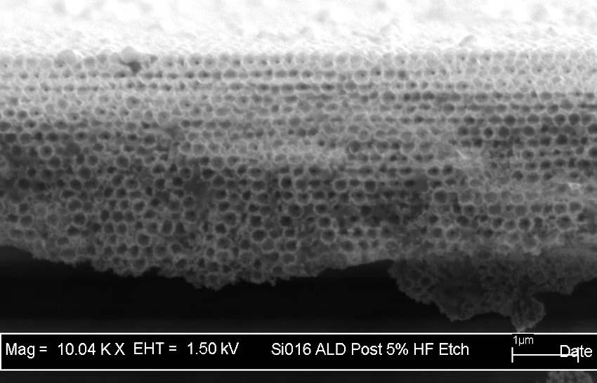
6 III. Fabrication Methodology Self-assembled thin film provides periodicity Sedimentation of monodisperse colloidal silica in a confinement cell followed by sintering to form synthetic opal (modification of method of Gates and Xia) After sintering, the opal is then infiltrated with high index material (ALD) 2% HF etch used to remove silica spheres, leaving air holes Infiltrated material must be compatible with etching scheme Self Assembly ALD Etch Sintered Opal Infiltrated Opal Inverted Opal

7 Atomic Layer Deposition Thin film grown by sequential deposition of reactants results in monolayer-by-monolayer growth Advantage: surface-controlled growth instead of source-controlled
8 Atomic Layer Deposition Available Materials: ZnS, SiO 2, TiO 2, ZnSe, Fe 2 O 3, SnS 2, GaP, W, Ta,... Multi-layered materials possible, allowing tailoring of refractive index and luminescent behavior ZnS:Mn used for initial demonstration: well studied ALD material, but insufficient index (n~2.5) for full PBG: Pseudo-gap behavior Luminescent Center: Mn 2+ doping using MnCl 2 every 100 th pulse ZnCl 2 N 2 Purge H 2 S N 2 Purge ZnCl 2 N 2 Purge H 2 S
9 IV. Characterization Methods Scanning Electron Microscopy (SEM) Film quality, conformal nature, sphere sizing Optical: Reflectivity (8 degree) lattice constant-sintered opals, filling fraction-infiltrated opals Photoluminescence (PL) Band edge and Mn 2+ excitation Crystallinity Modulation by photonic crystal Angular dependence


10 V. Results SEM ZnS:Mn Infiltrated Opal 460 nm 460 nm Sacrificial Sample Infiltrated Opal Trench Cut Via FIB
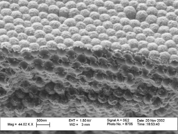
11 SEM ZnS:Mn Infiltrated/Inverse Opal d= 240 nm d= 220 nm
12 Calculation of Filling Fraction Periodicity yields Bragg diffraction Derivative of Bragg law allows calculation of (111) peak position Opals grown oriented with (111) planes parallel to substrate Resulting peak shift after infiltration allows calculation of filling fraction, f filling % for ideal FCC = f/0.26 x 100% avg λ = 2d0.816 ε avg Sin ε = ε (0.26 f ) ε + f Silica ε = avg ε silica ε. ( 0.74) ) ZnS 1 2 air θ 0.26 fε ZnS d= silica sphere diameter ε ZnS = ZnS bulk dielectric constant ε avg = effective dielectric constant θ = angle of incidence
13 Reflectivity 300 nm ZnS:Mn Opal ZnS Background subtracted Reflectivity (arb.units) nm SiO 2 OP/ZnS:Mn/ f= 90% Stand. Inf. Cond. Infiltrated 826 nm Bragg peak Reflectivity (arb. units) nm SiO 2 OPI/ZnS:Mn/ f= 94% Stand. Inf. Cond. Etched 708 nm Bragg peak Wavelength (nm) Wavelength (nm)
14 Reflectivity - Summary (111) Bragg Peak Wavelength (nm) Infiltrated Sintered Opal Opal Sphere Radius (nm) From the trendline, the average fill fraction is 90% Increased deviation as sphere size decreases Uncertainty in measurements of sphere size and wavelength d ~ 5-10 nm λ ~ 5 nm
15 PL Results ZnS:Mn Infiltrated Opal Intensity (cps) 3.50E E E E E E E+05 PL standard collection angle = 22.5º Band Edge Excitation (330 nm) 225 nm SiO 2 OP/ZnS:Mn 330 exc. f= 62.5% Stand. Inf. Cond. Cl - Mn ++ Intensity (cps) 7.00E E E E E E E+06 Mn 2+ Direct Excitation (390 nm) 225 nm SiO 2 OP/ZnS:Mn 390 exc. f= 62.5% Stand. Inf. 0.00E Wavelength 0.00E Wavelength (nm)
16 Angle Dependent PL Results ZnS:Mn Inverse Opal 2.00E E E nm SiO 2 OPI/ZnS:Mn 390exc f= 76.4% Stand. Inf. Cond. d=225 nm 10º PL Intensity (cps) 1.40E E E E E E E nm Refl. Peak º 0º 22.5º Infiltrated Detection Angle, θ 390 nm excitation 0.00E Wavelength (nm)
17 VI. Conclusions I. Successful ALD ZnS:Mn infiltration of opals Filling fractions close to 100% achieved, calculated using Reflectance SEM confirms high quality, conformal coatings II. Etched silica spheres to form inverted opal Resulting inverted opal ~ 3 5 microns thick, robust III. Luminescent Properties PL confirms high crystalline quality PL shows interesting changes, angle dependence
18 VII. Future Work I. Further optimization of ALD process for smaller opals to maximize depth of penetration of high index material II. Thorough investigation of angular dependence of reflectivity and PL III. Use ALD to fabricate inverted opals in high-n materials systems, i.e. TiO 2, Fe 2 O 3, SnS 2 GaP, etc. IV. Work on incorporation of dopant spheres in opal for microcavity fabrication
19 VIII. Acknowledgements Work supported by: U.S. Army Research Office MURI Contract# DAAA Sandia National Laboratories Contract # 18499
ATOMIC LAYER DEPOSITION FOR PHOTONIC CRYSTAL DEVICES
 ATOMIC LAYER DEPOSITION FOR PHOTONIC CRYSTAL DEVICES E. Graugnard, J. S. King, D. Heineman, and C. J. Summers School of Materials Science and Engineering, Georgia Institute of Technology, Atlanta, GA,
Luminescent and Tunable 3D Photonic Crystal Structures
 Luminescent and Tunable 3D Photonic Crystal Structures Christopher J. Summers, E. Graugnard, D. Gaillot & J. S. King School of Materials Science and Engineering Georgia Institute of Technology Atlanta,
ZnS-based photonic crystal phosphors fabricated using atomic layer deposition
 phys. stat. sol. (b) 241, No. 3, 763 766 (2004) / DOI 10.1002/pssb.200304287 ZnS-based photonic crystal phosphors fabricated using atomic layer deposition J. S. King *, 1, C. W. Neff 1, S. Blomquist 2,
Atomic layer deposition in porous structures: 3D photonic crystals
 Applied Surface Science 244 (2005) 511 516 www.elsevier.com/locate/apsusc Atomic layer deposition in porous structures: 3D photonic crystals J.S. King, D. Heineman, E. Graugnard, C.J. Summers* School of
Seminar: Structural characterization of photonic crystals based on synthetic and natural opals. Olga Kavtreva. July 19, 2005
 Seminar: Structural characterization of photonic crystals based on synthetic and natural opals Olga Kavtreva July 19, 2005 Abstract Novel class of dielectric structures with a refractive index which exhibits
Conformally Back-Filled, Non-close-packed Inverse-Opal Photonic Crystals**
 DOI: 10.1002/adma.200501077 Conformally Back-Filled, Non-close-packed Inverse-Opal Photonic Crystals** By Jeffrey S. King, Davy P. Gaillot, Elton Graugnard, and Christopher J. Summers* Photonic crystals
7-2E. Photonic crystals
 7-2E. Photonic crystals Purdue Univ, Prof. Shalaev, http://cobweb.ecn.purdue.edu/~shalaev/ Univ Central Florida, CREOL, Prof Kik, http://sharepoint.optics.ucf.edu/kik/ose6938i/handouts/forms/allitems.aspx
OPTIMIZATION OF ALD GROWN TITANIA THIN FILMS FOR THE INFILTRATION OF SILICA PHOTONIC CRYSTALS. A Dissertation Presented to The Academic Faculty
 OPTIMIZATION OF ALD GROWN TITANIA THIN FILMS FOR THE INFILTRATION OF SILICA PHOTONIC CRYSTALS A Dissertation Presented to The Academic Faculty By Dawn L. Heineman In Partial Fulfillment Of the Requirements
Sacrificial-Layer Atomic Layer Deposition for Fabrication of Non- Close-Packed Inverse-Opal Photonic Crystals**
 DOI: 10.1002/adfm.200500841 Sacrificial-Layer Atomic Layer Deposition for Fabrication of Non- Close-Packed Inverse-Opal Photonic Crystals** By Elton Graugnard, Jeffrey S. King, Davy P. Gaillot, and Christopher
Versatile multi-layered metal-oxide inverse opal fabrication for photocatalytic applications
 Versatile multi-layered metal-oxide inverse opal fabrication for photocatalytic applications Delphine Lebrun Div. Solid state physics Dep. Engineering Sciences Uppsala University Sweden Versatile multi-layered
Plasmonics using Metal Nanoparticles. Tammy K. Lee and Parama Pal ECE 580 Nano-Electro-Opto-Bio
 Plasmonics using Metal Nanoparticles Tammy K. Lee and Parama Pal ECE 580 Nano-Electro-Opto-Bio April 1, 2007 Motivation Why study plasmonics? Miniaturization of optics and photonics to subwavelength scales
Red luminescence from Si quantum dots embedded in SiO x films grown with controlled stoichiometry
 Red luminescence from Si quantum dots embedded in films grown with controlled stoichiometry Zhitao Kang, Brannon Arnold, Christopher Summers, Brent Wagner Georgia Institute of Technology, Atlanta, GA 30332
Self-Assembled 3d Photonic Crystals For Applications In Optical Communications
 Self-Assembled 3d Photonic Crystals For Applications In Optical Communications Giulia Smonker Departamento de Engenharia de Materiais, Instituto Superior Técnico, Av. Rovisco Pais,1049-001 Lisboa, Portugal
Cristaux 3D. Fabriquer de tels objets aux longueur d'ondes optiques???
 Cristaux 3D Fabriquer de tels objets aux longueur d'ondes optiques??? A la main, une sphère l'une après l'autre... 5μm 5μm dissolve latex spheres 4-layer [111] silica diamond lattice 6-layer [001] silica
Atomic Layer Deposition (ALD)
") Atomic Layer Deposition (ALD) ALD provides Uniform, controlled, conformal deposition of oxide, nitride, and metal thin films on a nanometer scale. ALD is a self limiting thin film deposition technique
Atomic Layer Deposition (ALD) ALD provides Uniform, controlled, conformal deposition of oxide, nitride, and metal thin films on a nanometer scale. ALD is a self limiting thin film deposition technique
Lecture 22: Integrated circuit fabrication
 Lecture 22: Integrated circuit fabrication Contents 1 Introduction 1 2 Layering 4 3 Patterning 7 4 Doping 8 4.1 Thermal diffusion......................... 10 4.2 Ion implantation.........................
Supplementary Information
 Supplementary Information for Embedded Cavities and Waveguides in 3D Silicon Photonic Crystals by S. A. Rinne, F. García-Santamaría, and P. V. Braun, Nature Photonics, 2007 Figure S1. Figure S1 Detailed
Silver Diffusion Bonding and Layer Transfer of Lithium Niobate to Silicon
 Chapter 5 Silver Diffusion Bonding and Layer Transfer of Lithium Niobate to Silicon 5.1 Introduction In this chapter, we discuss a method of metallic bonding between two deposited silver layers. A diffusion
Optical parameter determination of ZrO 2 thin films prepared by sol gel dip coating
 International Journal of ChemTech Research CODEN (USA): IJCRGG ISSN : 0974-490 Vol.6, No.13, pp 534-5346, November 014 MESCon 014 [4th -5 th September 014] National Conference on Material for Energy Storage
Application of INAA for Aluminium Magnesium Oxide Materials Investigation
 Application of INAA for Aluminium Magnesium Oxide Materials Investigation D. Riekstina, O. Veveris, V. Skvortsova, Institute of Solid State Physics, University of Latvia APPLICATIONS T melt = 2800ºC ccubic
Solar Cells and Photosensors.
 Designing Photonic Crystals in Strongly Absorbing Material for Applications in Solar Cells and Photosensors. Minda Wagenmaker 1, Ebuka S. Arinze 2, Botong Qiu 2, Susanna M. Thon 2 1 Mechanical Engineering
ALD of Scandium Oxide from Tris(N,N -diisopropylacetamidinato)scandium and Water
scandium and Water") ALD of Scandium Oxide from Tris(N,N -diisopropylacetamidinato)scandium and Water Philippe P. de Rouffignac, Roy G. Gordon Dept. of Chemistry,, Cambridge, MA gordon@chemistry.harvard.edu (617) 495-4017
ALD of Scandium Oxide from Tris(N,N -diisopropylacetamidinato)scandium and Water Philippe P. de Rouffignac, Roy G. Gordon Dept. of Chemistry,, Cambridge, MA gordon@chemistry.harvard.edu (617) 495-4017
Synthesis and Characterization of Zinc Iron Sulphide (ZnFeS) Of Varying Zinc Ion Concentration
 Of Varying Zinc Ion Concentration") International Journal of Science and Technology Volume 5 No. 5, May, 2016 Synthesis and Characterization of Zinc Iron Sulphide (ZnFeS) Of Varying Zinc Ion Concentration I. B. Obasi 1 and J. C. Osuwa 2
International Journal of Science and Technology Volume 5 No. 5, May, 2016 Synthesis and Characterization of Zinc Iron Sulphide (ZnFeS) Of Varying Zinc Ion Concentration I. B. Obasi 1 and J. C. Osuwa 2
TED PELLA, INC. Microscopy Products for Science and Industry
 PELCO SILICON NITRIDE, SILICON DIOXIDE, BLANK SILICON SUBSTRATES & APERTURES FOR TEM Clean, Debris-free with Exact 3mm TEM Frame and EasyGrip Edges PELCO Silicon Nitride Support Films for TEM Hydrophilic
This lecture is part of the Basic XRD Course.
 This lecture is part of the Basic XRD Course. Basic XRD Course 1 A perfect polycrystalline sample should contain a large number of crystallites. Ideally, we should always be able to find a set of crystallites
Dielectric II-VI and IV-VI Metal Chalcogenide Thin Films in Hollow Glass Waveguides (HGWs) for Infrared Spectroscopy and Laser Delivery
 for Infrared Spectroscopy and Laser Delivery") Dielectric II-VI and IV-VI Metal Chalcogenide Thin Films in Hollow Glass Waveguides (HGWs) for Infrared Spectroscopy and Laser Delivery Carlos M. Bledt * a, Daniel V. Kopp a, and James A. Harrington a
Dielectric II-VI and IV-VI Metal Chalcogenide Thin Films in Hollow Glass Waveguides (HGWs) for Infrared Spectroscopy and Laser Delivery Carlos M. Bledt * a, Daniel V. Kopp a, and James A. Harrington a
Lecture 5. SOI Micromachining. SOI MUMPs. SOI Micromachining. Silicon-on-Insulator Microstructures. Agenda:
 EEL6935 Advanced MEMS (Spring 2005) Instructor: Dr. Huikai Xie SOI Micromachining Agenda: SOI Micromachining SOI MUMPs Multi-level structures Lecture 5 Silicon-on-Insulator Microstructures Single-crystal
How can we describe a crystal?
 How can we describe a crystal? Examples of common structures: (1) The Sodium Chloride (NaCl) Structure (LiH, MgO, MnO, AgBr, PbS, KCl, KBr) The NaCl structure is FCC The basis consists of one Na atom and
Multilayer Silver / Dielectric Thin-Film Coated Hollow Waveguides for Sensor and Laser Power Delivery Applications
 Multilayer Silver / Dielectric Thin-Film Coated Hollow Waveguides for Sensor and Laser Power Delivery Applications Theory, Design, and Fabrication Carlos M. Bledt a, James A. Harrington a, and Jason M.
Spectrometer gratings based on direct-write e-beam lithography
 Spectrometer gratings based on direct-write e-beam lithography U.D. Zeitner, T. Flügel-Paul, T. Harzendorf, M. Heusinger, E.-B. Kley Fraunhofer Institut für Angewandte Optik und Feinmechanik Jena, Germany
Assembly of Highly Ordered Three-Dimensional Porous Structure with Nanocrystalline TiO 2 Semiconductors
 Chem. Mater. 2002, 14, 83-88 83 Assembly of Highly Ordered Three-Dimensional Porous Structure with Nanocrystalline TiO 2 Semiconductors Q.-B. Meng,*,, C.-H. Fu, Y. Einaga, Z.-Z. Gu, A. Fujishima,, and
Structural and Optical Properties of MnO 2 : Pb Nanocrystalline Thin Films Deposited By Chemical Spray Pyrolysis
 IOSR Journal of Engineering (IOSRJEN) e-issn: 2250-3021, p-issn: 2278-8719 Vol. 3, Issue 4 (April. 2013), V4 PP 52-57 Structural and Optical Properties of MnO 2 : Pb Nanocrystalline Thin Films Deposited
Supplementary Information
 Supplementary Information Supplementary Figure 1 Characterization of precursor coated on salt template. (a) SEM image of Mo precursor coated on NaCl. Scale bar, 50 μm. (b) EDS of Mo precursor coated on
STRUCTURAL AND OPTOELECTRONIC PROPERTIES OF PYRALYTICALLY SPRAYED CdZnS THIN FILMS
 Chalcogenide Letters Vol. 9, No. 12, December 2012, p. 495-500 STRUCTURAL AND OPTOELECTRONIC PROPERTIES OF PYRALYTICALLY SPRAYED CdZnS THIN FILMS S. RAJATHI *, N. SANKARASUBRAMANIAN *, K. RAMANATHAN, M.
Low-cost, deterministic quasi-periodic photonic structures for light trapping in thin film silicon solar cells
 Low-cost, deterministic quasi-periodic photonic structures for light trapping in thin film silicon solar cells The MIT Faculty has made this article openly available. Please share how this access benefits
Fabrication of annular photonic crystals by atomic layer deposition and sacrificial etching
 Fabrication of annular photonic crystals by atomic layer deposition and sacrificial etching Junbo Feng School of Optoelectronics Science and Engineering, Wuhan National Laboratory for Optoelectronics,
Effect of Doping Concentration on the Structural Properties of Zn: SnO 2
 IOSR Journal of Applied Physics (IOSR-JAP) e-issn: 2278-4861.Volume 7, Issue 3 Ver. II (May. - Jun. 2015), PP 45-49 www.iosrjournals.org Effect of Doping Concentration on the Structural Properties of Zn:
Dispersion characteristics of silicon nanorod based carpet cloaks
 Dispersion characteristics of silicon nanorod based carpet cloaks Venkata A. Tamma 1, John Blair 2, Christopher J. Summers 2 and Wounjhang Park 1* 1 Department of Electrical, Computer & Energy Engineering,
Department of Applied Chemistry, Faculty of Science and Technology, Keio University,
 Sol-gel preparation and luminescent properties of CeO 2 :Ln (Ln = Eu 3+ and Sm 3+ ) thin films Masashi Oikawa, Shinobu Fujihara *, Toshio Kimura Department of Applied Chemistry, Faculty of Science and
The growth of patterned ceramic thin films from polymer precursor solutions Göbel, Ole
 University of Groningen The growth of patterned ceramic thin films from polymer precursor solutions Göbel, Ole IMPORTANT NOTE: You are advised to consult the publisher's version (publisher's PDF) if you
Introduction to Lithography
 Introduction to Lithography G. D. Hutcheson, et al., Scientific American, 290, 76 (2004). Moore s Law Intel Co-Founder Gordon E. Moore Cramming More Components Onto Integrated Circuits Author: Gordon E.
Manipulation and control of spatial ALD layers for flexible devices. Aimcal Memphis 2016; Edward Clerkx
 Manipulation and control of spatial ALD layers for flexible devices Meyer Burger Netherlands Equipment manufacturer Functional inkjet printing Based in Eindhoven, the Netherlands Part of world-wide Meyer
Synthesis of inverse opals
 Colloids and Surfaces A: Physicochemical and Engineering Aspects 202 (2002) 281 290 www.elsevier.com/locate/colsurfa Synthesis of inverse opals F. Meseguer a,b, *, A. Blanco a,b,h.míguez a,b, F. García-Santamaría
INTEGRATED OPTICAL ISOLATOR
 INTEGRATED OPTICAL ISOLATOR Presented by Gokhan Ozgur Advisor: Dr. Gary Evans July 02, 2004 Electrical Engineering - SMU INTRODUCTION They are used to eliminate light that is back-reflected, from splices
BBO Crystals. Features. Broad phase-matchable second-harmonic-generation (SHG) range from nm to 2500 nm
 range from nm to 2500 nm") BBO Crystals Broad phase-matchable second-harmonic-generation (SHG) range from 409.6 nm to 2500 nm Wide transparency range from 189 nm to 2600 nm High damage threshold of 10 J/cm 2 for 10 ns pulse-width
BBO Crystals Broad phase-matchable second-harmonic-generation (SHG) range from 409.6 nm to 2500 nm Wide transparency range from 189 nm to 2600 nm High damage threshold of 10 J/cm 2 for 10 ns pulse-width
High Pressure Chemical Vapor Deposition to make Multimaterial Optical Fibers
 High Pressure Chemical Vapor Deposition to make Multimaterial Optical Fibers Subhasis Chaudhuri *1 1, 2, 3, John V. Badding 1 Department of Chemistry, Pennsylvania State University, University Park, PA
Chapter 3 Basic Crystallography and Electron Diffraction from Crystals. Lecture 9. Chapter 3 CHEM Fall, L. Ma
 Chapter 3 Basic Crystallography and Electron Diffraction from Crystals Lecture 9 Outline The geometry of electron diffraction Crystallography Kinetic Theory of Electron diffraction Diffraction from crystals
HOMEWORK 4 and 5. March 15, Homework is due on Monday March 30, 2009 in Class. Answer the following questions from the Course Textbook:
 HOMEWORK 4 and 5 March 15, 2009 Homework is due on Monday March 30, 2009 in Class. Chapter 7 Answer the following questions from the Course Textbook: 7.2, 7.3, 7.4, 7.5, 7.6*, 7.7, 7.9*, 7.10*, 7.16, 7.17*,
CHAPTER 8 CONCLUSIONS AND SCOPE FOR FUTURE WORK
 CHAPTER 8 CONCLUSIONS AND SCOPE FOR FUTURE WORK In this thesis an experimental investigation about Magnisium oxide (MgO) nanoparticles and its nanocomposites i.e.mgo-x (X= NiO, CuO, Co3O4, Fe2O3, CeO2,
EFFECT OF CRYSTALORIENTATIONIN OXIDATION PROCESS OF VLSI FABRICATION
 International Journal of Research in Engineering, Technology and Science, Volume VII, Special Issue, Feb 2017 www.ijrets.com, editor@ijrets.com, ISSN 2454-1915 EFFECT OF CRYSTALORIENTATIONIN OXIDATION
Femtosecond micromachining in polymers
 Femtosecond micromachining in polymers Prof. Dr Cleber R. Mendonca Daniel S. Corrêa Prakriti Tayalia Dr. Tobias Voss Dr. Tommaso Baldacchini Prof. Dr. Eric Mazur fs-micromachining focus laser beam inside
9/4/2008 GMU, ECE 680 Physical VLSI Design
 ECE680: Physical VLSI Design Chapter II CMOS Manufacturing Process 1 Dual-Well Trench-Isolated CMOS Process gate-oxide TiSi 2 AlCu Tungsten SiO 2 p-well poly n-well SiO 2 n+ p-epi p+ p+ 2 Schematic Layout
PROJECT PERIODIC REPORT
 PROJECT PERIODIC REPORT Grant Agreement number: 619456 Project acronym: SITOGA Project title: Silicon CMOS compatible transition metal oxide technology for boosting highly integrated photonic devices with
Modified spontaneous emission from erbium-doped photonic layer-by-layer crystals
 PHYSICAL REVIEW B 67, 115106 2003 Modified spontaneous emission from erbium-doped photonic layer-by-layer crystals M. J. A. de Dood* and A. Polman FOM Institute for Atomic and Molecular Physics, Kruislaan
ZnO thin film deposition on sapphire substrates by chemical vapor deposition
 ZnO thin film deposition on sapphire substrates by chemical vapor deposition Zhuo Chen 1, T. Salagaj 2, C. Jensen 2, K. Strobl 2, Mim Nakarmi 1, and Kai Shum 1, a 1 Physics Department, Brooklyn College
Polymer-based optical interconnects using nano-imprint lithography
 Polymer-based optical interconnects using nano-imprint lithography Arjen Boersma,Sjoukje Wiegersma Bert Jan Offrein, Jeroen Duis, Jos Delis, Markus Ortsiefer, Geert van Steenberge, MikkoKarppinen, Alfons
Raman and Er-doped Microlasers on a Si chip by Solgel Method
 Raman and Er-doped Microlasers on a Si chip by Solgel Method Lan Yang, Sean Spillane, Bumki Min, Tal Carmon and Kerry Vahala Department of Applied Physics California Institute of Technology 1 Outline Introduction
Potassium Titanyl Phosphate (KTP) Crystals
 Crystals") CASIX, Inc. Crystals Potassium Titanyl Phosphate (KTP) Crystals CASIX s KTP crystals feature high purity, low absorption at fundamental and second harmonic generation wavelengths. We supply super grade
CASIX, Inc. Crystals Potassium Titanyl Phosphate (KTP) Crystals CASIX s KTP crystals feature high purity, low absorption at fundamental and second harmonic generation wavelengths. We supply super grade
Example: Compute the wavelength of a 1 [kg] block moving at 1000 [m/s].
![Example: Compute the wavelength of a 1 [kg] block moving at 1000 [m/s].](/thumbs/95/123245062.jpg "Example: Compute the wavelength of a 1 [kg] block moving at 1000 [m/s].") Example: Calculate the energy required to excite the hydrogen electron from level n = 1 to level n = 2. Also calculate the wavelength of light that must be absorbed by a hydrogen atom in its ground state
Example: Calculate the energy required to excite the hydrogen electron from level n = 1 to level n = 2. Also calculate the wavelength of light that must be absorbed by a hydrogen atom in its ground state
Supplementary Information. for
 Electronic Supplementary Material (ESI) for ChemComm. This journal is The Royal Society of Chemistry 2014 Supplementary Information for Nanoslitting Phase-separated Block Copolymers by Solvent Swelling
Research Article Optical Properties and Characterization of Prepared Sn-Doped PbSe Thin Film
 Condensed Matter Physics Volume 1, Article ID 58743, 4 pages doi:1.1155/1/58743 Research Article Optical Properties and Characterization of Prepared Sn-Doped PbSe Thin Film M. R. Khanlary 1, and E. Salavati
CHAPTER 2. EFFECT OF COBALT DOPING ON THE STRUCTURAL AND OPTICAL PROPERTIES OF TiO 2 FILMS PREPARED BY SOL-GEL PROCESS
 3 CHAPTER EFFECT OF COBALT DOPING ON THE STRUCTURAL AND OPTICAL PROPERTIES OF TiO FILMS PREPARED BY SOL-GEL PROCESS.1 INTRODUCTION Titanium dioxide (TiO ) thin films possess high transmittance and high
Ultra High Barrier Coatings by PECVD
 Society of Vacuum Coaters 2014 Technical Conference Presentation Ultra High Barrier Coatings by PECVD John Madocks & Phong Ngo, General Plasma Inc., 546 E. 25 th Street, Tucson, Arizona, USA Abstract Silicon
A High Speed Surface Illuminated Si Photodiode. Using Microstructured Holes for Absorption. Enhancements at nm wavelength
 A High Speed Surface Illuminated Si Photodiode Using Microstructured Holes for Absorption Enhancements at 900 1000 nm wavelength Supporting Information Yang Gao, Hilal Cansizoglu, Soroush Ghandiparsi,
Transmission Mode Photocathodes Covering the Spectral Range
 Transmission Mode Photocathodes Covering the Spectral Range 6/19/2002 New Developments in Photodetection 3 rd Beaune Conference June 17-21, 2002 Arlynn Smith, Keith Passmore, Roger Sillmon, Rudy Benz ITT
CHAPTER 4. SYNTHESIS OF ALUMINIUM SELENIDE (Al 2 Se 3 ) NANO PARTICLES, DEPOSITION AND CHARACTERIZATION
 NANO PARTICLES, DEPOSITION AND CHARACTERIZATION") 40 CHAPTER 4 SYNTHESIS OF ALUMINIUM SELENIDE (Al 2 Se 3 ) NANO PARTICLES, DEPOSITION AND CHARACTERIZATION 4.1 INTRODUCTION Aluminium selenide is the chemical compound Al 2 Se 3 and has been used as a precursor
40 CHAPTER 4 SYNTHESIS OF ALUMINIUM SELENIDE (Al 2 Se 3 ) NANO PARTICLES, DEPOSITION AND CHARACTERIZATION 4.1 INTRODUCTION Aluminium selenide is the chemical compound Al 2 Se 3 and has been used as a precursor
Damage Threats and Response of Final Optics for Laser-Fusion Power Plants
 Damage Threats and Response of Final Optics for Laser-Fusion Power Plants M. S. Tillack 1, S. A. Payne 2, N. M. Ghoniem 3, M. R. Zaghloul 1 and J. F. Latkowski 2 1 UC San Diego, La Jolla, CA 92093-0417
Fundamentals of X-ray diffraction and scattering
 Fundamentals of X-ray diffraction and scattering Don Savage dsavage@wisc.edu 1231 Engineering Research Building (608) 263-0831 X-ray diffraction and X-ray scattering Involves the elastic scattering of
Chapter 7 NANOIMPRINTED CIRCULAR GRATING DISTRIBUTED FEEDBACK DYE LASER
 Chapter 7 66 NANOIMPRINTED CIRCULAR GRATING DISTRIBUTED FEEDBACK DYE LASER 7.1 Introduction In recent years, polymer dye lasers have attracted much attention due to their low-cost processing, wide choice
Supplementary Figure 1 TEM of external salt byproducts. TEM image of some salt byproducts precipitated out separately from the Si network, with
 Supplementary Figure 1 TEM of external salt byproducts. TEM image of some salt byproducts precipitated out separately from the Si network, with non-uniform particle size distribution. The scale bar is
Hydrogenated Amorphous Silicon Nitride Thin Film as ARC for Solar Cell Applications
 ISSN 2278 211 (Online) Hydrogenated Amorphous Silicon Nitride Thin Film as ARC for Solar Cell Applications Dr. G. Natarajan Professor & Head, Department of Physics PSNA College of Engineering and Technology,
Metodi di fabbricazione PhC
 Metodi di fabbricazione PhC PhC in 1D a n 1 n 2 z Deposizione multilayer (MBE,MOCVD,PVD,CVD) Silicio poroso Litografia Crescita per deposizione Physical deposition Chemical deposition InP by MOCVD Deposizione
Czochralski Crystal Growth
 Czochralski Crystal Growth Crystal Pulling Crystal Ingots Shaping and Polishing 300 mm wafer 1 2 Advantage of larger diameter wafers Wafer area larger Chip area larger 3 4 Large-Diameter Wafer Handling
Coatings. Ion Assisted Deposition (IAD) process Advance Plasma Source (APS) plasma-ion assisted Deposition. Coatings on Optical Fibers
 process Advance Plasma Source (APS) plasma-ion assisted Deposition. Coatings on Optical Fibers") Anti-Reflection Custom Ion Assisted Deposition (IAD) process Advance Plasma Source (APS) plasma-ion assisted Deposition Anti-Reflection on Optical Fibers OptoSigma supplies a wide selection of optical
Anti-Reflection Custom Ion Assisted Deposition (IAD) process Advance Plasma Source (APS) plasma-ion assisted Deposition Anti-Reflection on Optical Fibers OptoSigma supplies a wide selection of optical
Microfabrication of Integrated Circuits
 Microfabrication of Integrated Circuits OUTLINE History Basic Processes Implant; Oxidation; Photolithography; Masks Layout and Process Flow Device Cross Section Evolution Lecture 38, 12/05/05 Reading This
Complexity of IC Metallization. Early 21 st Century IC Technology
 EECS 42 Introduction to Digital Electronics Lecture # 25 Microfabrication Handout of This Lecture. Today: how are Integrated Circuits made? Silicon wafers Oxide formation by growth or deposition Other
Fabrication of photonic band-gap crystals
 Fabrication of photonic band-gap crystals C. C. Cheng and A. Scherer California Institute of Technology, Pasadena, California 91125 Received 19 June 1995; accepted 9 August 1995 We describe the fabrication
High Density Iron Silicide Nanodots Formed by Ultrathin SiO 2 Film Technique
 Available online at www.sciencedirect.com Procedia Engineering 36 (2012 ) 382 387 IUMRS-ICA 2011 High Density Iron Silicide Nanodots Formed by Ultrathin SiO 2 Film Technique Yoshiaki Nakamura a,b* a Graduate
EECS130 Integrated Circuit Devices
 EECS130 Integrated Circuit Devices Professor Ali Javey 9/13/2007 Fabrication Technology Lecture 1 Silicon Device Fabrication Technology Over 10 15 transistors (or 100,000 for every person in the world)
Influence of In/Sn ratio on nanocrystalline indium tin oxide thin films by spray pyrolysis method
 Available online at www.scholarsresearchlibrary.com Scholars Research Library Archives of Physics Research, 2011, 2 (1): 19-25 (http://scholarsresearchlibrary.com/archive.html) ISSN 0976-0970 CODEN (USA):
Silicon Rich Silicon Oxide Thin Films Fabricated by Electro-Chemical Method
 Silicon Rich Silicon Oxide Thin Films Fabricated by Electro-Chemical Method Pham Van Hoi, Do Thuy Chi, Bui Huy and Nguyen Thuy Van Vietnam Academy of Science and Technology, Vietnam 2 1. Introduction Porous
A discussion of crystal growth, lithography, etching, doping, and device structures is presented in
 Chapter 5 PROCESSING OF DEVICES A discussion of crystal growth, lithography, etching, doping, and device structures is presented in the following overview gures. SEMICONDUCTOR DEVICE PROCESSING: AN OVERVIEW
2Dlayer Product Catalog
 2Dlayer Product Catalog Your idea, Our materials! We provide solutions, not just materials. Tel.: 1-919-228-9662 Email: info@2dlayer.com URL: http://2dlayer.com We accept purchase orders and all kinds
Lecture 19 Microfabrication 4/1/03 Prof. Andy Neureuther
 EECS 40 Spring 2003 Lecture 19 Microfabrication 4/1/03 Prof. ndy Neureuther How are Integrated Circuits made? Silicon wafers Oxide formation by growth or deposition Other films Pattern transfer by lithography
Optical Properties of Nanocrystalline Silicon Thin Films in Wider Regions of Wavelength
 Optical Properties of Nanocrystalline Silicon Thin Films in Wider Regions of Wavelength Tarjudin, N.A. 1,*, Sumpono, I 1, Sakrani, S 2. 1 Institut Ibnu Sina, 2 Jabatan Fizik, Fakulti Sains, Universiti
1. Introduction. What is implantation? Advantages
 Ion implantation Contents 1. Introduction 2. Ion range 3. implantation profiles 4. ion channeling 5. ion implantation-induced damage 6. annealing behavior of the damage 7. process consideration 8. comparison
EE40 Lec 22. IC Fabrication Technology. Prof. Nathan Cheung 11/19/2009
 Suggested Reading EE40 Lec 22 IC Fabrication Technology Prof. Nathan Cheung 11/19/2009 300mm Fab Tour http://www-03.ibm.com/technology/manufacturing/technology_tour_300mm_foundry.html Overview of IC Technology
لبا ب ةعماج / ةيساسلأا ةيبرتلا ةيلك ة لجم
 Photoluminescence from Etched Silicon Surface by High Power Laser Oday A. Abbass Department of Physics/College of Sciences/University of Kufa ABSTRACT Porous silicon layers (P-Si) has been prepared in
EE 143 FINAL EXAM NAME C. Nguyen May 10, Signature:
 INSTRUCTIONS Read all of the instructions and all of the questions before beginning the exam. There are 5 problems on this Final Exam, totaling 143 points. The tentative credit for each part is given to
3. Monodomain porous alumina obtained by nanoimprint lithography
 3. Monodomain porous alumina obtained by nanoimprint lithography 3.1 Nanoimprint lithography (NIL) In the previous chapter, the preparation of polydomain porous alumina by self-ordering was discussed.
EUV Transmission Lens Design and Manufacturing Method
 1 EUV Transmission Lens Design and Manufacturing Method Kenneth C. Johnson kjinnovation@earthlink.net 7/16/2018 http://vixra.org/abs/1807.0188 Abstract This paper outlines a design for an EUV transmission
Supplementary Figure S1 Photograph of MoS 2 and WS 2 flakes exfoliated by different metal naphthalenide (metal = Na, K, Li), and dispersed in water.
, and dispersed in water.") Supplementary Figure S1 Photograph of MoS 2 and WS 2 flakes exfoliated by different metal naphthalenide (metal = Na, K, Li), and dispersed in water. Supplementary Figure S2 AFM measurement of typical LTMDs
Supplementary Figure S1 Photograph of MoS 2 and WS 2 flakes exfoliated by different metal naphthalenide (metal = Na, K, Li), and dispersed in water. Supplementary Figure S2 AFM measurement of typical LTMDs
Amorphous silicon waveguides for microphotonics
 4 Amorphous silicon waveguides for microphotonics Amorphous silicon a-si was made by ion irradiation of crystalline silicon with 1 10 15 Xe ions cm 2 at 77 K in the 1 4 MeV energy range. Thermal relaxation
Bulk crystal growth. A reduction in Lg will increase g m and f oper but with some costs
 Bulk crystal growth The progress of solid state device technology has depended not only on the development of device concepts but also on the improvement of materials. A reduction in Lg will increase g
Growth and formation of inverse GaP and InP opals
 Growth and formation of inverse GaP and InP opals Yates, HM, Whitehead, DE, Nolan, MG, Pemble, ME, Palacios Lidón, E, Rubio, S, Meseguer, FJ and López, C Title Growth and formation of inverse GaP and InP
An advantage of thin-film silicon solar cells is that they can be deposited on glass substrates and flexible substrates.
 ET3034TUx - 5.2.1 - Thin film silicon PV technology 1 Last week we have discussed the dominant PV technology in the current market, the PV technology based on c-si wafers. Now we will discuss a different
PROCESS FLOW AN INSIGHT INTO CMOS FABRICATION PROCESS
 Contents: VI Sem ECE 06EC63: Analog and Mixed Mode VLSI Design PROCESS FLOW AN INSIGHT INTO CMOS FABRICATION PROCESS 1. Introduction 2. CMOS Fabrication 3. Simplified View of Fabrication Process 3.1 Alternative
Structure and optical properties of M/ZnO (M=Au, Cu, Pt) nanocomposites
 nanocomposites") Solar Energy Materials & Solar Cells 8 () 339 38 Structure and optical properties of M/ (M=Au, Cu, Pt) nanocomposites U. Pal a,b, *, J. Garc!ıa-Serrano a, G. Casarrubias-Segura a, N. Koshizaki c, T. Sasaki
Solar Energy Materials & Solar Cells 8 () 339 38 Structure and optical properties of M/ (M=Au, Cu, Pt) nanocomposites U. Pal a,b, *, J. Garc!ıa-Serrano a, G. Casarrubias-Segura a, N. Koshizaki c, T. Sasaki
PATTERNING OF OXIDE THIN FILMS BY UV-LASER ABLATION
 Journal of Optoelectronics and Advanced Materials Vol. 7, No. 3, June 2005, p. 1191-1195 Invited lecture PATTERNING OF OXIDE THIN FILMS BY UV-LASER ABLATION J. Ihlemann * Laser-Laboratorium Göttingen e.v.,
162 Solar Energy. front contact (metal grid) serial connections (to the back contact of the next cell) p-type wafer back contact
 serial connections (to the back contact of the next cell) p-type wafer back contact") 162 Solar Energy serial connections (to the back contact of the next cell) front contact (metal grid) antireflective coating n + -type emitter p + -type layer p-type wafer back contact 200 μm Figure 12.8:
162 Solar Energy serial connections (to the back contact of the next cell) front contact (metal grid) antireflective coating n + -type emitter p + -type layer p-type wafer back contact 200 μm Figure 12.8: