Regents of the University of California 1
|
|
|
- Suzanna Cole
- 5 years ago
- Views:
Transcription

1 Electroplating: Metal MEMS Nickel Surface-Micromachining Process Flow Photoresist Wafer Release Etchant Use electroplating to obtain metal μstructures When thick: call it LIGA Pros: fast low temp deposition, very conductive Cons: drift, low mech. Q but may be solvable? Electrode Suspended Nickel Microstructure Nickel Ti/Au EE C245: Introduction to MEMS Design LecM 5 C. Nguyen 8/20/09 35 Si 3 N 4 Isolation EE C245: Introduction to MEMS Design LecM 5 C. Nguyen 8/20/09 36 Nickel Metal Surface-Micromachining Nickel Metal Surface-Micromachining Oxide Photoresist Titanium Titanium Gold Gold Deposit isolation LTO: Target = 2μm 1 hr. 40 min. o C Densify the LTO o C for 30 min. Define metal interconnect via lift-off Spin photoresist and pattern lithographically to open areas where interconnect will stay Evaporate a Ti/Au layer Target = 30nm Ti Target = 270nm Au Remove photoresist in PRS2000 Ti/Au atop the photoresist also removed EE C245: Introduction to MEMS Design LecM 5 C. Nguyen 8/20/09 37 Photoresist Evaporate Al to serve as a sacrificial layer Target = 1μm Lithography to define anchor openings Wet etch the aluminum to form anchor vias Use solution of H 3 PO 4 /HNO 3 /H 2 O Remove photoresist in PRS2000 Electroplate nickel to fill the anchor vias Use solution of nickel 50 C Time the electroplating to planarize the surface EE C245: Introduction to MEMS Design LecM 5 C. Nguyen 8/20/

2 Nickel Metal Surface-Micromachining Nickel Metal Surface-Micromachining Nickel seed layer Photoresist Electroplated Nickel Evaporate a thin film of nickel to serve as a seed layer for subsequent Ni electroplating Target = 20nm Form a photoresist mold for subsequent electroplating Spin 6 um-thick AZ 9260 photoresist Lithographically pattern the photoresist to delineate areas where nickel structures are to be formed Electroplate nickel structural material through the PR mold Use a solution of nickel 50 o C Cathode-to-anode current density ~ 2.5 ma/cm 2 Electroplated Nickel Electroplated Nickel Strip the PR in PRS2000 Remove the Ni seed layer in Ni wet etchant Release the structures Use a K 4 Fe(CN) 6 /NaOH etchant that attacks Al while leaving Ni and Au intact Etch selectivity > 100:1 for Al:Ni and Al:Au EE C245: Introduction to MEMS Design LecM 5 C. Nguyen 8/20/09 39 EE C245: Introduction to MEMS Design LecM 5 C. Nguyen 8/20/09 40 Nickel Surface-Micromachining Example Below: Surface-micromachined in nickel using the described process flow 3D Pop-up MEMS EE C245: Introduction to MEMS Design LecM 5 C. Nguyen 8/20/09 41 EE C245: Introduction to MEMS Design LecM 5 C. Nguyen 8/20/

![, 1992] Pop-Up MEMS Pictured:](/docs-images/83/88392997/images/3-1.jpg "hinged Campanile made in")

![al.] Corner Cube Reflector [v.](/docs-images/83/88392997/images/3-3.jpg "Hsu, 1999] EE C245:")


![UCLA] EE C245: Nguyen](/docs-images/83/88392997/images/3-7.jpg "8/20/09 45 EE C245: Nguyen")
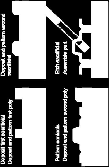
3 Pop-Up MEMS First MEMS hinge [K. Pister, et al., 1992] Pop-Up MEMS Pictured: hinged Campanile made in SUMMiT process, assembled using probes [Elliot Hui, et al.] Corner Cube Reflector [v. Hsu, 1999] EE C245: Introduction to MEMS Design LecM 5 C. Nguyen 8/20/09 43 EE C245: Introduction to MEMS Design LecM 5 C. Nguyen 8/20/ D Direct-Assembled Tunable L Hinge Process Flow [Ming Wu, UCLA] EE C245: Introduction to MEMS Design LecM 5 C. Nguyen 8/20/09 45 EE C245: Introduction to MEMS Design LecM 5 C. Nguyen 8/20/
 now owned")


: in layout, boxes represent features that will stay through")

4 MUMPS: MultiUser MEMS ProcesS Foundry MEMS: The MUMPS Process Originally created by the Microelectronics Center of North Carolina (MCNC) now owned by MEMSCAP in France Three-level polysilicon surface micromachining process for prototyping and foundry services Designed to service as many users as possible; basically an attempt to provide a universal MEMS process 8 photomasks $4,900 for 1 cm 2 dies Micromotor fabricated via MUMPS EE C245: Introduction to MEMS Design LecM 5 C. Nguyen 8/20/09 47 EE C245: Introduction to MEMS Design LecM 5 C. Nguyen 8/20/09 48 MUMPS: MultiUser MEMS ProcesS Micromotor Example Minimum set set of of masks that must be be used in in MUMPS Masks in polymumps EE C245: Introduction to MEMS Design LecM 5 C. Nguyen 8/20/09 49 Extra masks for for more Field type: flexibility & ease of of release Light (or clear) field (cf): in layout, boxes represent features that will stay through fabrication Dark field (df): in layout, boxes represent holes to be cut out EE C245: Introduction to MEMS Design LecM 5 C. Nguyen 8/20/
 Deposit PSG on the starting n- type (100) wafers Anneal to heavily dope the wafers")
 mask and RIE etching to pattern the poly0 ground plane layer LPCVD 2")
 RIE 750 nm deep to form dimple vias Lithography using the ANCHOR1 (df) mask (align")


 Recoat with photoresist and do lithography using the ANCHOR2(df) mask to define")


 (as an adhesion layer for gold) Evaporate gold (Au) Liftoff to remove PR")
5 MUMPS Process Flow MUMPS Process Flow (cont.) Deposit PSG on the starting n- type (100) wafers Anneal to heavily dope the wafers Remove the PSG LPCVD 600 nm of low stress nitride LPCVD 500 nm of polysilicon Lithography using the POLY0(cf) mask and RIE etching to pattern the poly0 ground plane layer LPCVD 2 μm of PSG as the 1 st sacrificial layer Lithography using the DIMPLE(df) mask (align to poly0) RIE 750 nm deep to form dimple vias Lithography using the ANCHOR1 (df) mask (align to poly0) RIE anchor vias down to the nitride surface EE C245: Introduction to MEMS Design LecM 5 C. Nguyen 8/20/09 51 LPCVD 2 μm undoped polysilicon LPCVD 200 nm of PSG Anneal for o C This both dopes the polysilicon and reduces its residual stress Lithography using the POLY1(cf) mask to define structures (align to anchor1) RIE the PSG to create a hard mask first, then RIE the polysilicon LPCVD 750 nm of PSG Lithography using the P1_P2_VIA (df) mask to define contacts to the poly1 layer (align to poly1) EE C245: Introduction to MEMS Design LecM 5 C. Nguyen 8/20/09 52 MUMPS Process Flow (cont.) MUMPS Process Flow (cont.) Recoat with photoresist and do lithography using the ANCHOR2(df) mask to define openings where poly2 contacts nitride or poly0 (align to poly0) RIE the PSG at ANCHOR2 openings LPCVD 1.5 μm undoped polysilicon LPCVD 200 nm PSG as a hard mask and doping source Anneal for o C to dope the polysilicon and reduce residual stress Lithography using the POLY2(cf) mask (align to anchor2) RIE PSG hard mask RIE poly2 film Remove PR and hard mask EE C245: Introduction to MEMS Design LecM 5 C. Nguyen 8/20/09 53 Poly1 Rotor Poly1 Stator Final Structure: Micromotor Lithography using the METAL (df) mask (align to poly2) Evaporate titanium (Ti) (as an adhesion layer for gold) Evaporate gold (Au) Liftoff to remove PR and define metal interconnects Coat wafers with protective PR Dice wafers Ship to customer Customer releases structures by dipping and agitating dies in a 48.8 wt. % HF solution or via vapor phase HF Anti-stiction dry, if needed EE C245: Introduction to MEMS Design LecM 5 C. Nguyen 8/20/


![Feature [μm] Min Spacing [μm] POLY0, POLY1, POLY2 3 2 2 POLY1_POLY2_VIA 3 2 2 ANCHOR1, ANCHOR2 3 3 2](/docs-images/83/88392997/images/6-7.jpg "DIMPLE 3 2 3 METAL 3 3 3 HOLE1, HOLE2 4 3 3 HOLEM 5 4 4 EE C245: Nguyen 8/20/09 56 MUMPS Design Rules")
 Oxide1 Poly1 Poly0 G N H O K R Cross Sections Cross Sections Oxide1 Poly0 POLY0 POLY0 Mask Levels Mask")
6 MUMPS: MultiUser MEMS ProcesS Originally created by the Microelectronics Center of North Carolina (MCNC) now owned by MEMSCAP in France Three-level polysilicon surface micromachining process for prototyping and foundry services Designed to service as many users as possible; basically an attempt to provide a universal MEMS process 8 photomasks $4,900 for 1 cm 2 dies Micromotor fabricated via MUMPS EE C245: Introduction to MEMS Design LecM 5 C. Nguyen 8/20/09 55 polymumps Minimum Feature Constraints Minimum feature size Determined by MUMPS photolithographic resolution and alignment precision Violations result in missing (unanchored), under/oversized, or fused features Use minimum feature only when absolutely necessary Nominal [μm] Min Feature [μm] Min Spacing [μm] POLY0, POLY1, POLY POLY1_POLY2_VIA ANCHOR1, ANCHOR DIMPLE METAL HOLE1, HOLE HOLEM EE C245: Introduction to MEMS Design LecM 5 C. Nguyen 8/20/09 56 MUMPS Design Rules (cont.) MUMPS Design Rules (cont.) Oxide1 Poly1 Poly0 G N H O K R Cross Sections Cross Sections Oxide1 Poly0 POLY0 POLY0 Mask Levels Mask Levels POLY1 ANCHOR1 ANCHOR1 EE C245: Introduction to MEMS Design LecM 5 C. Nguyen 8/20/09 57 EE C245: Introduction to MEMS Design LecM 5 C. Nguyen 8/20/
 ) EE C245: Introduction to MEMS Design LecM 5")


7 MUMPS Design Rules (cont.) MUMPS Design Rules (cont.) EE C245: Introduction to MEMS Design LecM 5 C. Nguyen 8/20/09 59 EE C245: Introduction to MEMS Design LecM 5 C. Nguyen 8/20/09 60 Sandia s SUMMiT V The Sandia SUMMIT Process SUMMiT V: Sandia Ultra-planar Multi-level MEMS Technology 5 fabrication process Five-layer polysilicon surface micromachining process One electrical interconnect layer & 4 mechanical layers Uses chemical mechanical polishing (CMP) to maintain planarity as more structural layers are realized 14 masks EE C245: Introduction to MEMS Design LecM 5 C. Nguyen 8/20/09 61 EE C245: Introduction to MEMS Design LecM 5 C. Nguyen 8/20/


8 SUMMiT V Layer Stack Chemical Mechanical Polishing (CMP) Used to planarize the top surface of a semiconductor wafer or other substrate Uses an abrasive and corrosive chemical slurry (i.e., a colloid) in conjunction with a polishing pad Wafer and pad are pressed together Polishing head is rotated with different axes of rotation (i.e., non-concentric) to randomize the polishing Top View Carrier/Chuck DI Water Side View Slurry Pad Conditioner Slurry Platen Uses chemical mechanical polishing (CMP) to maintain planarity as more structural layers are realized Carrier Chuck Pad Pad Conditioner Wafer Backing-Film Pad EE C245: Introduction to MEMS Design LecM 5 C. Nguyen 8/20/09 63 EE C245: Introduction to MEMS Design LecM 5 C. Nguyen 8/20/09 64 CMP: Not the Same as Lapping Actual SUMMiT Cross-Section Lapping Lapping is merely the removal of material to flatten a surface without selectivity Everything is removed at approximately the same rate Chemical Mechanical Polishing CMP is selective to certain films, and not selective to others Lapping Removes diff. materials at at same rate CMP Stops at at nonselective layer No CMP until after the first three polysi layers 1 μm mmpoly1 and 1.5 μm mmpoly2 can be combined to form a 2.5 μm polysilicon film Refer to the SUMMiT V manual (one of your handouts) for more detailed information on masks and layout instructions EE C245: Introduction to MEMS Design LecM 5 C. Nguyen 8/20/09 65 EE C245: Introduction to MEMS Design LecM 5 C. Nguyen 8/20/
Regents of the University of California
 Topography Issues Degradation of lithographic resolution PR step coverage, streaking Thickness differences pose problems for reduction steppers Direction of Spin PR PR PR Stringers Problematic when using
EE C245 ME C218 Introduction to MEMS Design
 EE C245 ME C218 Introduction to MEMS Design Fall 2007 Prof. Clark T.-C. Nguyen Dept. of Electrical Engineering & Computer Sciences University of California at Berkeley Berkeley, CA 94720 Lecture 10: Surface
EE C245 ME C218 Introduction to MEMS Design Fall 2007
 EE C245 ME C218 Introduction to MEMS Design Fall 2007 Prof. Clark T.-C. Nguyen Dept. of Electrical Engineering & Computer Sciences University of California at Berkeley Berkeley, CA 94720 Lecture 10: Bulk
EE C245 ME C218 Introduction to MEMS Design Fall 2011
 EE C245 ME C218 Introduction to MEMS Design Fall 2011 Prof. Clark T.-C. Nguyen Dept. of Electrical Engineering & Computer Sciences University of California at Berkeley Berkeley, CA 94720 Lecture EE C245:
EE C247B ME C218 Introduction to MEMS Design Spring 2015
 EE C247B ME C218 Introduction to MEMS Design Spring 2015 Prof. Clark T.-C. Nguyen Dept. of Electrical Engineering & Computer Sciences University of California at Berkeley Berkeley, CA 94720 Lecture EE
EE C247B ME C218 Introduction to MEMS Design Spring 2014
 EE C247B ME C218 Introduction to MEMS Design Spring 2014 Prof. Clark T.-C. Nguyen Dept. of Electrical Engineering & Computer Sciences University of California at Berkeley Berkeley, CA 94720 Lecture EE
EE C245 ME C218 Introduction to MEMS Design Fall 2007
 EE C245 ME C218 Introduction to MEMS Design Fall 2007 Prof. Clark T.-C. Nguyen Dept. of Electrical Engineering & Computer Sciences University of California at Berkeley Berkeley, CA 94720 Lecture 9: Surface
CTN 10/1/09. EE 245: Introduction to MEMS Lecture 11: Bulk Micromachining. Copyright 2009 Regents of the University of California
 MUMPS: MultiUser MEMS ProcesS Foundry MEMS: The MUMPS Process Originally created by the Microelectronics Center of North Carolina (MCNC) now owned by MEMSCAP in France Three-level polysilicon surface micromachining
4/10/2012. Introduction to Microfabrication. Fabrication
 Introduction to Microfabrication Fabrication 1 MEMS Fabrication Flow Basic Process Flow in Micromachining Nadim Maluf, An introduction to Microelectromechanical Systems Engineering 2 Thin Film Deposition
EE C245 ME C218 Introduction to MEMS Design Fall 2011
 Lecture Outline EE C245 ME C218 Introduction to MEMS Design Fall 2011 Prof. Clark T.-C. Nguyen Dept. of Electrical Engineering & Computer Sciences University of California at Berkeley Berkeley, CA 94720
Lecture 10: MultiUser MEMS Process (MUMPS)
") MEMS: Fabrication Lecture 10: MultiUser MEMS Process (MUMPS) Prasanna S. Gandhi Assistant Professor, Department of Mechanical Engineering, Indian Institute of Technology, Bombay, 1 Recap Various VLSI based
MEMS: Fabrication Lecture 10: MultiUser MEMS Process (MUMPS) Prasanna S. Gandhi Assistant Professor, Department of Mechanical Engineering, Indian Institute of Technology, Bombay, 1 Recap Various VLSI based
Welcome MNT Conference 1 Albuquerque, NM - May 2010
 Welcome MNT Conference 1 Albuquerque, NM - May 2010 Introduction to Design Outline What is MEMs Design General Considerations Application Packaging Process Flow What s available Sandia SUMMiT Overview
MEMS II: January 23. Lab 1: Pop-up mirror - PolyMUMPS - Thermal actuators - Mirror CoventorWare
 MEMS II: January 23 Lab 1: Pop-up mirror - PolyMUMPS - Thermal actuators - Mirror CoventorWare Microelectromechanical Systems (MEMS) Multi-User MEMS Processes (MUMPS) Example Design Anchor hole 2.0 0.5
Surface micromachining and Process flow part 1
 Surface micromachining and Process flow part 1 Identify the basic steps of a generic surface micromachining process Identify the critical requirements needed to create a MEMS using surface micromachining
Surface Micromachining
 Surface Micromachining Outline Introduction Material often used in surface micromachining Material selection criteria in surface micromachining Case study: Fabrication of electrostatic motor Major issues
Regents of the University of California
 Surface-Micromachining Process Flow Photoresist Sacrificial Oxide Structural Polysilcon Deposit sacrificial PSG: Target = 2 m 1 hr. 40 min. LPCVD @450 o C Densify the PSG Anneal @950 o C for 30 min. Lithography
Surface Micromachining II
 Surface Micromachining II Dr. Thara Srinivasan Lecture 4 Picture credit: Sandia National Lab Lecture Outline Reading From reader: Bustillo, J. et al., Surface Micromachining of Microelectromechanical Systems,
Introduction to Microeletromechanical Systems (MEMS) Lecture 5 Topics. JDS Uniphase MUMPs
 Lecture 5 Topics. JDS Uniphase MUMPs") Introduction to Microeletromechanical Systems (MEMS) Lecture 5 Topics JDS Uniphase MUMPS Foundry Process and Devices Foundry Process Sequence Design Rules and Process Interactions Examples CMOS for MEMS
Introduction to Microeletromechanical Systems (MEMS) Lecture 5 Topics JDS Uniphase MUMPS Foundry Process and Devices Foundry Process Sequence Design Rules and Process Interactions Examples CMOS for MEMS
6.777J/2.732J Design and Fabrication of Microelectromechanical Devices Spring Term Solution to Problem Set 2 (16 pts)
") 6.777J/2.732J Design and Fabrication of Microelectromechanical Devices Spring Term 2007 By Brian Taff (Adapted from work by Feras Eid) Solution to Problem Set 2 (16 pts) Issued: Lecture 4 Due: Lecture
6.777J/2.732J Design and Fabrication of Microelectromechanical Devices Spring Term 2007 By Brian Taff (Adapted from work by Feras Eid) Solution to Problem Set 2 (16 pts) Issued: Lecture 4 Due: Lecture
Cambridge University Press A Guide to Hands-on MEMS Design and Prototyping Joel A. Kubby Excerpt More information.
 1 Introduction 1.1 Overview of MEMS fabrication Microelectromechanical systems (MEMS) fabrication developed out of the thin-film processes first used for semiconductor fabrication. To understand the unique
SOIMUMPs Design Handbook
 SOIMUMPs Design Handbook a MUMPs process C. J. Han, Allen Cowen, Greg Hames and Busbee Hardy MEMScAP Revision 3.0 Copyright 2002 by MEMScAP. All rights reserved. Permission to use and copy for internal,
Today s Class. Materials for MEMS
 Lecture 2: VLSI-based Fabrication for MEMS: Fundamentals Prasanna S. Gandhi Assistant Professor, Department of Mechanical Engineering, Indian Institute of Technology, Bombay, Recap: Last Class What is
Lecture 5. SOI Micromachining. SOI MUMPs. SOI Micromachining. Silicon-on-Insulator Microstructures. Agenda:
 EEL6935 Advanced MEMS (Spring 2005) Instructor: Dr. Huikai Xie SOI Micromachining Agenda: SOI Micromachining SOI MUMPs Multi-level structures Lecture 5 Silicon-on-Insulator Microstructures Single-crystal
Mostafa Soliman, Ph.D. May 5 th 2014
 Mostafa Soliman, Ph.D. May 5 th 2014 Mostafa Soliman, Ph.D. 1 Basic MEMS Processes Front-End Processes Back-End Processes 2 Mostafa Soliman, Ph.D. Wafers Deposition Lithography Etch Chips 1- Si Substrate
Surface Micromachining
 Surface Micromachining Micro Actuators, Sensors, Systems Group University of Illinois at Urbana-Champaign Outline Definition of surface micromachining Most common surface micromachining materials - polysilicon
SUMMiT V Five Level Surface Micromachining Technology Design Manual
 SUMMiT V Five Level Surface Micromachining Technology Design Manual Version 1.3 09/22/2005 MEMS Devices and Reliability Physics Department Microelectronics Development Laboratory Sandia National Laboratories
Chapter 4 Fabrication Process of Silicon Carrier and. Gold-Gold Thermocompression Bonding
 Chapter 4 Fabrication Process of Silicon Carrier and Gold-Gold Thermocompression Bonding 4.1 Introduction As mentioned in chapter 2, the MEMs carrier is designed to integrate the micro-machined inductor
ME 189 Microsystems Design and Manufacture. Chapter 9. Micromanufacturing
 ME 189 Microsystems Design and Manufacture Chapter 9 Micromanufacturing This chapter will offer an overview of the application of the various fabrication techniques described in Chapter 8 in the manufacturing
Lecture 5: Micromachining
 MEMS: Fabrication Lecture 5: Micromachining Prasanna S. Gandhi Assistant Professor, Department of Mechanical Engineering, Indian Institute of Technology, Bombay, Recap: Last Class E-beam lithography X-ray
FABRICATION PROCESSES FOR MAGNETIC MICROACTUATORS WITH POLYSILICON FLEXURES. Jack W. Judy and Richard S. Muller
 FABRICATION PROCESSES FOR MAGNETIC MICROACTUATORS WITH POLYSILICON FLEXURES Jack W. Judy and Richard S. Muller Berkeley Sensor & Actuator Center (BSAC) Department of EECS, University of California, Berkeley,
EE 330 Lecture 9. IC Fabrication Technology Part II. -Oxidation -Epitaxy -Polysilicon -Planarization -Resistance and Capacitance in Interconnects
 EE 330 Lecture 9 IC Fabrication Technology Part II -Oxidation -Epitaxy -Polysilicon -Planarization -Resistance and Capacitance in Interconnects Review from Last Time Etching Dry etch (anisotropic) SiO
EE C245 / ME C Cory. symmetric in both. polysilicon.
 PROBLEM SET #6 Issued: Thursday, Nov. 4, 2010. Due (at 7 p.m.): Tuesday, Nov. 23, 2010, in the EE C2455 HW box in 240 Cory. 1. Suppose you would like to fabricate the folded-beam suspended comb-driven
IC Fabrication Technology Part III Devices in Semiconductor Processes
 EE 330 Lecture 10 IC Fabrication Technology Part III Metalization and Interconnects Parasitic Capacitances Back-end Processes Devices in Semiconductor Processes Resistors Diodes Review from Last Lecture
Chapter 3 Silicon Device Fabrication Technology
 Chapter 3 Silicon Device Fabrication Technology Over 10 15 transistors (or 100,000 for every person in the world) are manufactured every year. VLSI (Very Large Scale Integration) ULSI (Ultra Large Scale
CMOS Technology. Flow varies with process types & company. Start with substrate selection. N-Well CMOS Twin-Well CMOS STI
 CMOS Technology Flow varies with process types & company N-Well CMOS Twin-Well CMOS STI Start with substrate selection Type: n or p Doping level, resistivity Orientation, 100, or 101, etc Other parameters
Solid State Sensors. Microfabrication 8/22/08 and 8/25/08
 Solid State Sensors Microfabrication 8/22/08 and 8/25/08 Purpose of This Material To introduce the student to microfabrication techniques as used to fabricate MEMS Sensors Understand concepts not specifics
CMOS Manufacturing process. Design rule set
 CMOS Manufacturing process Circuit design Set of optical masks Fabrication process Circuit designer Design rule set Process engineer All material: Chap. 2 of J. Rabaey, A. Chandrakasan, B. Nikolic, Digital
PHYS 534 (Fall 2008) Process Integration OUTLINE. Examples of PROCESS FLOW SEQUENCES. >Surface-Micromachined Beam
 Process Integration OUTLINE. Examples of PROCESS FLOW SEQUENCES. >Surface-Micromachined Beam") PHYS 534 (Fall 2008) Process Integration Srikar Vengallatore, McGill University 1 OUTLINE Examples of PROCESS FLOW SEQUENCES >Semiconductor diode >Surface-Micromachined Beam Critical Issues in Process
PHYS 534 (Fall 2008) Process Integration Srikar Vengallatore, McGill University 1 OUTLINE Examples of PROCESS FLOW SEQUENCES >Semiconductor diode >Surface-Micromachined Beam Critical Issues in Process
Lecture 3: Integrated Processes
 Lecture 3: Integrated Processes Single-Crystal Silicon Process Integration Polysilicon Micromachining Process Integrated CMOS Micromachining Process ENE 5400, Spring 2004 1 Single Crystal Silicon ENE 5400,
Dr. Lynn Fuller Webpage:
 ROCHESTER INSTITUTE OF TECHNOLOGY MICROELECTRONIC ENGINEERING Microelectromechanical Systems (MEMs) Process Integration Dr. Lynn Fuller Webpage: http://people.rit.edu/lffeee 82 Lomb Memorial Drive Rochester,
PolyMUMPs FAQ, v2.0. a MUMPs process MEMSCAP. Revision 2.0
 PolyMUMPs FAQ a MUMPs process MEMSCAP Revision 2.0 1 Copyright 2004 by MEMSCAP. All rights reserved. Permission to use and copy for internal, noncommercial purposes is hereby granted. Any distribution
Lecture 8-1 MCNC/MUMPS Process
 F. G. Tseng Fall/2016, 8-1, p1 Lecture 8-1 MCNC/MUMPS Process!! MCNC/MUMPS structure Layers provided: 7.0 µm Cr/Au=0.5 poly2=1.5 ox2=0.5 poly1=2.0 ox1=2.0 Poly0=0.5 Nitride=0.5 MUMPS Cross section with
MEMS Surface Fabrication
 ROCHESTER INSTITUTE OF TECHNOLOGY MICROELECTRONIC ENGINEERING MEMS Surface Fabrication Dr. Lynn Fuller webpage: http://people.rit.edu/lffeee Electrical and Microelectronic Engineering Rochester Institute
Process Integration. MEMS Release Techniques Sacrificial Layer Removal Substrate Undercut
 Process Integration Self-aligned Techniques LOCOS- self-aligned channel stop Self-aligned Source/Drain Lightly Doped Drain (LDD) Self-aligned silicide (SALICIDE) Self-aligned oxide gap MEMS Release Techniques
General Introduction to Microstructure Technology p. 1 What is Microstructure Technology? p. 1 From Microstructure Technology to Microsystems
 General Introduction to Microstructure Technology p. 1 What is Microstructure Technology? p. 1 From Microstructure Technology to Microsystems Technology p. 9 The Parallels to Microelectronics p. 15 The
4. Process Integration: Case Studies
 Case Study #2: FCantilevered Microgripper Surface Machined MEMS Case Study #2: FCantilevered Microgripper Sandia Lucent Sandia Integrated Accelerometers Optomechanical Systems Integrated Sensors 1 Bulk
MEMS Fabrication. Beyond Integrated Circuits. MEMS Basic Concepts
 MEMS Fabrication Beyond Integrated Circuits MEMS Basic Concepts Uses integrated circuit fabrication techniques to make mechanical as well as electrical components on a single chip. Small size 1µm 1mm Typically
EE 434 Lecture 9. IC Fabrication Technology
 EE 434 Lecture 9 IC Fabrication Technology Quiz 7 The layout of a film resistor with electrodes A and B is shown. If the sheet resistance of the film is 40 /, determine the resistance between nodes A and
Micro-Electro-Mechanical Systems (MEMS) Fabrication. Special Process Modules for MEMS. Principle of Sensing and Actuation
 Fabrication. Special Process Modules for MEMS. Principle of Sensing and Actuation") Micro-Electro-Mechanical Systems (MEMS) Fabrication Fabrication Considerations Stress-Strain, Thin-film Stress, Stiction Special Process Modules for MEMS Bonding, Cavity Sealing, Deep RIE, Spatial forming
Micro-Electro-Mechanical Systems (MEMS) Fabrication Fabrication Considerations Stress-Strain, Thin-film Stress, Stiction Special Process Modules for MEMS Bonding, Cavity Sealing, Deep RIE, Spatial forming
Czochralski Crystal Growth
 Czochralski Crystal Growth Crystal Pulling Crystal Ingots Shaping and Polishing 300 mm wafer 1 2 Advantage of larger diameter wafers Wafer area larger Chip area larger 3 4 Large-Diameter Wafer Handling
Lecture #18 Fabrication OUTLINE
 Transistors on a Chip Lecture #18 Fabrication OUTLINE IC Fabrication Technology Introduction the task at hand Doping Oxidation Thin-film deposition Lithography Etch Lithography trends Plasma processing
Process Integration. NMOS Generic NMOS Process Flow. CMOS - The MOSIS Process Flow
 Process Integration Self-aligned Techniques LOCOS- self-aligned channel stop Self-aligned Source/Drain Lightly Doped Drain (LDD) Self-aligned silicide (SALICIDE) Self-aligned oxide gap MEMS Release Techniques
PiezoMUMPs Design Handbook
 PiezoMUMPs Design Handbook a MUMPs process Allen Cowen, Greg Hames, Konstantin Glukh, and Busbee Hardy MEMSCAP Inc. Revision 1.3 Copyright 2014 by MEMSCAP Inc.,. All rights reserved. Permission to use
Fabrication Process. Crystal Growth Doping Deposition Patterning Lithography Oxidation Ion Implementation CONCORDIA VLSI DESIGN LAB
 Fabrication Process Crystal Growth Doping Deposition Patterning Lithography Oxidation Ion Implementation 1 Fabrication- CMOS Process Starting Material Preparation 1. Produce Metallurgical Grade Silicon
The Physical Structure (NMOS)
") The Physical Structure (NMOS) Al SiO2 Field Oxide Gate oxide S n+ Polysilicon Gate Al SiO2 SiO2 D n+ L channel P Substrate Field Oxide contact Metal (S) n+ (G) L W n+ (D) Poly 1 3D Perspective 2 3 Fabrication
The Physical Structure (NMOS) Al SiO2 Field Oxide Gate oxide S n+ Polysilicon Gate Al SiO2 SiO2 D n+ L channel P Substrate Field Oxide contact Metal (S) n+ (G) L W n+ (D) Poly 1 3D Perspective 2 3 Fabrication
EE 143 FINAL EXAM NAME C. Nguyen May 10, Signature:
 INSTRUCTIONS Read all of the instructions and all of the questions before beginning the exam. There are 5 problems on this Final Exam, totaling 143 points. The tentative credit for each part is given to
Lecture 0: Introduction
 Lecture 0: Introduction Introduction Integrated circuits: many transistors on one chip. Very Large Scale Integration (VLSI): bucketloads! Complementary Metal Oxide Semiconductor Fast, cheap, low power
Exam 1 Friday Sept 22
 Exam 1 Friday Sept 22 Students may bring 1 page of notes Next weeks HW assignment due on Wed Sept 20 at beginning of class No 5:00 p.m extension so solutions can be posted Those with special accommodation
Lecture 7 CMOS MEMS. CMOS MEMS Processes. CMOS MEMS Processes. Why CMOS-MEMS? Agenda: CMOS MEMS: Fabrication. MEMS structures can be made
 EEL6935 Advanced MEMS (Spring 2005) Instructor: Dr. Huikai Xie CMOS MEMS Agenda: Lecture 7 CMOS MEMS: Fabrication Pre-CMOS Intra-CMOS Post-CMOS Deposition Etching Why CMOS-MEMS? Smart on-chip CMOS circuitry
Review of CMOS Processing Technology
 - Scaling and Integration Moore s Law Unit processes Thin Film Deposition Etching Ion Implantation Photolithography Chemical Mechanical Polishing 1. Thin Film Deposition Layer of materials ranging from
Proceedings Post Fabrication Processing of Foundry MEMS Structures Exhibiting Large, Out-of-Plane Deflections
 Proceedings Post Fabrication Processing of Foundry MEMS Structures Exhibiting Large, Out-of-Plane Deflections LaVern Starman 1, *, John Walton 1, Harris Hall 1 and Robert Lake 2 1 Sensors Directorate,
EE 330 Lecture 9. IC Fabrication Technology Part 2
 EE 330 Lecture 9 IC Fabrication Technology Part 2 Quiz 8 A 2m silicon crystal is cut into wafers using a wire saw. If the wire diameter is 220um and the wafer thickness is 350um, how many wafers will this
EE 330 Lecture 8. IC Fabrication Technology Part II. - Oxidation - Epitaxy - Polysilicon - Interconnects
 EE 330 Lecture 8 IC Fabrication Technology Part II - Oxidation - Epitaxy - Polysilicon - Interconnects Review from Last Time MOS Transistor Bulk Source Gate Drain p-channel MOSFET Lightly-doped n-type
User Fees for the 4D LABS Fabrication Facility
 User Fees for the 4D LABS Fabrication Facility 1. Clean Room Fees Service Clean Room access: Includes use of all Clean Room tools except for those in the groups listed below Group I tools: Plasma reactors
INF5490 RF MEMS. LN02: MEMS Fabrication. Spring 2012, Oddvar Søråsen Department of Informatics, UoO
 INF5490 RF MEMS LN02: MEMS Fabrication Spring 2012, Oddvar Søråsen Department of Informatics, UoO 1 Micromachining Today s lecture Important process steps General Summary: MEMS-specific steps Examples
EE 330 Lecture 8. IC Fabrication Technology Part II. - Masking - Photolithography - Deposition - Etching - Diffusion
 EE 330 Lecture 8 IC Fabrication Technology Part II?? - Masking - Photolithography - Deposition - Etching - Diffusion Review from Last Time Technology Files Provide Information About Process Process Flow
FABRICATION OF CMOS INTEGRATED CIRCUITS. Dr. Mohammed M. Farag
 FABRICATION OF CMOS INTEGRATED CIRCUITS Dr. Mohammed M. Farag Outline Overview of CMOS Fabrication Processes The CMOS Fabrication Process Flow Design Rules EE 432 VLSI Modeling and Design 2 CMOS Fabrication
PROCESS FLOW AN INSIGHT INTO CMOS FABRICATION PROCESS
 Contents: VI Sem ECE 06EC63: Analog and Mixed Mode VLSI Design PROCESS FLOW AN INSIGHT INTO CMOS FABRICATION PROCESS 1. Introduction 2. CMOS Fabrication 3. Simplified View of Fabrication Process 3.1 Alternative
INTEGRATED-CIRCUIT TECHNOLOGY
 INTEGRATED-CIRCUIT TECHNOLOGY 0. Silicon crystal growth and wafer preparation 1. Processing Steps 1.1. Photolitography 1.2. Oxidation 1.3. Layer Deposition 1.4. Etching 1.5. Diffusion 1.6 Backend: assembly,
SURFACE MICROMACHINING
 SURFACE MICROMACHINING Features are built up, layer by layer on the surface of a substrate. Surface micromachined devices are much smaller than bulk micromachined components. Nature of deposition process
Lecture 1A: Manufacturing& Layout
 Introduction to CMOS VLSI Design Lecture 1A: Manufacturing& Layout David Harris Harvey Mudd College Spring 2004 Steven Levitan Fall 2008 1 The Manufacturing Process For a great tour through the IC manufacturing
ECE321 Electronics I
 ECE321 Electronics I Lecture 19: CMOS Fabrication Payman Zarkesh-Ha Office: ECE Bldg. 230B Office hours: Tuesday 2:00-3:00PM or by appointment E-mail: payman@ece.unm.edu Slide: 1 Miller Effect Interconnect
EECS130 Integrated Circuit Devices
 EECS130 Integrated Circuit Devices Professor Ali Javey 9/13/2007 Fabrication Technology Lecture 1 Silicon Device Fabrication Technology Over 10 15 transistors (or 100,000 for every person in the world)
UT Austin, ECE Department VLSI Design 2. CMOS Fabrication, Layout Rules
 2. CMOS Fabrication, Layout, Design Rules Last module: Introduction to the course How a transistor works CMOS transistors This module: CMOS Fabrication Design Rules CMOS Fabrication CMOS transistors are
EE40 Lec 22. IC Fabrication Technology. Prof. Nathan Cheung 11/19/2009
 Suggested Reading EE40 Lec 22 IC Fabrication Technology Prof. Nathan Cheung 11/19/2009 300mm Fab Tour http://www-03.ibm.com/technology/manufacturing/technology_tour_300mm_foundry.html Overview of IC Technology
Microelectronics. Integrated circuits. Introduction to the IC technology M.Rencz 11 September, Expected decrease in line width
 Microelectronics Introduction to the IC technology M.Rencz 11 September, 2002 9/16/02 1/37 Integrated circuits Development is controlled by the roadmaps. Self-fulfilling predictions for the tendencies
IC/MEMS Fabrication - Outline. Fabrication
 IC/MEMS Fabrication - Outline Fabrication overview Materials Wafer fabrication The Cycle: Deposition Lithography Etching Fabrication IC Fabrication Deposition Spin Casting PVD physical vapor deposition
Sensors and Actuators Designed and Fabricated in a. Micro-Electro-Mechanical-Systems (MEMS) Course. Using Standard MEMS Processes
 Course. Using Standard MEMS Processes") Sensors and Actuators Designed and Fabricated in a Micro-Electro-Mechanical-Systems (MEMS) Course Using Standard MEMS Processes M.G. Guvench University of Southern Maine guvench@maine.edu Abstract Use
Sensors and Actuators Designed and Fabricated in a Micro-Electro-Mechanical-Systems (MEMS) Course Using Standard MEMS Processes M.G. Guvench University of Southern Maine guvench@maine.edu Abstract Use
Micro-Electro-Mechanical Systems (MEMS) Fabrication. Special Process Modules for MEMS. Principle of Sensing and Actuation
 Fabrication. Special Process Modules for MEMS. Principle of Sensing and Actuation") Micro-Electro-Mechanical Systems (MEMS) Fabrication Fabrication Considerations Stress-Strain, Thin-film Stress, Stiction Special Process Modules for MEMS Bonding, Cavity Sealing, Deep RIE, Spatial forming
Micro-Electro-Mechanical Systems (MEMS) Fabrication Fabrication Considerations Stress-Strain, Thin-film Stress, Stiction Special Process Modules for MEMS Bonding, Cavity Sealing, Deep RIE, Spatial forming
EE 330 Lecture 12. Devices in Semiconductor Processes
 EE 330 Lecture 12 Devices in Semiconductor Processes Review from Lecture 9 Copper Interconnects Limitations of Aluminum Interconnects Electromigration Conductivity not real high Relevant Key Properties
EE C245 ME C218 Introduction to MEMS Design Fall 2011
 Lecture Outline EE C245 ME C218 Introduction to MEMS Design Fall 2011 Prof. Clark T.-C. Nguyen Dept. of Electrical Engineering & Computer Sciences University of California at Berkeley Berkeley, CA 94720
Lect. 2: Basics of Si Technology
 Unit processes Thin Film Deposition Etching Ion Implantation Photolithography Chemical Mechanical Polishing 1. Thin Film Deposition Layer of materials ranging from fractions of nanometer to several micro-meters
Micro-Scale Engineering I Microelectromechanical Systems (MEMS) Y. C. Lee
 Y. C. Lee") Micro-Scale Engineering I Microelectromechanical Systems (MEMS) Y. C. Lee Department of Mechanical Engineering University of Colorado Boulder, CO 80309-0427 leeyc@colorado.edu September 2, 2008 1 Three
Micro-Scale Engineering I Microelectromechanical Systems (MEMS) Y. C. Lee Department of Mechanical Engineering University of Colorado Boulder, CO 80309-0427 leeyc@colorado.edu September 2, 2008 1 Three
CSCI 4974 / 6974 Hardware Reverse Engineering. Lecture 5: Fabrication processes
 CSCI 4974 / 6974 Hardware Reverse Engineering Lecture 5: Fabrication processes QUIZ 3: CMOS layout Quiz Discussion Rationale If you know how something is put together, you can figure out how to take it
Fabrication of MEMS Devices: Fundamentals and State of the Art
 Fabrication of MEMS Devices: Fundamentals and State of the Art Bill Mansfield www.njnc.com Bell Labs Lucent Technology soccer@lucent.com 1 I. OUTLINE MEMS Basics II. MEMS Fabrication Fundamentals III.
Micro-Electro-Mechanical Systems (MEMS) Fabrication. Special Process Modules for MEMS. Principle of Sensing and Actuation
 Fabrication. Special Process Modules for MEMS. Principle of Sensing and Actuation") Micro-Electro-Mechanical Systems (MEMS) Fabrication Fabrication Considerations Stress-Strain, Thin-film Stress, Stiction Special Process Modules for MEMS Bonding, Cavity Sealing, Deep RIE, Spatial forming
Micro-Electro-Mechanical Systems (MEMS) Fabrication Fabrication Considerations Stress-Strain, Thin-film Stress, Stiction Special Process Modules for MEMS Bonding, Cavity Sealing, Deep RIE, Spatial forming
Fabrication Technology, Part II
 EEL5225: Principles of MEMS Transducers (Fall 2003) Fabrication Technology, Part II Agenda: Process Examples TI Micromirror fabrication process SCREAM CMOS-MEMS processes Wafer Bonding LIGA Reading: Senturia,
VLSI. Lecture 1. Jaeyong Chung System-on-Chips (SoC) Laboratory Incheon National University. Based on slides of David Money Harris
 Laboratory Incheon National University. Based on slides of David Money Harris") VLSI Lecture 1 Jaeyong Chung System-on-Chips (SoC) Laboratory Incheon National University Based on slides of David Money Harris Goals of This Course Learn the principles of VLSI design Learn to design
VLSI Lecture 1 Jaeyong Chung System-on-Chips (SoC) Laboratory Incheon National University Based on slides of David Money Harris Goals of This Course Learn the principles of VLSI design Learn to design
ASIM-X MEMS-Specific Design Rules
 ASIM-X MEMS-Specific Design Rules Version 2 Revised April 5, 2006. This is a beta version, subject to change. Revised by G. K. Fedder, Carnegie Mellon University. 1 Process Overview ASIM-X, an acronym
CMOS VLSI Design. Introduction. All materials are from the textbook Weste and Harris, 3 rd Edition CMOS VLSI DESIGN. Introduction
 CMOS VLSI Design Introduction ll materials are from the textbook Weste and Harris, 3 rd Edition CMOS VLSI DESIGN Introduction Chapter previews the entire field, subsequent chapters elaborate on specific
Physical Vapor Deposition (PVD) Zheng Yang
 Zheng Yang") Physical Vapor Deposition (PVD) Zheng Yang ERF 3017, email: yangzhen@uic.edu Page 1 Major Fabrication Steps in MOS Process Flow UV light Mask oxygen Silicon dioxide photoresist exposed photoresist oxide
Physical Vapor Deposition (PVD) Zheng Yang ERF 3017, email: yangzhen@uic.edu Page 1 Major Fabrication Steps in MOS Process Flow UV light Mask oxygen Silicon dioxide photoresist exposed photoresist oxide
Chapter 3 CMOS processing technology
 Chapter 3 CMOS processing technology (How to make a CMOS?) Si + impurity acceptors(p-type) donors (n-type) p-type + n-type => pn junction (I-V) 3.1.1 (Wafer) Wafer = A disk of silicon (0.25 mm - 1 mm thick),
CMOS Fabrication. Dr. Bassam Jamil. Adopted from slides of the textbook
 CMOS Fabrication Dr. Bassam Jamil Adopted from slides of the textbook CMOS Fabrication CMOS transistors are fabricated on silicon wafer Lithography process similar to printing press On each step, different
9/4/2008 GMU, ECE 680 Physical VLSI Design
 ECE680: Physical VLSI Design Chapter II CMOS Manufacturing Process 1 Dual-Well Trench-Isolated CMOS Process gate-oxide TiSi 2 AlCu Tungsten SiO 2 p-well poly n-well SiO 2 n+ p-epi p+ p+ 2 Schematic Layout
Microstructure of Electronic Materials. Amorphous materials. Single-Crystal Material. Professor N Cheung, U.C. Berkeley
 Microstructure of Electronic Materials Amorphous materials Single-Crystal Material 1 The Si Atom The Si Crystal diamond structure High-performance semiconductor devices require defect-free crystals 2 Crystallographic
Introduction to CMOS VLSI Design. Layout, Fabrication, and Elementary Logic Design
 Introduction to CMOS VLSI Design Layout, Fabrication, and Elementary Logic Design CMOS Fabrication CMOS transistors are fabricated on silicon wafer Lithography process similar to printing press On each
Isolation Technology. Dr. Lynn Fuller
 ROCHESTER INSTITUTE OF TECHNOLOGY MICROELECTRONIC ENGINEERING Isolation Technology Dr. Lynn Fuller Motorola Professor 82 Lomb Memorial Drive Rochester, NY 14623-5604 Tel (585) 475-2035 Fax (585) 475-5041
EE C245 ME C218 Introduction to MEMS Design Fall 2010
 Lecture Outline EE C245 ME C218 Introduction to MEMS Design Fall 2010 Prof. Clark T.-C. Nguyen Dept. of Electrical Engineering & Computer Sciences University of California at Berkeley Berkeley, CA 94720
National Nano Fabrication Centre (NNFC)
") National Nano Fabrication Centre (NNFC) Tool and Process Capabilities 1. Lithography 1.1 Direct Laser Writer/Lithography 1.1.1 Preferred Design file format: GDS2 or CIF 1.1.2 Please note that coloured
National Nano Fabrication Centre (NNFC) Tool and Process Capabilities 1. Lithography 1.1 Direct Laser Writer/Lithography 1.1.1 Preferred Design file format: GDS2 or CIF 1.1.2 Please note that coloured