VLSI Design and Simulation
|
|
|
- Neal Walton
- 5 years ago
- Views:
Transcription
1 VLSI Design and Simulation CMOS Processing Technology
2 Topics CMOS Processing Technology
3 Semiconductor Processing How do we make a transistor? Fabrication Process
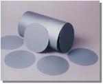
4 Wafer Processing Silicon single crystal growth from polysilicon Silicon ingot with impurities is created Ingot diameter can vary from 100mm to 300mm Wafers are sliced from the ingot Typically µm m thick
5 Wafer Processing
6 Wafer Processing
7 Wafer Processing Why the trend to larger wafers? More chips per wafer Less waste After slicing Lapping Polishing Defect detection
8 Semiconductor Processing Oxide Layer - SiO 2 (sand) Heat Wafer in an oxidizing atmosphere - water vapor or pure oxygen gas Oxide P-Type Silicon Wafer
9 Semiconductor Processing How do you control where the features get placed? Photolithography masks Oxide P-Type Silicon Wafer
10 Semiconductor Processing Need to remove the oxide layer Photoresist Oxide P-Type Silicon Wafer
11 Semiconductor Processing Need to remove the oxide layer UV Light Mask Photoresist Oxide P-Type Silicon Wafer
12 Semiconductor Processing Need to remove the oxide layer Acid Etching Photoresist Oxide P-Type Silicon Wafer
13 Semiconductor Processing Add polysilicon layer for gate Mask Oxide P-Type Silicon Wafer
14 Semiconductor Processing Impurity injection Diffusion Wafers are placed in a heated tube with dopant gas At high temperatures (~1000ºC), the dopant diffuses into the exposed regions of the wafer Ion Implantation Dopants are introduced as ions into material by sweeping a beam across the material Depth of implantation and density is controlled by the acceleration and exposure time High energy implantation can cause lattice damage Deposition Deposit a gas or vapor (CVD) on the wafer at high temperatures
15 Semiconductor Processing Impurity injection Ion implantation Mask Oxide P-Type Silicon Wafer
16 Semiconductor Processing Add Oxide insulation layer Oxide P-Type Silicon Wafer
17 Semiconductor Processing Add Metal layer Oxide
18 Semiconductor Processing pmos Transistor Oxide n Well P-Type Silicon Wafer
19 Interconnect Polysilicon to Metal contacts Diffusion to Metal contacts Diffusion to Polysilicon silicide contacts Metal to Metal vias
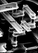
20 Metallization
21 Packaging Requirements Electrical: Low parasitics Mechanical: Reliable and robust Thermal: Efficient heat removal Economical: Cheap
22 Bonding Techniques Wire Bonding Substrate Die Pad Lead Frame
23 Tape-Automated Bonding (TAB) Sprocket hole Film + Pattern Solder Bump Test pads Die Lead frame Substrate (b) Die attachment using solder bumps. (a) Polymer Tape with imprinted wiring pattern. Polymer film
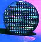
24 Flip-Chip Bonding Die Solder bumps Interconnect layers Substrate
25 Package-to-Board Interconnect (a) Through-Hole Mounting (b) Surface Mount

26 Package Types
27 Package Parameters
28 Trends in Process Technology Copper Conductors Silicon on Insulator Strained Silicon Three-dimensional ICs
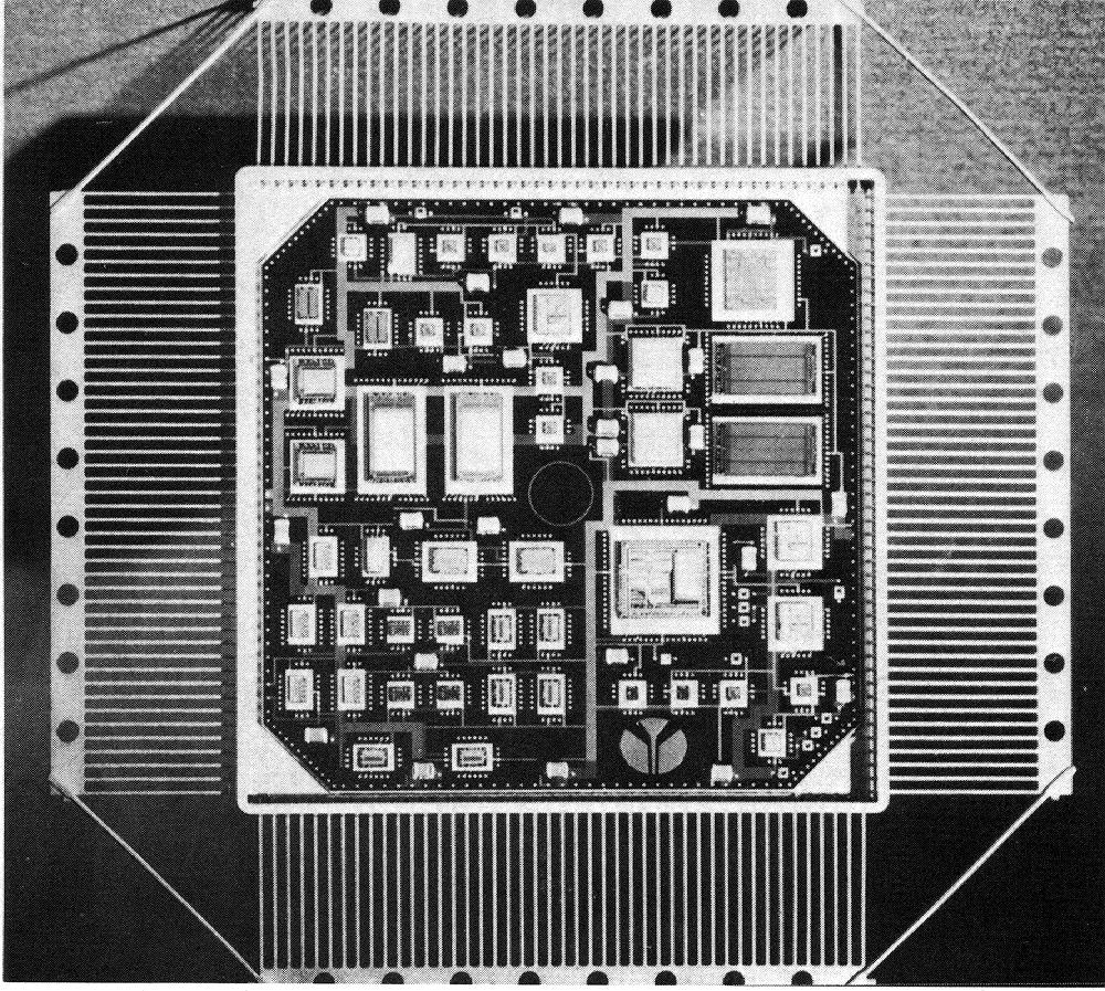
29 Multi-Chip Modules
30 CMOS Process Layers Layer Well (p,n) Active Area (n+,p+) Select (p+,n+) Polysilicon Metal1 Metal2 Contact To Poly Contact To Diffusion Via Color Yellow Green Green Red Blue Magenta Black Black Black Representation

31 Layers in 0.25 µm m CMOS process
32 Semiconductor Masks n+ diffusion
33 Semiconductor Masks n+ polysilicon
34 Semiconductor Masks n+ polysilicon contact
35 Semiconductor Masks n+ metal polysilicon contact
36 Semiconductor Masks p+ metal polysilicon contact
37 Semiconductor Masks VDD VIN VOUT VSS
38 Design rules Design rules are critical to proper operation of the circuit They place restrictions on the sizes of layers and the distance between layers Often expressed in terms of λ - half the minimum feature size

39 Design Rules MOSIS SCMOS Design Rules Contact size Minimum poly overlap Minimum contact spacing Minimum spacing to gate of transistor 2x
40 CMOS Latchup
41 CMOS Latchup
42 CMOS Latchup pmos p+ Source n well substrate R well Acts like a SCR (silicon controlled rectifier) As long as both transistors are off, everything is fine R substrate nmos n+ Source
43 CMOS Latchup pmos p+ Source n well substrate I well R well External disturbance causes current flow in R sub or R well Feedback loop will cause the current draw to increase dramatically R substrate nmos n+ Source
44 CMOS Latchup External disturbances ESD (electrostatic discharge) stress Cosmic rays/alpha particles Sudden transients on Vdd or Gnd I/O pads interfacing with large currents off chip
45 CMOS Latchup Avoiding latchup Decrease R sub and R well so that it is harder to turn on the BJT transistors Place substrate and well contacts close together Keep pmos transistors close to Vdd and nmos transistors close to ground Surround transistors in I/O pads with guard rings Decrease β of BJT transistors Space the pmos and nmos transistors apart
46 Next Class Performance Characterization Read Chapter 4