Control of nickel silicide formation using porous silicon in direct plating concepts for silicon solar cell front side metallization
|
|
|
- Melina Janel Melton
- 5 years ago
- Views:
Transcription

1 Control of nickel silicide formation using porous silicon in direct plating concepts for silicon solar cell front side metallization 3rd Workshop on Metallization for Crystalline Silicon Solar Cells Charleroi, Belgium, 25-26th October 2011 Dr. Dietmar Lütke Notarp
2 Outline Motivation Challenges Crucial elements and benefits of presented Direct Plating approach Process flow details Electrical results Summary / Conclusion / Outlook 2
 Reduction of line resistance at same or less metal volume / line width (no porous metal lines from printed")

3 Motivation for Direct Plating on Silicon Increase of cell efficiency Improved contact resistance (Ni-Si contact possible) Reduction of line resistance at same or less metal volume / line width (no porous metal lines from printed pastes involved) Cost reduction: Replacement of silver (silver price) Silver plating on silver paste? Silver plating on silicon? -> Intermediate step, but no match to the benefits of direct plating Ag direct on silcon Ni Cu Sn direct on silcon 3


 Adhesion of plated metals (during process and")

4 Challenges Technical Nitride opening method? Nitride residues? Nitride protection needed or compatibility provided? Backside compatibility (Al in wet chemistry?!) Adhesion of plated metals (during process and finished stack) Depth control of silicide formation / shunting Overall complexity of process flow Commercial CoO need to be less than 16Eurocents to be competetive with Ag on Ag 4
 Multiple functions of the printed resist: Etching mask during nitride etch and porous silicon anodisation")
 -> plating INTO the pores Plating with dry backside -> compatible to all")
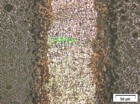
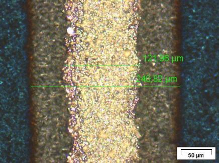
5 Crucial elements of the approach Porous silicon: control of Ni-silicide formation -> Ni-silicide is limited to porous silicon layer HF-resistant screen-printable etch mask (Maramask PV-HF) Multiple functions of the printed resist: Etching mask during nitride etch and porous silicon anodisation Plating mould (reduced lateral growth) Nitride protection (low-quality nitride can be processed) Resist removal without solvants Porosification and plating of Ni from single bath (switch the current from anodic to cathodic) -> plating INTO the pores Plating with dry backside -> compatible to all media suncup tool 5
6 Benefits of the concept Silicide formation at C AFTER completion of plated stack no wet-dry-wet cycle for intermediate silicide formation needed Good adhesion as plated at all times (plating of full stack before silicide formation) No selective emitter needed shallow silicide less than 50nm deep No limitation for contacting of 100Ohm emitter (or higher) CoO ~ 8Eurocents per wafer Minor impact on production line existing lines can be upgraded change silver printer to resist printer Wet chemistry tooling (etching, plating, resist removal) Additional oven for silicide formation 6


7 Direct plating on silicon process flow 7


8 Electrical results Result of a conventional industrial processed mc-si solar cell with direct plating contacts on the front side. DLIT measurement at 0.6 mv forward bias No shunting EL measurement at 1.5 A forward bias Contact formation on the whole cell area. 8
9 Summary / Conclusion / Outlook The feasibility of using porous silicon for the control of the Ni- Silicide formation depth was demonstrated A production-fit process flow for upgrading existing lines was presented. Screen printing of resist needs to be introduced, still the impact on the production line is low. Direct plating on silicon is a logical step for future front side metallisation concepts Process flow can be evaluated/verified using NBT s suncup wet chemistry tool Industrial tools for the presented concept are under construction. Targets to launch a tool and process in 2012/13 9


10 Thank you for your attention Acknowledgements Marabu GmbH Dr. Dietmar Lütke Notarp NB Technologies GmbH Hans Frintrup GmbH Fahrenheitstr Bremen RWTH Aachen IHT - Institute of Semiconductor Electronics 10 Ludwig-Erhard-Allee Bonn info@nb-technologies.de Dr. D. Lütke Notarp