Title. Author(s)Kikuchi, T.; Takahashi, H.; Maruko, T. CitationElectrochimica Acta, 52(7): Issue Date Doc URL.
|
|
|
- Hugh Greer
- 5 years ago
- Views:
Transcription
1 Title Fabrication of Three-Dimensional Platinum Microstruc Author(s)Kikuchi, T.; Takahashi, H.; Maruko, T. CitationElectrochimica Acta, 52(7): Issue Date Doc URL Type article (author version) File Information kikuchi2.pdf Instructions for use Hokkaido University Collection of Scholarly and Aca
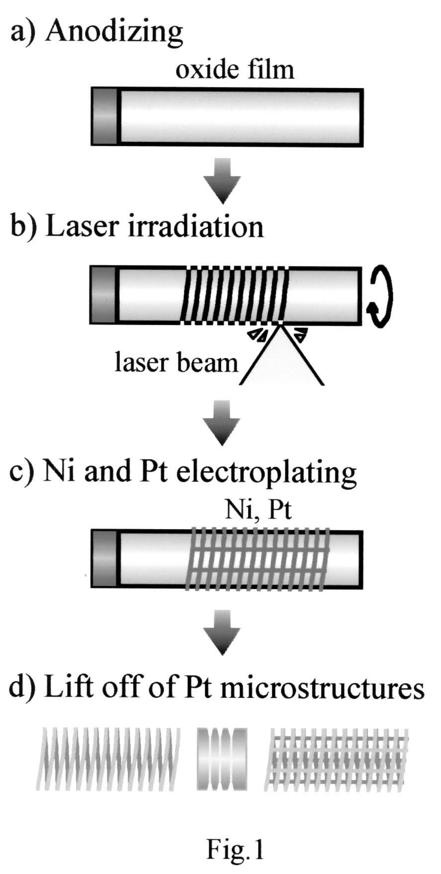
2 Fabrication of Three-Dimensional Platinum Microstructures with Laser Irradiation and Electrochemical Technique T. Kikuchi a, *, H. Takahashi a, and T. Maruko b a Graduate School of Engineering, Hokkaido University, N13, W8, Kita-Ku, Sapporo, Japan b Furuya Metal Co. Ltd., R&D Group, Shimodate Daiichi Kogyodanchi 1915, Morisoejima, chikusei, Ibaraki, Japan Corresponding author: T. Kikuchi TEL: FAX: kiku@elechem1-mc.eng.hokudai.ac.jp Abstract Three-dimensional platinum microstructures were fabricated by successive procedures: aluminum anodizing, laser irradiation, nickel / platinum electroplating, and removal of the aluminum substrate, the oxide films, and the nickel metal layer. Aluminum plates and rods were anodized in an oxalic acid solution to form porous type 1
3 oxide films. The anodized specimens were immersed in a nickel electroplating solution, and then irradiated with a pulsed Nd-yttrium aluminum garnet (YAG) laser beam to remove the anodic oxide film with a three-dimensional XYZθ stage. The specimens were cathodically polarized in the nickel and a platinum electroplating solution to form the metal micropattern at the laser-irradiated area. The electroplated specimens were immersed in NaOH solution to dissolve the aluminum substrate and the oxide films, and then immersed in HCl solution to dissolve the nickel deposits. A platinum grid-shaped microstructure, a microspring, and a cylindrical network microstructure with µm line width were obtained successfully. Key words: Aluminum, Platinum, Laser Irradiation, Electroplating, MEMS 1. INTRODUCTION Platinum group metals (PGM) have been widely used in many industries due to its chemical stability, high temperature resistance, and catalytic reactivity [1-5]. Especially the platinum metal with high chemical stability has been investigated to 2
4 fabricate microstructure such as microelectromechanical systems (MEMS) and micro-bio-devices. Haro et al. worked on fabrication of implantable microelectrode arrays using selective platinum coating, and obtained the microelectrode with good adhesive and high corrosion resistance [6]. Kashimura et al. fabricated electrodes with sub-10-nm gap using electron beam lithography and conventional electroplating technique, and this structure will be used for physical measurements of single molecules or nanoparticles [7]. Micropatterning of platinum electrode on silicon substrate for MEMS was achieved by Zaborowski et al. using wet etching process with photolithography [8]. Recently more complicated microstructure of platinum is needed in application for MEMS, but photolithography is seldom applied to fabrication of three-dimensional (3D) microstructures. The authors have been developing a new method for 3D microstructure fabrication of metals and organic compounds using laser irradiation and electrochemical technique [9-15]. In this technique, an aluminum specimen covered with porous type oxide films was irradiated with a pulsed Nd-yttrium aluminum garnet (YAG) laser in a solution to remove the oxide film. Then, electroplating was carried out for the formation 3
5 of metal or organic compound micropattern at the laser-irradiated area, and the microstructure could be obtained by lifting off process. Three-dimensional nickel microstructures, such as microspring, 3D network micostructure, microring, and microbellows were fabricated by the processes described above [9]. A microactuator with nitrocellulose / nickel / polypyrrole three-layer structure was also obtained by electrolytic polymerization of conducting polymer [11]. In the present investigation, the authors fabricated 3D platinum microstructures by aluminum anodizing, laser irradiation, electroplating, and lifting off. 2. EXPERIMENTAL 2.1 Specimens and pretreatment Highly pure aluminum plate (99.99 wt%, 0.35 mm thick, 20 x 18 mm with a handle, Nippon Light Metal) and commercial aluminum tube (99.5 wt%, 1.6 mm i.d., 2.0 mm o.d., 35 mm long, Nilaco) were used as the specimens. These specimens were degreased ultrasonically in C 2 H 5 OH for 10 min, and then electropolished in 13.6 M CH 3 COOH / 2.56 M HClO 4 solution at 28 V and 280 K. After electropolishing, the 4
6 specimens were anodized in 0.22 M (COOH) 2 solution at 293 K for 30 min with a constant current of 100 A/m 2 to form 9 µm thick porous type oxide films. The anodized specimens were immersed in M alizarin red S dying solution at 323 K for 5 min, and then boiled in doubly distilled water for t s = min to seal the pores. 2.2 Immersion test of anodized specimen in platinum electroplating solution The anodized specimens were immersed in a platinum electroplating solution (ph = 9.0) for 120 min whose chemical composition is shown in Table 1. Structural changes of specimens after immersion were examined by confocal scanning laser microscopy (CSLM: 1SA21, LASERTEC). 2.3 Fabrication of platinum microstructures The anodized specimens were immersed in doubly distilled water or 0.31 M NiSO 4 / 0.40 M H 3 BO 3 solution (nickel electroplating solution) at 293 K, and then irradiated with a Pulsed Nd-YAG laser. The specimens were set in a focal position or a defocused position 5 mm from the focal plane of the laser beam that had passed through a beam splitter, an iris diaphragm, a convex lens with 60 mm focal length, and a quartz 5
7 window. The laser beam has 532 nm wavelength, 8 ns pulse width, 10 Hz frequency, and < 0.5 mrad beam divergence (full angle). Details of the laser irradiation setup have been shown elsewhere [11]. During the laser irradiation, the specimens were moved at 80 µm/s with a PC-controlled XYZ-stage, and rotated at degree/s with a θ stage to remove the oxide film continuously from the aluminum substrate. The laser-irradiated specimens were cathodically polarized in the nickel electroplating solution for 1 min at constant potential of -1.2 V (vs. saturated KCl-Ag/AgCl) and 293 K. A platinum plate was used as the counter electrode for the electroplating. After laser irradiation and nickel electroplating, the specimens were immersed in platinum electroplating solution, and then cathodically polarized for min at constant current density of A/m 2 and 353 K to form the platinum micropatterns. Some specimens were subjected to platinum electroplating without nickel plating to examine the role of nickel deposits in the subsequent platinum plating. Finally, platinum-electroplated specimens were immersed in 3 M NaOH solution at room temperature for about 2 hr to dissolve the aluminum substrate and the anodic oxide films, and then were immersed in 12 M HCl solution at room temperature for 5 6
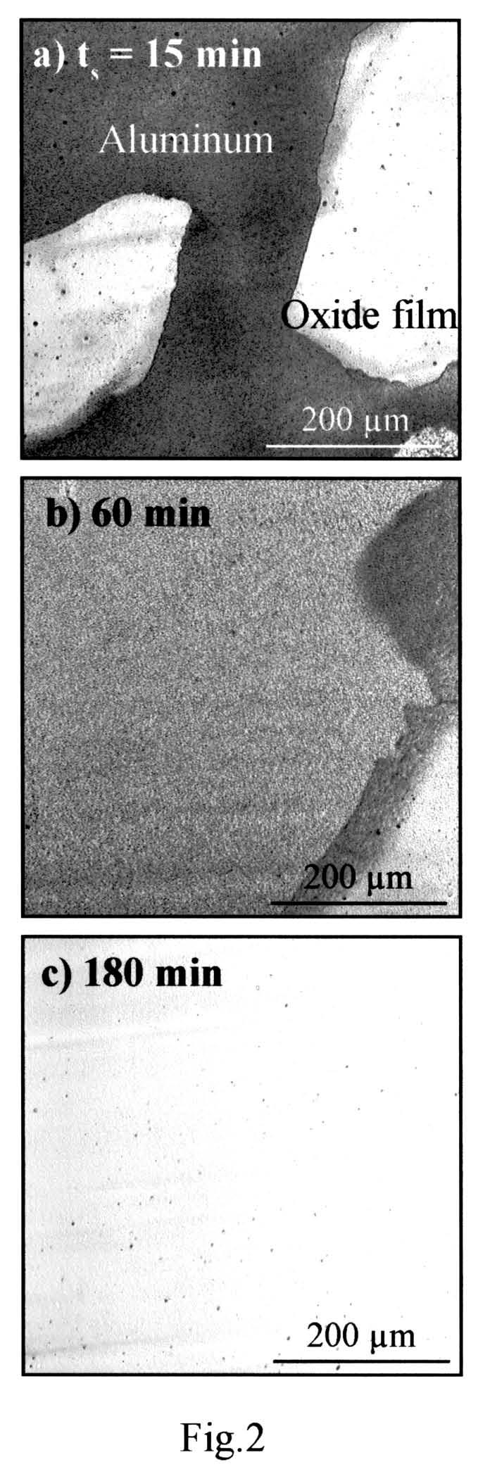
8 min to dissolve the nickel deposits. The fabrication process of the three-dimensional platinum microstructures is shown in Fig. 1. Structural changes of the specimen by laser irradiation, electroplating, and lifting off were examined by CSLM and field emission scanning electron microscopy (FESEM: JSM-6300F, JEOL). In the observation of the vertical cross section of specimens, the specimens were embedded in epoxy resin and polished mechanically. 3. RESULTS AND DISCUSSION 3.1 Effect of pore-sealing on film dissolution in platinum electroplating solution Fig. 2 shows CSLM two-dimensional (2D) contrast images of the surface of anodized aluminum specimens with different pore-sealing times of a) t s = 15, b) t s = 60, and c) t s = 180 min after immersion in platinum electroplating solution for 120 min. It is clear that there are white and gray parts in t s = 15 min (Fig. 2a) and 60 min (Fig. 2b). These white parts correspond to anodic oxide films and the gray parts to aluminum substrate. The aluminum substrate with rough surface can be observed here due to dissolution of the anodic oxide films in platinum electroplating solution with high ph. 7
9 However, at t s = 180 min (Fig. 2c), there is no dissolved area of the oxide films. Pore-sealing in boiling water causes the hydration of oxide to seal the pores in the oxide films by the volume expansion [16] Al 2 O 3 + nh 2 O = Al 2 O 3 nh 2 O (1) The imperfections in the anodic oxide films decrease by the volume expansion of the oxide films. In addition, a highly crystalline hydroxide layer is formed on the surface of the oxide films, and the hydroxide layer is highly dissolution-resistant in acid and alkaline solutions [17]. Thickness and the crystallinity of the hydrated oxide layer increase with pore-sealing time, t a, resulting in a high stability of the anodic oxide films in platinum electroplating solution. The anodic oxide films after sealing for t s = 180 min remained undissolved in platinum electroplating solution until 240 min. 3.2 Effect of electroplating conditions on the fabrication of platinum micropattern Fig. 3 shows the cathodic polarization curve, cathodic current density, i a, versus cathodic potential, E c, in platinum electroplating solution at 353 K on a platinum plate. The i c value increases as E c becomes higher between -100 to -200 mv, and then steady value of about 1 A/m 2 until E c = -550 mv, followed by a linear increase with E c. The 8
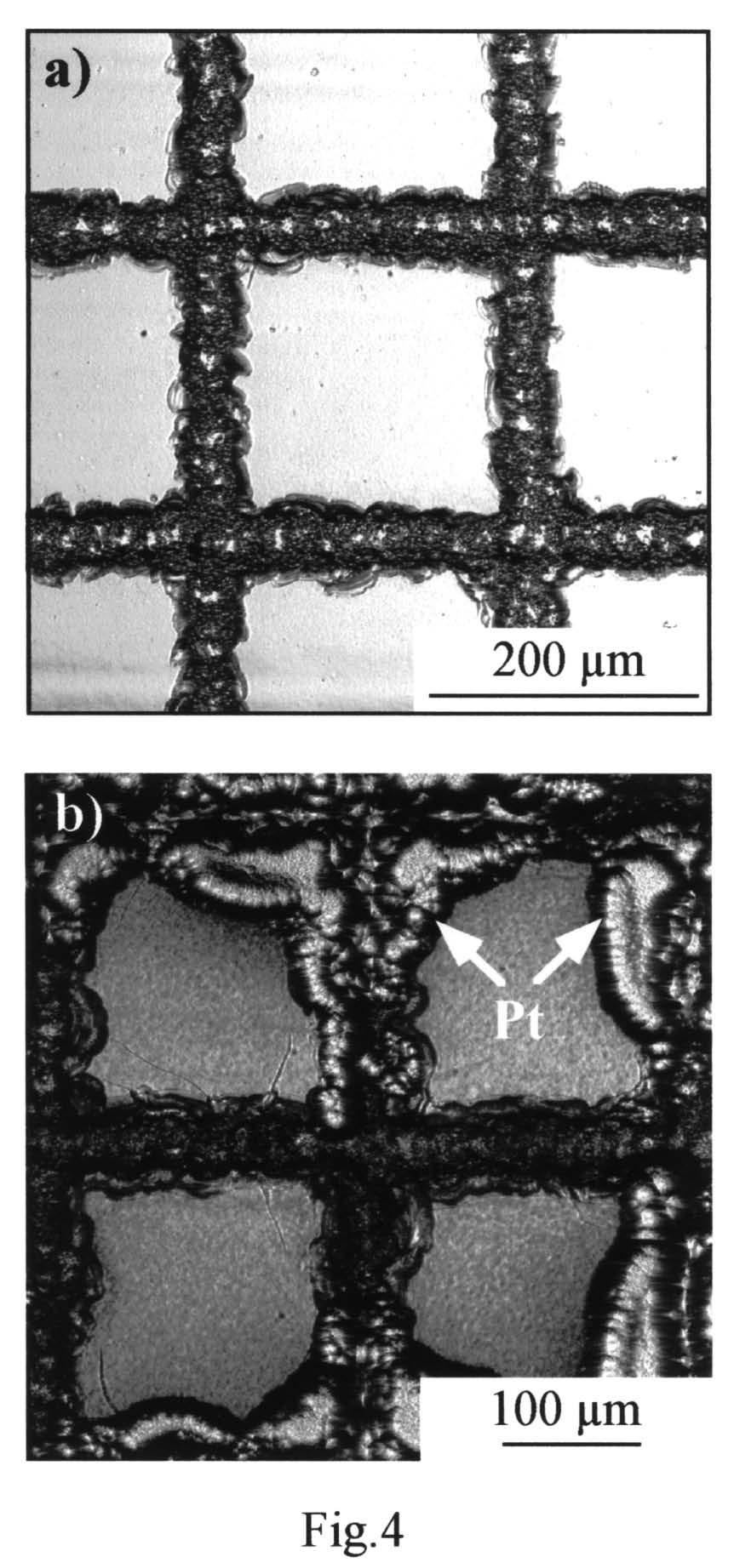
10 steady value of i c at -200 to -550mV corresponds to diffusion-limited reduction of dissolved oxygen in electroplating solution, while increase in i c above E c = -550 mv corresponds to electrodeposition of platinum metal and hydrogen evolution. Fig. 4a shows a CSLM contrast image of the surface of the specimen irradiated with the laser at P = 1.0 mw in doubly distilled water to form a grid pattern. The black lines correspond to the laser-irradiated area, and the white background to the anodic oxide films that was not laser irradiated. It is clear that the anodic oxide films are removed continuously with about 50 µm line width. The periodic changes of the film-removed line width are due to the scanning of the laser beam with circle shape. Three-dimensional height images of the CSLM and the vertical cross-section of the specimen showed that the oxide film was completely removed by laser irradiation, and the aluminum substrate is exposed to water at laser-irradiated area. Fig. 4b shows a CSLM image of the surface of the specimen with platinum electroplating at i c = 150 A/m 2 for electroplating time, t c = 180 min after laser irradiation in distilled water. Electrodeposited platinum can be observed on all the laser-irradiated areas except for the center region of the image. There are concaves at the center region, suggesting no 9
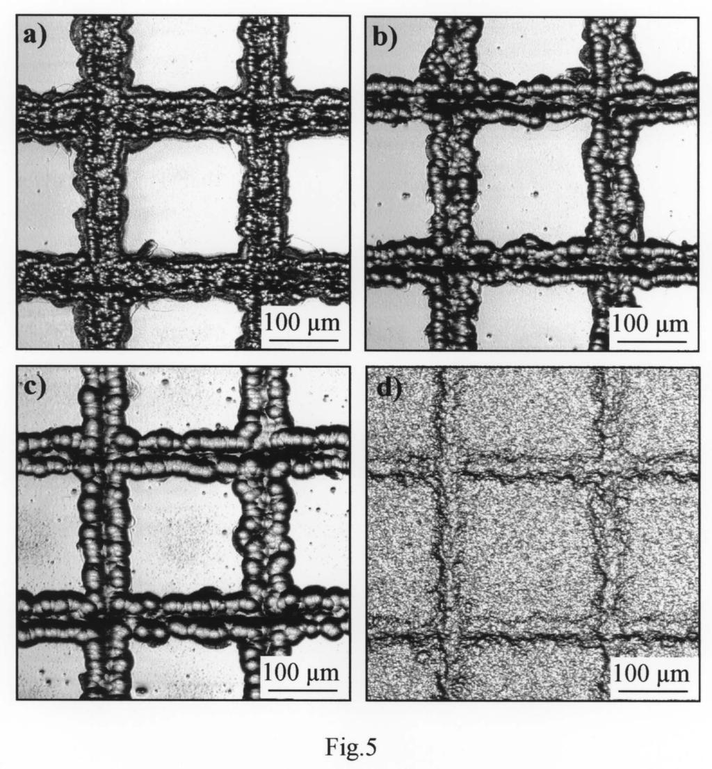
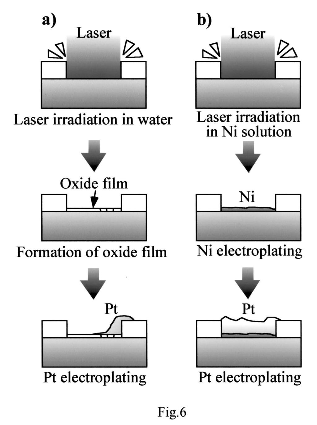
11 platinum deposition. The deposited platinum is on the oxide films around the laser-irradiated area as well as on the film-removed area. This overflow of platinum is due to the spread of platinum onto the anodic oxide film from the laser-irradiated area. Platinum micro-patterning with continuous metal lines could not be obtained by the direct platinum electroplating under conditions with different t c s and i c s. Fig. 5 shows CSLM images of the surface of the specimen after platinum electroplating at current density, i c = a) 50, b) 100, c) 150, and d) 200 A/m 2 and 353 K for 180 min. Here, the specimens were irradiated with the laser in the nickel electroplating solution, and then cathodically polarized to deposit nickel at the laser-irradiated area before platinum electroplating. The continuous platinum lines can be observed at the laser-irradiated areas at i c = A/m 2 (Figs. 5a-c), and the line width is µm, showing wider lines at higher i c. Platinum deposits are composed of dome-shaped grains and the grain size is lager at higher i c. At i c = 200 A/m 2 (Fig. 5d), all the surface is covered with platinum metal with small particles, i. e. platinum metal is deposited at non laser-irradiated areas as well as laser-irradiated areas. Observation of the vertical cross-section of the specimen 10
12 showed that anodic oxide films were completely removed after platinum electroplating at i c = 200 A/m 2. The effect of nickel plating on the deposition behavior of platinum is discussed bellow. The non-uniform platinum electrodeposition in the case of laser irradiation in distilled water (Fig. 4b) is considered to be due to the formation of thin hydroxide film at the laser-irradiated area after laser irradiation (Fig. 6a). The oxide films may have fine imperfections locally. Platinum may be deposited through these imperfections, leading to the non-uniform deposition of platinum On the other hand, the laser irradiation in Ni 2+ ion containing solution and the subsequent nickel electroplating suppress the formation of hydroxide film at the film-removed area. This is due to the chemical deposition of nickel nano-particles during laser irradiation and nickel thin layer formation during short electroplating (Fig. 6b). Therefore, the nickel thin layer may also suppress the dissolution of anodic oxide film and aluminum substrate during platinum electroplating, resulting in the deposition of platinum continuous lines whose width is very similar to that of film removed area (Figs. 5a - c). The reason why whole surface of the aluminum specimen is covered with platinum metal layer at high current density is discussed bellow. The current efficiency for 11
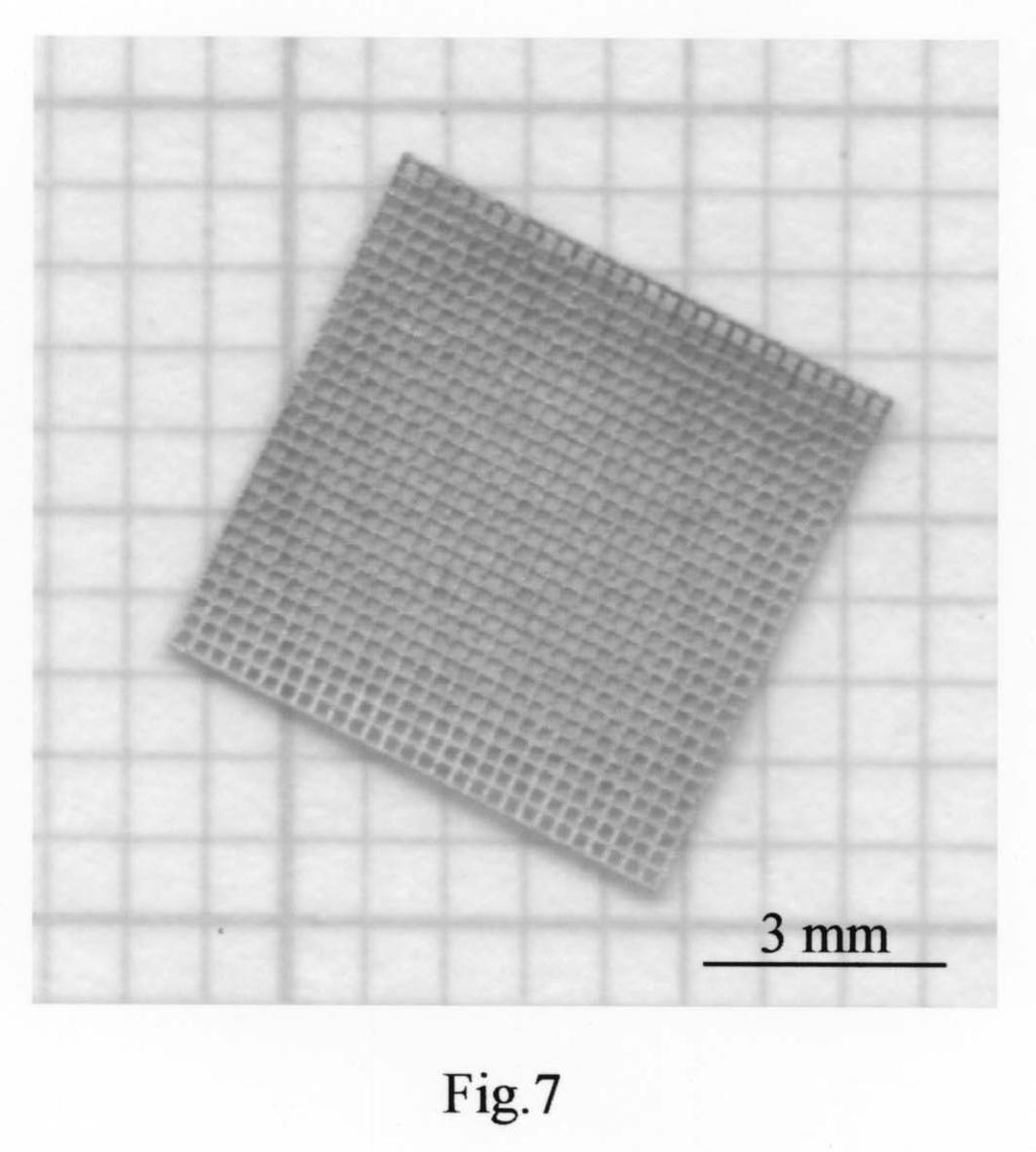
13 platinum deposition under the electroplating conditions in this investigation is % [16], and platinum deposition is associated with hydrogen evolution, which occurs at the interface between oxide films and the metal substrate by penetration of proton through imperfections of the oxide films. At higher on current densities, hydrogen evolution is more vigorous, and may cause the removal of the oxide films from the aluminum substrate leading to the platinum deposition on the whole surface of aluminum substrate (Fig. 5d). 3.3 Fabrication of 3D platinum microstructures Fig. 7 shows an optical micrograph of platinum grid-shaped microstructure that was obtained by anodizing, laser irradiation, nickel / platinum electroplating, and aluminum substrate / oxide films / nickel dissolution. It is clear from Fig. 7 that free-standing platinum micro-grid can be obtained by the successive procedures described above. The platinum metal has 50 µm line width, 190 µm gap intervals, and 10 µm thick. The deformation of platinum microstructure by removal of the aluminum, the oxide films, and nickel metal layer cannot be observed, and the line intervals of the microstructure are extremely regular. 12
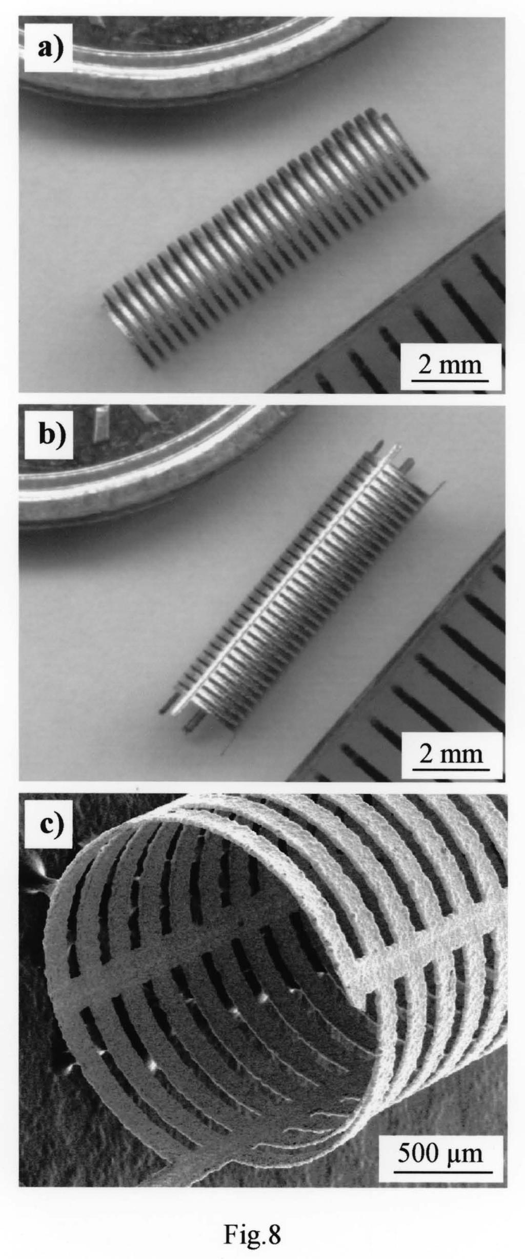
14 Figs. 8a and 8b show CSLM image of 3D platinum microstructures fabricated by the process shown in Fig. 1 with commercial aluminum tube. A platinum microspring with 2 mm spring diameter and 110 µm metal line width is shown in Fig 8a. The pitch of coil of the microspring appears to be very uniform, while the diameter to be slightly fluctuated. Fig. 8b shows a cylindrical platinum network microstructure with 2 mm diameter and 110 µm metal line width. This microstructure consists of microspring described above, connected by 4 pillars, and the line intervals of the microstructure are regular because the pillars prevent deformation during immersion of NaOH and HCl solutions. Fig. 8c shows high magnification FESEM image of the cylindrical platinum network microstructure. The microstructure is composed of small platinum grain, and the thickness of platinum layer is about 15 µm. The 3D platinum microstructures obtained in the present investigation are difficult to be fabricated by photolithography since a flat photo-mask may cause a distortion of the 3D structure. The technique described here can be applied to fabricate 3D structures with carved surface, pyramids, spheres, cones as well as cylinders. The platinum 3D microstructures are able to be used in the field of electrochemical industry, 13
15 MEMS, micrototal analysis systems (µtas) and micro-bio-devices. 4. CONCLUSIONS The following conclusions may be drawn. (1) The anodic oxide films on the aluminum specimen after pore sealing in distilled water for 180 min have good insulating properties in platinum electroplating solution. (2) Non-uniform platinum electrodeposition occurs on the laser-irradiated area in platinum electroplating after laser irradiation in distilled water, while uniform platinum micropatterning can be achieved by electroplating after formation of thin nickel metal layer on the aluminum substrate. (3) A combination of the procedures of aluminum anodizing, laser irradiation, nickel / platinum electroplating, and aluminum substrate, oxide films, and nickel metal layer dissolution enables fabrication of three-dimensional platinum microstructures such as grid, microspring, and cylindrical network. References 14
16 1) C. R. K. Rao and D. C. Trivedi, Coord. Chem. Rev. 249 (2005) 613 2) R. Burch, J. P. Breen, and F. C. Meunier, Appl. Catal. B 39 (2002) 283 3) Z. M. Rdzawski and J. P. Stobrawa, J. Mater. Process. Technol (2004) 681 4) T. Matsui, K. Fujiwara, T. Okanishi, R. Kikuchi, T. Takeguchi, and K. Eguchi, J. Power Sources 155 (2006) 152 5) J. Garcia, H. T. Gomes, P. Serp, P. Kalck, J. L. Figueiredo, and J. L. Faria, Catal. Today (2005) 101 6) C. de Haro, R. Mas, G. Abadal, J. Munoz, F. Perez-Murano, and C. Dominguez, Biomaterials 23 (2002) ) Y. Kashimura, H. Nakashima, K. Furukawa, and K. Torimitsu, Thin solid Films (2003) 317 8) M. Zaborowski, P. Grabiec, and A. Barcz, Microelectron. Eng. 82 (2005) 283 9) T. Kikuchi, M. Sakairi, H. Talahashi, Y. Abe, and N. Katayama, J. Electrochem. Soc. 148 (2001) C740 10) T. Kikuchi, M. Sakairi, H. Talahashi, Y. Abe, and N. Katayama, Surf. Coat. Technol. 169 (2003)
17 11) T. Kikuchi, M. Sakairi, and H. Takahashi, J. Electrochem. Soc. 150 (2003) C567 12) T. Kikuchi, S. Z. Chu, S. Jonishi, M. Sakairi, and H. Takahashi, Electrochim. Acta 47 (2001) ) Y. Akiyama, T. Kikuchi, M. Ueda, M. Iida, M. Sakairi, and H. Takahashi, Electrochim. Acta in press (Elsevier, Science Direct) 14) T. Kikuchi, H. Takahashi, and T. Maruko, J. Surf. Finish. Soc. Jpn. 56 (2005) ) T. Kikuchi and H. Takahashi, J. Surf. Finish. Soc. Jpn. 56 (2005) ) N, Masuko, Hyoumen-Gijutsu Binran, Nikkan Kogyo Shimbun, Tokyo, 1998, 273, 549 pp. 17) M. Koda, H. Takahashi, and S. Nagayama, J. Surf. Finish. Soc. Jpn. 33 (1982)
18 Captions Table. 1 Composition of platinum electroplating solution. Fig. 1 Fabrication of three-dimensional platinum microstructures by anodizing, laser irradiation, nickel / platinum electroplating, and dissolution of aluminum substrate / oxide films / nickel deposits. Fig. 2 CSLM images of the surface of the specimen pore-sealed for a) t s = 15 min, b) 60 min, and c) 180 min after immersion in platinum electroplating solution for 120 min. Fig. 3 Change in cathodic current density, i c, with cathodic potential, E c, in platinum electroplating solution using platinum plate. Fig. 4 CSLM images of the surface of the specimen after a) laser irradiation in distilled water and b) platinum electroplating. Fig. 5 CSLM image of the surface of the specimen after laser irradiation in nickel electroplating solution, nickel electroplating, and platinum electroplating. The current densities of platinum electroplating, i a, are a) 50, b) 100, c) 150, and d) 200 A/m 2. Fig. 6 Schematic models of a) non-uniform platinum deposition and b) uniform platinum deposition. 17
19 Fig. 7 Optical micrograph of the platinum mesh-like microstructure fabricated by anodizing of aluminum plate, laser irradiation, nickel / platinum electroplating, and aluminum substrate / oxide film / nickel metal dissolving. Fig. 8 CSLM and FESEM images of the 3D platinum microstructures; a) microspring and b) - c) cylindrical network microstructure. 18
20 Chemicals Concentration / M Pt(NH 3 ) 2 (NO 2 ) CH 3 COONa 0.85 Na 2 CO CH 3 COOH for ph adjustment 19
21
22
23
24
25
26
27
28