Developments in Quantitative EDS Analysis, with a Focus on Light Element and Low Energy Peaks. Webinar 2 June 2010
|
|
|
- Darren Lawrence
- 5 years ago
- Views:
Transcription


1 Developments in Quantitative EDS Analysis, with a Focus on Light Element and Low Energy Peaks Webinar 2 June 2010


2 Panelists Orkun Tunçkan, Cand. PhD., Materials Science and Engineering Department, lecturer at the School of Civil Aviation, Anadolu University, Eskişehir, Turkey Dr. Tobias Salge, Application Scientist, Bruker Nano GmbH, Berlin, Germany Dr. Ralf Terborg, Methodology Specialist, Bruker Nano GmbH, Berlin
3 Content Quantification using Esprit Optimizing quantification methods using the method editor Examples: Steel Light element and low energy quantification From micro to nano, EDS analysis at the nanoscale Examples: Ceramics, semiconductor, solar cells, minerals Orkun Tunckan: Ceramic metal joints
4 Details: From micro to nano 1. Standardless analysis with kv 2. Standardless analysis at the nanoscale with 4 15 kv 3. Standard-based analysis at the nanoscale with kv

5 Quantification steps Ident BG Deconv Quant
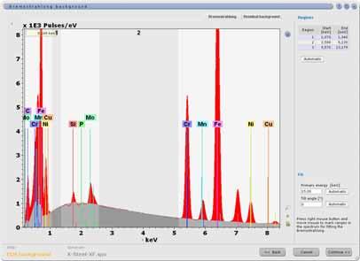
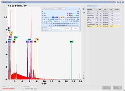
6 Quantitative analysis steps 1. Identification: Comparison between the peaks found in the spectrum and the atomic data (line energies and intensities) 2. Background: Calculation of the physical Bremsstrahlung background based on the assumed sample composition or mathematical filter 3. Deconvolution: The BG corrected peak intensities, especially at line overlaps, are attributed to the element lines 4. Quantification: Element concentrations are calculated from deconvolved line intensities: standardless P/B-ZAF and PhiRhoZ, standardbased PhiRhoZ


7 Method editor
8 Microanalysis 1) Standardless microanalysis with kv Round robin test of Cr-Ni-steel Discrimination of molybdenum and sulfur by peak deconvolution Quantification of elements near the detection limit Comparison of EDS quantification with WDS and ICP-OES results
9 Qualification and quantification Cr-Ni-steel Interlaboratory test EDS 2009 nanoanalytics 2 samples: Chromium-Nickel-steel (1.4310, ) Comments nanoanalytics Bruker standardless (P/B-ZAF) und standard-based (PhiRhoZ) quantification result compared to WDS and ICP-OES

10 Comments nanoanalytics Manganese/ Chromium: There is an overlap between the manganese peak and the much higher chromium. Thus, it was more difficult for the participants to detect about 1 wt% of manganese than 0.6 wt% silicon.


11 Solution: Deconvolution Bad match => Missing element Perfect match => Correct identification

12 Comments nanoanalytics Sulfur/ Molybdenum : Obviously, the EDS systems / participants prefer to choose either molybdenum or sulfur... "
13 Distinguishing molybdenum and sulfur Mo only 80 x 0,001 cps/ev S only 80 x 0,001 cps/ev Mo + S 80 x 0,001 cps/ev Mo S Mo S kev Mo: 0.29 wt.% Perfect match! kev S: 0.13 wt.% Bad match! kev Mo: 0.26 wt.% S: 0.01 wt.% Sulfur concentration below detection limit!
14 A closer look 300 x 0,001 cps/ev V Cr Mn Fe Co Ni Cu kev Additional identification of vanadium, cobalt and copper!
15 Preset method with one click Quantification steps can be saved to a preset method.


16 Preset method with one click Quantification steps can be saved to a preset method. This preset method can be used to analyze a large number of similar samples automatically.


17 Detection limit of EDS
18 Interlaboratory test: Cr-Ni-steel Quantax results compared to ICP-OES and WDS Standardless P/B-ZAF and standard-based PhiRhoZ quantification Sample (n=4) Sample (n=4) Method Stdless 1 Std 2 ICP-OES WDS Stdless 1 Std 2 ICP-OES WDS Si V <0.08 < Cr Mn Fe Co Ni Cu Mo Total : Cobalt was quantified with reference. 2 : Vanadium was quantified standardless. Elements near the detection limit are in good agreement with WDS and ICP analysis.
19 Interlaboratory test: Cr-Ni-steel QUANTAX results compared to ICP-OES and WDS Standardless P/B-ZAF and standard-based PhiRhoZ quantification Sample (n=4) Sample (n=4) Method Stdless 1 Std 2 ICP-OES WDS Stdless 1 Std 2 ICP-OES WDS Si V <0.08 < Cr Mn Fe Co Ni Cu Mo Total : Cobalt was quantified with reference. 2 : Vanadium was quantified standardless. Elements near the detection limit are in good agreement with WDS and ICP analysis.
20 Interlaboratory test: Cr-Ni-steel QUANTAX results compared to ICP-OES and WDS Standardless P/B-ZAF and standard-based PhiRhoZ quantification Sample (n=4) Sample (n=4) Method Stdless 1 Std 2 ICP-OES WDS Stdless 1 Std 2 ICP-OES WDS Si V <0.08 < Cr Mn Fe Co Ni Cu Mo Total : Cobalt was quantified with reference. 2 : Vanadium was quantified standardless. Elements near the detection limit are in good agreement with WDS and ICP analysis.
 Si, 20 kv Si, 10 kv Si, 5 kv ~4000 nm ~1500 nm")
21 Nanoscopic EDS analysis Monte Carlo simulation of electron trajectories for Si for different accelerating voltages (primary beam diameter ~1 nm) Si, 20 kv Si, 10 kv Si, 5 kv ~4000 nm ~1500 nm ~400 nm
 and transition metals up to Zn (Z=30), e.g.")
22 Quantification in the low energy range Example: Almandine Garnet HV=20 kv Low energy range: E < 1keV Light elements Be (108eV), B, C, N, O, F (676eV) L lines of S (Z=16) and transition metals up to Zn (Z=30), e.g. Mn, Fe, Cu M lines of Mo (Z=42) to some Lanthanoids (Nd, Z=60) Some significant N lines from Tb (Z=65) onwards

23 Low energy range Example: Almandine Garnet HV=20 kv For E 1keV the background is clearly defined
24 Low energy range for E 1keV the background is clearly defined for E < 1keV the background (B) calculation is difficult: B is lower errors due to statistical noise high line density overlap likely, determination of peak free areas difficult high absorption edges variations in take-off angle (caused by rough surface) influence low energy B shape P/B ZAF unreliable due to variations of B in P/B calculation for E < 1keV
25 Low energy range for E 1keV the background is clearly defined for E < 1keV the background (B) calculation is difficult: B is lower errors due to statistical noise high line density overlap likely, determination of peak free areas difficult high absorption edges (red arrows) variations in take-off angle (caused by rough surfaces) influence low energy B shape P/B ZAF unreliable due to variations of B in P/B calculation for E < 1keV
 need to use P values for all lines < 1keV use a net count based standardless analysis combine this")
26 Standardless analysis What can be done instead? variations in B value can cause large variations in P/B but small in P (net counts) need to use P values for all lines < 1keV use a net count based standardless analysis combine this method with the P/B results for elements with lines 1keV with this we need to know: 1. Efficiency ε of detector 2. Absorption factor A P B
27 From micro to nano 2) Standardless EDS analysis at the nanoscale Light element and low energy line quantification with 4-15 kv Hyperspectral imaging of ceramic and mineral samples
 0.6 0.6 Expected 80.0 20.")
28 Improved light element quantification Boron carbide B 4 C Results in at.% at.% B C B4C B4C B4C B4C B4C Mean s (± at.%) Expected kv, 8-13 kcps, 250,000 counts in spectrum
 0.6 0.6 Expected 66.7 33.")
29 Improved light element and low energy quantification Sub-µm sized TiO 2 grains Results in at.% at.% O Ti Mean s (± at.%) Expected kv, 11kcps, 11 min, 600x450 pixel
30 BSE image of hot sintered ceramics (TiB 2 -TiC-SiC) Sample courtesy German Federal Institute for Materials Research and Testing
 50,0 50,0 Measured (at.")
 66,7 33,3 Measured (at.%) 67,9 32,1 Deviation (%) 1,8-3,7 Composition of extracted spectra (12,000-20,000 counts, 25 pixel, 0.")
31 Intensity element map of hot sintered ceramics (TiB 2 -TiC-SiC) XFlash 5010, 10 kv, 2.7 na, 14 kcps, 40 min, 320x240 pixel SiC B C Si Ti TiC SiC TiB 2 Expected (at.%) 50,0 50,0 Measured (at.%) 51,8 48,2 Deviation (%) 3,5-3,5 TiC Expected (at.%) 50,0 50,0 Measured (at.%) 48,3 51,7 Deviation (%) -3,4 3,4 TiB2 Expected (at.%) 66,7 33,3 Measured (at.%) 67,9 32,1 Deviation (%) 1,8-3,7 Composition of extracted spectra (12,000-20,000 counts, 25 pixel, 0.7 s) Sample courtesy German Federal Institute for Materials Research and Testing
 at.% 66.")


32 Quantitative map of hot sintered ceramics (TiB 2 -TiC-SiC) at.% 66.7 Ti 20 µm C 20 µm B 20 µm Si 20 µm The correct concentration of stoichiometric compounds is displayed in the quantitative map (2x2 pixel binning). Sample courtesy German Federal Institute for Materials Research and Testing
33 Light element quantification accuracy at 7 kv
34 Light element quantification accuracy at 10 kv
35 EDS analysis at the nanoscale 3) Standardbased quantification Light element and low energy line quantification with kv Semiconductor and solar cell samples O. Tunçkan: Ceramic-metal joints with quantification of Ti-Ll and N-K
36 Nano-layer deposition Carbon-boron layer on silicon wafer Surface C B Si Carbon boron layer Silicon wafer 3 kv spectrum of surface displays a silicon peak due to excitation of underlying silicon wafer. Accelerating voltage <3 kv is required to analyze a carbon layer with thickness <100 nm.
37 Nano-layer qualification at 1.3 kv Comparison with reference standards Sample 1 Sample 2 Pure C standard Sample 1 (red) and sample 2 (black) display a boron peak in contrast to the carbon standard. Sample 2 has a peak with higher intensity than sample 1.
38 Nano-layer quantification Φ(ρZ) analysis with reference standards Measurement conditions: XFlash 5010, 1.3 kv, 2 kcps, 30 s/spectrum Sample 1 B C Sum Sample 2 B C Sum wt.% Mean Mean s (± wt.%) s (± wt.%) Standardbased analysis provides reproducible results Standards used: pure carbon, B 4 C for boron The two samples can be distinguished
39 CIGS solar cells QUANTAX EDS with XFlash SDD 5030 Small size require EDS analysis with low accelerating voltage 7 kv is the optimum overvoltage ratio to excite L-line series Excitation volume up to ~400 nm, highest intensity of X-rays from ~50 nm Spectra showing L-line series HyperMap, Line scan, quantification 6-7 kcps input count rate 15 s per point, step size 66 nm Quantification with reference standards (Mo, Cu, Se, GaP, InP, KAlSi 3 O 8 ) PhiRhoZ curve of emitted X-rays

Se 2")

40 Photovoltaics CIGS solar cell with diffusion gradient XFlash 5030 with VZ-adapter 7 kv, 6-7 kcps, 582 s, 280x80 pixel SE Mo-Lα Mo-Lα Ga-L In-Lα 600 nm Absorber layer of Cu(In,Ga)Se 2 Exchange of gallium and indium Diffusion layer at Mo-CGS interface displays enrichment of molybdenum and selenium Se-L
41 Photovolataics Quantitative linescan, standard-based Concentration (at.%) Mo-L Cu-L In-L Ga-L Se-L Si-K O-K 1. Glass substrate 2. Mo 700 nm 3. CGS+diff. 350 nm 4. CIGS 375 nm 5. CIS 1400 nm 50 at.% 25 at.% Cu(In,Ga)Se 2 : 50 at.% Se 25 at.% Cu 25 at.% In+Ga Distance (nm) 46 points 697 s, ~15 s per point
42 Summary Method editor Automatic quantification with one click. Allows control of each quantification step for complex analytical tasks. Interactive mode for identification of elements with concentrations near the detection limit. Peak deconvolution is a powerful tool for identification and discrimination of elements (e.g. manganese in steel or sulfur and molybdenum). A large dataset can be analyzed by batch processing.
43 Summary Microanalysis Standardless quantification gives accurate results for most analytical tasks. Light elements and low energy lines can be quantified standardlessly. Standard-based analysis for highest accuracy. Standard-based and standardless analysis is complementary.
44 Summary Nanoscale analysis Using low accelerating voltages, the element distribution of nanometer-sized structures can be displayed in a short time due to optimized signal processing and solid angle. The improved atomic database is vital for correct peak deconvolution in the low energy range. Specially adapted quantification routines are required for reliable results.

45


46 SEM and TEM analysis of Si 3 N 4 -Ti joints created by capacitor discharge joining Orkun Tunçkan, PhD School of Civil Aviation & Materials Science and Engineering Department Anadolu University Eskisehir, Turkey
47 Why do we need to join ceramics with metals? Joining is an increasingly vital technology for the integration and investigation of combined materials. Ceramic and metal joining is necessary for the production of complex shaped ceramics and also very important for the production of composite materials. Relevant industrial applications are high temperature components, electronic components and aviation industry. During cutting processes (CNC with ceramic cutting tools) the temperatures increase up to ~ C. There are several different methods to produce joints such as diffusion bonding, active-metal brazing and ceramic adhesives. Yushchenko et al (1990) and Turan et al (1999) have demonstrated the capabilities of a new joining technique called:

48 Capacitor discharge joining technique The principle of the technique is simple: CERAMIC CERAMIC μm thick foil A metallic foil is sandwiched between two ceramic pieces The foil has contact with two copper electrodes Electrodes are capable of carrying the discharge from a capacitor The capacitor is then discharged while simultaneously applying pressure to the joint The resulting high energy pulse vaporizes the interlayer which then bonds to the ceramics on either side of the foil
49 Capacitor discharge joining technique Capacitor discharge joining is one of the attractive joining methods as it is very fast and has no special requirements during production, meaning No heat during the process No special atmospheric conditions Production is effective and cheap! After joining, determination of interactions between ceramic and metal at elevated temperature and comparing both as-received and heat treated systems according to reaction products are essential, as they affect important physical properties of the material.
50 Capacitor discharge joining technique The study, the results of which are presented here, investigates possible reactions at the joint between silicon nitride based ceramics (Si 3 N 4 ) and titanium metal through heat treatment. The samples were heat treated in air between o C.

51 Si 3 N 4 -titanium joint Si 3 N 4 Ti Si 3 N 4 Diffusion Layer µm

52 Si 3 N 4 -titanium joint SE image with line scan region Deconvolution result of TiN Si 3 N 4 Diffusion Layer Ti cps/ev Background free O Ti N C Sum C N Ti O 1.5 Line scan kev Small size requires low-kv EDS analysis. Ti-Ll (395 ev) and N-K (392 ev) have peak overlap.
, acquisition time 315 s (~20 s per point) Different distribution of titanium and nitrogen can be determined by peak")
53 Si 3 N 4 -titanium joint Quantitative line scan XFlash kv, 1.1 na, 1.2 kcps 16 points with 0.25 µm distance (4 µm line), acquisition time 315 s (~20 s per point) Different distribution of titanium and nitrogen can be determined by peak deconvolution. Titanium silicide has formed at the diffusion zone.
 2.1 2.1 The results correspond to a stoichiometry of Ti 5 Si 3. (Ti: 62.5at.%, Si: 37.5 at.")
54 Si 3 N 4 -titanium joint Point analysis, Standard-based quantification XFlash kv, 1.1 na, 1.2 kcps, 30 s at.% Si Ti B B B B B Mean s (±at.%) The results correspond to a stoichiometry of Ti 5 Si 3. (Ti: 62.5at.%, Si: 37.5 at.%) Ti 5 Si 3 and Ti x N y are the thermodynamically most favorable stoichiometries.

55 STEM image
56 Thin film standardless quantitative analysis Si Ti Counts Ti µm kev Element (kev) Mass% Counts Error% At% K Si K Ti K (Ref.) Total

57 TEM line scan analysis of Si 3 N 4 -Ti joints 0 Intensity 500 Si 1.0 µm Acquisition Parameters Instrument : JEM-2100F(UHR) Acc. voltage : kv Probe current: na PHA mode : T3 BF 0 Intensity Distance 2.90 µm Ti 0.00 Distance 2.90 µm Real time : sec Live time : sec Dead time : 37 % Count rate: 8415 cps Energy range : 0-20 kev
58 Ti-Si phase diagram Ti 5 Si 3 + liquid TiSi 2 + liquid Ti 5 Si 3 + BCC_A2 Ti 3 Si + BCC_A2 Ti3Si + HCP_A3 Ti5 Si 3 + Ti 3 Si Ti5 Si 4 + Ti 5 Si 3 TiSi2 + TiSi TiSi2 + diamond_a4 Ti5 Si 4 + TiSi
59 MT-DATA Results (b) 0.00E E E E E E+10 TiSi Ti5Si3 TiSi2 6.00E E T ( C)
 composite")
 N-K")


60 RGB (Red, Green, Blue) composite mapping Si-L 2,3 Edge (99 ev) N-K Edge (410 ev) Ti Si-rich diffusion layer Si 3 N 4 Ti-L 3,2 Edge ( ev) Al-K Edge (1560 ev)


61 BF images Si 3 N 4 Ti Ti 0.5 μm 0.5 μm


 Ti-L")
")
62 EFTEM-3 window elemental mapping Si-L 2,3 Edge (99 ev) N-K Edge (410 ev) Ti-L 3,2 Edge ( ev) O-K Edge (532 ev)
63 EFTEM-3 window elemental mapping Phases rich in Ti and N N-K Si-K O-K Phases rich in Si and O Phases rich in Si and Ti 0.5 µm
64 RESULTS This study has successfully demonstrated that the element distribution of overlapping lines at the lowermost energy range can be determined by SEM-EDX in a short time by peak deconvolution using the complete element line families. Analytical TEM techniques showed that N and Si diffusion were intensely increased towards the interlayer and reactions with Ti atoms took place after joining. According to SEM and TEM-EDX results, a Ti 5 Si 3 phase and Ti x N y were determined, which was confirmed with phase diagrams and thermodynamic studies. With this study, diffusion and chemical reactions between ceramic and metal were determined. The analyzed reaction products affect mechanical properties of the ceramic-metal joint.