SINGLE CRYSTAL SAPPHIRE
|
|
|
- Dorthy Bennett
- 5 years ago
- Views:
Transcription

1 SINGLE CRYSTAL SAPPHIRE
2


3 Single Crystal Sapphire plays an everincreasingly important role as a material for high reliability Opto-Electronics today due to excellent mechanical characteristics, chemical stability and light transmission. Kyocera mass-produces Single Crystal Sapphire in a vertically integrated manner. From pulling up the raw material with EFG (Edge-Defined Film-Fed Growth) methods to machining, Kyocera produces and supplies industrial products with large diameters or specific shape requirements. Sapphire Unit Call Features of Sapphire High Strength, High Rigidity, High Anti- Abrasion, High Anti-Heat, High Anti- Corrosion Characteristics Because of these characteristics, Single Crystal Sapphire is widely used for precision mechanical parts. Stable Dielectric Constant, Very Low Dielectric Loss, Good Electrical Insulation Single Crystal Sapphire is used as a material for substrates in super-high frequency regions. It is also used as an insulation material and high-frequency introduction window. Single Crystal Sapphire has become indispensable in the highly advanced communication age. Excellent Light Transmission Single Crystal Sapphire is used for various kinds of vacuum equipment, windows in reaction furnaces, scanner windows and caps for optical communication due to its excellent mechanical characteristics and heat resistance. Single Crystal Sapphire also possesses a wide transmission wavelength region. Good Thermal Conductivity and High Heat Resistance Excellent thermal conductivity at low temperatures allow Single Crystal Sapphire to be used in many diverse fields requiring thermal conduction and heat radiation.


4 SAPPHIRE MANUFACTURING PROCESS Growth of Raw Material EFG Method Grinding Polishing Features Large Size Material Kyocera was Succeeded in pulling up an 8" ribbon. Sizing-up of materials allows for a broader range of applications and uses. Production of Single Crystal Sapphire in Any Desired Sectional Shape Since any desired sectional shape can be obtained in the form of ribbons, tubes, rods, and others, cutting processes can be eliminated, allowing for a reduction in cost. Control of Crystal Orientation Any axis and plane can be produced by instituting proper control during crystal growth. Perfect Specular Gloss Nearly perfect specular gloss can be obtained by means of mechanochmical polishing. Silicon Epitaxial Growth Assembly Metallization
5 CHARACTERISTICS OF SINGLE CRYSTAL SAPPHIRE Characteristics of Kyocera s Single Crystal Sapphire Physical Characteristics Crystallographic structure: Hexagonal System (Rhombohedral Single Crystal) a= 4.763Å c=13.3å Density: kg/m 3 Hardness: Mohs: 9 (Diamond 1, Quartz 7) Vickers Hardness: 2,3 Tensile Strength: 225Mpa (Diameter:.25mm, Filament: 25 C) Compressive Strength: 295MPa Young s Modulus: MPa Flexural Strength: 69MPa Thermal Characteristics Melting point: 2,53 C Coefficient of Linear Thermal Expansion: /K (25 C) (parallel to C axis) /K (25 C) (perpendicular to C axis) Thermal Conductivity: 42W/m k (25 C) Specific Heat:.75KJ/kg k (25 C) Emittance:.2max. ( λ=2.6~3.7 µm, 88 C) Electrical Characteristics Resistivity: Ω m (at ambient temp.) Ω m (at 5 C) Dielectric Constant: 11.5 (parallel to C axis) (1 3 ~1 1 Hz, 25 C) 9.3 (perpendicular to C axis) (1 3 ~1 1 Hz, 25 C) Dielectric strength: KV/m (6Hz) Dielectric Loss Tangent: 1-4 max. Optical Characteristics Index of Refraction: No=1.768 Ne=1.76 Optical Transmission: See Fig. 5. Characteristic Values Coefficient of Linear Thermal Expansion (1-6 /K) Dielectric Constant External Transmission (%) 1. Parallel to C Axis Temperature ( C) Fig.1 1 Thermal Expansion vs. Temperature Temperature ( C) Fig.3 3 Dielectric Constant vs. Temperature Perpendicular to C Axis Parallel to C Axis Perpendicular to C Axis tan δ Thermal Conductivity (W/m K) Temperature ( C) Fig.2 Thermal Conductivity vs. Temperature Frequency (Hz) Fig.4 4 Dielectric Loss vs. Frequency Wave Length ( µm) Fig.5 5 Transmission vs. Wave Length Note: Transmittance range varies depending on thickness of Sapphire.
 GaAs and other Substrate Holding Plates Standard Specifications Shape OF Length φ 2 ±.25.725 ±.5 55 ~ 6 φ 15 ±.25.625 ±.5 45 ~ 5 φ 125 ±.25.625 ±.5 4 ~ 45 φ 1 ±.")
 POS Scanner Window (Sapphire On Glass) (2) Window Semiconductor Manufacturing Device: Vacuum Equipment, High-Temperature/High-Pressure Container (3) Cap for")
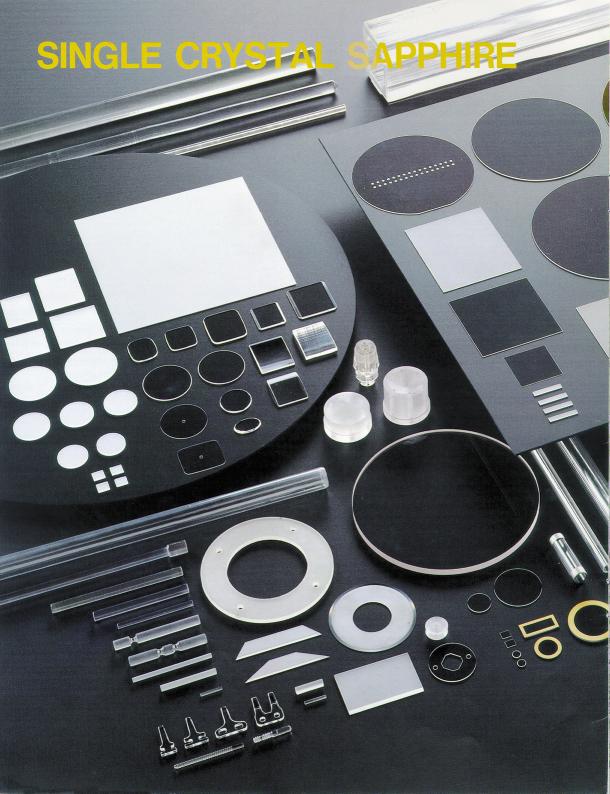
6 SAPPHIRE PRODUCTS Substrate Application (1) SOS (2) Thin Film HIC Substrate (3) Semiconductor Monitor Wafer (4) Semiconductor, Piezoelectric Semiconductor, Superconductor, Thin Film Substrate (5) MR Sensor, Precision Resistor Substrate (6) GaAs and other Substrate Holding Plates Standard Specifications Shape OF Length φ 2 ± ±.5 55 ~ 6 φ 15 ± ±.5 45 ~ 5 φ 125 ± ±.5 4 ~ 45 φ 1 ± ±.5 3 ~ 35 φ 76.2 ± ±.5 19 ~ 25 Optical Products Application (1) POS Scanner Window (Sapphire On Glass) (2) Window Semiconductor Manufacturing Device: Vacuum Equipment, High-Temperature/High-Pressure Container (3) Cap for Optical Communication (4) Infrared Measuring Device Window (5) Coin Sensor (6) Lamp External Tube High-Pressure Sodium, Xenon, Metallic Halide (7) Thermocouple Protection Tube (8) Light Receiving Window Accelerating Tube High-Temperature Measuring Rod SHAPE AND MACHINING ACCURACY Standard Dimensional Tolerance Nominal Dimension 1 a 1 a 4 4 a a a a : a Tolerance (±) Machining accuracy:tube I.A./O.A. and standard tube thickness tolerance ±.25. Hole diameter and standard pitch tolerance ±.1. Shape and Specifications Shape Example of Section Dimensions Crystal Orientation Width: 2max. R Plane: ±2deg Plate t W Length: 3max. A Plane: ±5deg Thickness:.2 ~ 2 C Plane: ±2deg Diameter:.5 ~ 2 C Axis in Longitudinal Rod D Length: 1max. Direction Inside Diameter: 1.3 ~ 5 C Axis in Longitudinal Tube t I.D Tube Thickness:.25 ~ 5 Direction Length: 1max. Others To be decided separately To be decided separately Shapes other than shown above are available.

 Biomaterial (BIOCERAM ) Clamp Ring in Semiconductor Instrument Ultrasonic Microscope Sensor Head BIOCERAM is a registered trademark of KYOCERA.")

7 Watch Window Material Use (1) For Square Model (2) For Circular Model (3) For Cylindrical Model (4) For Large-Size Model (5) For Bezel and Other Ornaments Standard Specifications Finish: Both-Side Grinding. Outside edge as cut. Thickness Tolerance: For square and circular models:±.2 For large-size material: ±.5 Sliding Parts. Blade, Structural Material, Others Application (1) Fiber Bar Guide (2) Blade (for fiber, razor and office goods) (3) Tape Cleaner (4) Insulating Plate and Rod (5) Single Crystal Material Sheet Holder (6) Biomaterial (BIOCERAM ) Clamp Ring in Semiconductor Instrument Ultrasonic Microscope Sensor Head BIOCERAM is a registered trademark of KYOCERA. Finish Finish AS GROWN Grinding Lapping Polishing Surface Roughness-.6TYP..2TYP.1 ( µmra) Surface Roughness ( µmra) For other special specifications, contact Kyocera. JUNCTION WITH OTHER MATERIALS Adhesion to Glass Adhesion to glass is available using EVA sheet adhesive. Brazing to Metal Same as ceramics, brazing can be done to KOV and other materials through metallizing methods. (Ex.: High Vacuum Container Window, Packing, Cap, etc.)