7 µc-si:h n-i-p solar cells on textured Ag ZnO:Al back reflectors
|
|
|
- Posy Cain
- 5 years ago
- Views:
Transcription
1 7 µc-si:h n-i-p solar cells on textured Ag ZnO:Al back reflectors 7.1 Introduction The present study on ZnO:Al and textured Ag back reflectors is aimed at application in thin film µc-si n-i-p solar cells. In the previous chapters we have analyzed and discussed various light trapping schemes consisting of textured Ag and ZnO:Al contacts. We indicated the influence of the ZnO:Al TCO layer and correlated the current enhancement to the morphology of the Ag surface. These observations have given us insight in and understanding of some of the factors that dominate the light trapping, such as the morphology of the light scattering interfaces and the low refractive indices of the TCO contacts. Optimization of this back reflector structure, however, did not show an increased current generation. The current generation showed a saturation level, which indicated that the light reflection could be limited due to other factors. In this chapter we will discuss three aspects that we consider would limit the capacity to achieve larger current generation in the µc-si n-i-p solar cells. 129
2 130 µc-si:h n-i-p solar cells on textured Ag ZnO:Al back reflectors First, as was introduced in the previous chapter, the plasmon absorption of the textured metal layers results in a large loss of the current generation. We will present the effect of the morphology of the metal layer on the parasitic plasmon absorption and discuss some options for how to prevent these losses. At second, as was introduced in Chapter 3, the ZnO:Al TCO layer has been shown to give an enhanced light trapping effect. However, the TCO layers also cause absorption losses. Further we introduced some effects of the ZnO:Al on the Ag plasmon absorption (Section 3.3.3) that will be discussed in more detail in this chapter. Additionally, we mentioned that for this substrate configuration type of solar cells, it is then not straightforward to insert a ZnO:Al layer without changing the structure growing on top of it in a solar cell. This has already been indicated by the effects of a hydrogen plasma presented in Section In this chapter we will show that the interface of ZnO:Al/n-layer is crucial for the developing i-layer and the device performance. At third, in Chapter 6 we mentioned that to a first approximation we have ignored the influence of the different types of rough back contacts with ZnO:Al TCOs on the structure development of the intrinsic layers in the solar cells. In this chapter we have analyzed the dependence of the roughness of the metal contact layers on the J-V parameters of the 1.5 µm thick µc-si solar cells. Furthermore, we will show the results of the transmission electron microscope (TEM) measurements of the layers with various roughness in order to obtain some understanding of the microcrystalline structure evolution and its effect on the solar cell efficiencies. 7.2 Plasmon absorption on the Ag surface In Chapter 5 we described the structures of Ag:AlO x back reflectors, which show large rms roughness in combination with smaller main lateral features sizes. From Section 6.5 we also observed that these samples show a high intensity in the wide angle ars measurements. The combination of large rms roughness, wide angle ars and a high contribution of feature sizes around nm give high weighted values, that should results in higher generated currents. However, as is observed in Figure 7.1b one drawback of some of the Ag:AlO x layers is that they showed a decrease in total reflection. The Figures 7.1a and 7.1b reveal two plasmon absorption peaks [110]. The high absorption at 320 nm is attributed to the bulk plasmon of silver at 3.92 ev. This bulk absorption will be independent of the surface morphology. At 350 nm a weaker surface plasmon peak is observed. This absorption peak will be both material as well as surface morphology dependent. The peak can be broadened and extend up to the long wavelength region, as can be seen in the figures. Figure 7.1a shows five Ag samples having rms roughness in the region from 4 to 111 nm. Compared to the 4 nm roughness Ag layer a large absorption increase and broadening of the SP peak is visible. On the other hand the Ag layers above 67 nm roughness only show among themselves slight variation
3 µc-si:h n-i-p solar cells on textured Ag ZnO:Al back reflectors 131 in peak position and absorption intensity. Compared to flatter Ag layers with rms roughness below 30 nm (not shown), a large increase in absorption over the whole wavelength range is seen (up to % in the range of nm). Both the Ag:AlO x samples with large rms roughness ( nm) and small feature sizes ( nm) show that the surface plasmon peak is shifted to 360 nm and increased in intensity (Figure 7.1b). This increased absorption is extended to the long wavelength region and accounts for more than 10 %. The change in absorption has to be attributed to both material as well as surface changes. Figure 7.1b also shows a 2 µm thick Ag:AlO x layer which still has 60 nm rms roughness. However, due to the thickness of this layer a complete restructuring of the crystal has taken place, as described in Chapter 5. This resulted in extended features sizes of 3500 nm and, as can be seen, this layer again shows lower plasmon absorption. These observations indicate that the surface plasmon absorption in the Ag and Ag:AlO x layers is highly dependent on the morphology and increases with increasing roughness. It reveals that with a certain roughness the plasmon absorption is increased even more if the lateral features sizes are close to the wavelength size. Moreover, from the literature we learnt that there are two ways by which plasmon absorption can be increased: grating coupling [126] and attenuated total reflection [55]: 1) Grating coupling: A surface plasmon can not be generated directly by light. In order to obtain an interaction between light and a surface plasmon both the energy and momentum have to be conserved. One method to circumvent this restriction is by relaxing the momentum conservation due to roughening of the metal surface. If the spatial periodicity of the surface roughness is similar to the wavelength of the reflected light the coupling will be more effective. 2) Attenuated total reflection: With this method the effective wave vector (and hence momentum) of the reflected light is increased. This can be done by using a medium on top of the surface with a higher optical density (higher refractive index). The field that is created on this interface can be coupled to the surface plasmons. These two methods reveal interesting insight in the light trapping effects of rough surfaces and TCO layers: Firstly, the rough surface that we consider to be optimal for light scattering should have feature sizes similar to the effective wavelength that is scattered. However, as we have observed and explained from the grating coupling theory, exactly this morphology will give rise to increased coupling of the light to the surface plasmons (hence increased absorption and loss in reflected light). The increased scattering and increased plasmon coupling are thus two compensating effects. The current generation inside a solar cell is therefore limited when the plasmon absorption dominates. The two Ag:AlO x layers, both of which have optimized morphology for effective light scattering, indeed give a lower current generation, which can be related to the increase in plasmon absorption. In Figures 6.9a and 6.9b of the previous chapter the importance of the effect of the plasmon absorption on the current generation has already been indicated.
4 132 µc-si:h n-i-p solar cells on textured Ag ZnO:Al back reflectors Normalized total reflection intensity (%) SP: 350 nm BP: 320 nm Wavelenght (nm) Ag, σ = 4 nm Ag, σ = 67 nm Ag, σ = 83 nm Ag, σ = 92 nm Ag, σ = 111 nm A Noramlized total reflection intensity (%) SP: 360 nm Ag, σ = 67 nm, L =1700 nm Ag:AlO x, σ = 61 nm, L = 1250 nm Ag:AlO x, σ = 76 nm, L = 830 nm Ag:AlO x, σ = 133 nm, L = 1600 nm Increased Absorption Wavelenght (nm) Energy shift + Increased Absorption Figure 7.1 (a): The total reflection intensity of Ag layers with various rms roughness, σ. The bulk plasmon (BP) absorption peak and surface plasmon (SP) absorption peak are located at 320 and 350 nm respectively. Due to interference, the absorption of the SP peak extends up to the long wavelength region. (b) The total reflection intensity of one Ag layer and three Ag:AlO x layers with different morphology. The two Ag:AlO x layers with high roughness and small feature sizes show an increased BP and SP plasmon absorption and an energy shift of the SP peak position. B
5 µc-si:h n-i-p solar cells on textured Ag ZnO:Al back reflectors 133 Secondly, the theory of attenuated total reflection can explain the effect of a TCO interlayer between the i-layer and metal reflecting contact. As is discussed in Chapter 3 there are several reasons for enhanced light trapping that were ascribed to the insertion of a TCO interlayer, such as interference and scattering on the crystal grains of the TCO. We discussed that these two effects can only be effective if respectively thin (interference) and thick (scattering at crystal grains) TCO layers are used. As was mentioned before, the data in Figure 3.15 suggested that we needed a more convincing explanation. In Chapter 6 we mentioned that the ZnO:Al layer will change the λ eff to larger wavelength values as compared to the λ eff in the silicon i-layer. We discussed how this effect could induce a more efficient scattering at the Ag/TCO interface, because of the rather large lateral feature sizes on the Ag surface. Furthermore, this change in λ eff will also have an effect on the plasmon absorption: the ZnO:Al TCO is a medium with lower optical density, therefore its presence will result in a smaller effective wave vector of the light and, as explained by the attenuated total reflection, decrease the plasmon absorption. With this explanation, a considerable step towards a higher current generation is expected when a TCO layer is inserted and furthermore no difference in current generation will be seen with changing the thickness of the TCO layer. The presented data in Table 3.1 indeed suggested this trend, which strengthens the consideration that the plasmon absorption on rough metal layers strongly influences the light trapping and current generation in the solar cells. 7.3 ZnO:Al TCO interlayer in solar cells The limitations on the enhanced light reflection In the previous section and in Chapter 3 we mentioned several reasons for enhanced reflection and thus current generation with the ZnO:Al back reflector. This section will discuss the limitations of the use of a ZnO:Al TCO that we consider to affect the current enhancement inside the solar cells. First the effect of increased light reflection of light by the use of the interference principle with a λ eff /4 thick TCO layer on top of a flat reflecting contact is limited due to the specular behavior of the reflected light. There will be an increased intensity of light in a specific wavelength region, however, the light will be reflected without an increase of path length and will be lost through the front side of the solar cell. If we introduce a roughness at the interfaces of the TCO and/or Ag layers in order to achieve diffuse light reflection with increased path length, the need for any interference will be lost. The second reason that we have mentioned for increased light reflection is, the additional reflection from the ZnO:Al crystal grains, as was suggested in the literature [53]. This enhanced reflection will, on the other hand, be limited by the additional light absorption in the ZnO:Al layer, as the scattering in the polycrystalline ZnO layer is only increased with thicker layers (and thus more scattering centers). Figure 3.14 has shown the increase in light
6 134 µc-si:h n-i-p solar cells on textured Ag ZnO:Al back reflectors absorption at 800 nm wavelength. This absorption is induced by the free electron absorption in the ZnO:Al layer. Decreasing the electron density is one of the options to decrease the free carrier absorption, which again influences the conduction of the layer in opposite manner. Therefore, the ZnO:Al TCO layer should be kept thin enough in order to avoid the parasitic absorption losses. This will therefore limit the effect of light scattering at the crystal grains. Lastly, as we had discussed above, the effect of decreased plasmon absorption at the Ag layer due to the lower optically dense ZnO:Al layer compared to the high optical density silicon layer also influences the reflection. This, however, also suggests that a still lower density medium, such as air, in front of the Ag surface will further decrease the plasmon absorption. The reflection measurements as depicted in Figure 7.1a and 7.1b actually were measured with an air/ag interface, which therefore probably underestimates the plasmon absorption compared to the ZnO:Al/Ag interface, as is used inside the solar cell. This effect has indeed been observed in the literature: Springer et al. [54] have measured by PDS the plasmon absorption of silver samples and ZnO coated silver samples with different roughness. They observed that the surface plasmon peak is shifted towards longer wavelengths in combination with the ZnO layer. For rough silver surfaces the peak is shifted from 3.5 ev (350 nm) to 2.8 ev (440 nm) and in addition, the long wavelength absorption can be more than doubled on rough metal surfaces compared to flatter surfaces. This result clearly indicates the limitations of ZnO layers on rough surfaces due to plasmon absorption. In order to avoid the parasitic plasmon absorption at the Ag surface we suggest to use materials with even lower refractive index than ZnO:Al, which will not be an easy task as most of these materials (such as oxides) are not good electrical conducters and will induce parasitic resistance losses The limitations on the solar cell performance Table 7.1: The differences in solar cell performance with and without a hydrogen pre-treatment on rough and flat glass/ag/zno:al substrates. Rough Efficciency J sc V oc R FF s R p Ag/ZnO:Al (%) (ma/cm 2 ) (V) (Ωcm 2 ) (Ωcm 2 ) H treatment No H Flat Ag/ZnO:Al H treatment No H An advantage of making µc-si solar cells in n-i-p configuration is that the µc-si n- and i-layer are deposited on top of the Ag and ZnO layers, for which there are no limitations on temperature and deposition power for these layers (as long as the substrate can withstand). This gives one the opportunity to prepare a wide range of different Ag and ZnO:Al layers for back reflector, without damaging the solar cell, as would be the case for p-i-n solar cells.
7 µc-si:h n-i-p solar cells on textured Ag ZnO:Al back reflectors 135 However, one drawback is that the µc-si n-layer and i-layer are deposited on top of a ZnO:Al surface conformal with the Ag roughness and in such a case it is not an easy task to achieve good quality in these silicon layers, as it has been shown that it is difficult to start nucleation on rough ZnO surfaces [67]. For optimal n-i-p µc-si solar cells it is critical that no incubation is present at the bottom i-layer/n-layer region, as this will decrease the current generation in the long wavelength region from the bottom part of the i-layer. Furthermore, the lattice mismatch between the sputtered [001] ZnO (2.60 Å) and CVD [220] silicon (1.92 Å) is more than 30 %, which can induce a lot of stress in the silicon layer and degrade its properties. Lastly, as has been shown in Chapter 3.5, the ZnO:Al is not inert to atomic hydrogen during a plasma deposition, with high hydrogen diluted silane. We have shown with XPS measurements that SiO 2 is created on the ZnO:Al surface during a hydrogen plasma treatment. We have to consider the possibility that Zn particles are created that can easily diffuse through the n- layer/i-layer structure during the solar cell deposition. This will affect the material properties of the solar cell that would limit the current generation. We have prepared many µc-si solar cells with varying Ag/ZnO layers (as reported in this thesis) as well as with many different type of n-layers, because it turned out that a wrong combination of these layers can have deleterious effects on the solar cells performance [104]. As presented by Li et al. thick µc-si n-layers (> 70 nm) on SS/Ag/ZnO substrates show inferior solar cell parameters and increased shunting. The yield improves with decreasing the n- layer thickness down to 24 nm. Furthermore, deposition of the n-layer at lower T sub also resulted in improved solar cell performance. Because the 20 nm thin low T sub n-layer showed higher crystallinity, as is measured by Raman spectroscopy, it suggests an improved nucleation on the ZnO:Al that could have resulted into the improved solar cell performance. In order to create better nucleation sites for the n-layer on the ZnO:Al TCO later we subsequently suggested a hydrogen plasma treatment on the ZnO:Al layer before the solar cell deposition, as this treatment would result in a thin SiO 2 layer on the ZnO:Al surface. We deposited on both flat as well as rough Ag/ZnO:Al the same type of n-i-p µc-si solar cells with a 1.5µm i-layer. The µc-si n-layer was deposited at 200 o C. The performance of both these cells is compared to the cells made with the same recipe, but in addition of a 20 pre-treatment of the TCO with atomic hydrogen (in a pure hydrogen atmosphere) resembling the n-layer deposition. Table 7.1 shows the J-V parameters of cells of comparable thickness. The hydrogen pre-treatment clearly leads to improved solar cell performance. The improvement of the FF is related to an increased light R p and a decrease of light R s. Dark measurements reveal that mainly the i-layer quality has improved as is evident from the improved diode quality factor. The large decrease in R s value for the flat Ag/ZnO:Al was also confirmed by an improved contact resistance in dark measurements. This observation indicates that the SiO 2 layer formed on the ZnO:Al likely improves the n-layer quality and thereby the whole i-layer structure. This again indicates how critical the ZnO:Al/n-layer combination can be for the growth of a high quality µc-si i-layer. Furthermore, a small decrease in dark R p has been observed, which actually indicates that the SiO 2 layer does not decrease the diffusion of
8 136 µc-si:h n-i-p solar cells on textured Ag ZnO:Al back reflectors particles through the shunting paths in the n and i-layers. On the contrary, a lower dark R p value indicates larger shunting paths, likely introduced by the increased crsytallinity in combination with a larger defect density. The above observations indeed infer that the ZnO/n-layer interface is a critical interface that can easily deteriorate the quality of subsequently deposited layers in a solar cell and therefore limit the capacity to achieve high efficiency in µc-si solar cells. 7.4 The influence of roughness on the solar cell parameters 0.58 single 27 nm µc-si n-layer double 5nm a-si + 27nm µc-si n-layer 0.56 V oc ( V ) A B 0.50 C D rms roughness ( nm ) A single 27 nm µc-si n-layer double 5nm a-si + 27nm µc-si n-layer 1E-6 J 0 ( A/cm 2 ) 1E-7 1E rms roughness ( nm ) B
9 µc-si:h n-i-p solar cells on textured Ag ZnO:Al back reflectors 137 diode quality factor N single 27 nm µc-si n-layer double 5nm a-si + 27nm µc-si n-layer rms roughness ( nm ) C single 27 nm µc-si n-layer double 5nm a-si + 27nm µc-si n-layer 1000 Light R p (Ohm cm 2 ) rms roughness ( nm ) Figure 7.2: Solar cells with various rms roughness and/or n-layer. The dependence of: (a) the V oc, (b) dark current density J 0, (c) the diode quality factor n the and (d) the light R p, are shown. D As reported, in Chapter 6 there is no universal correlation between the collected current in n-i-p solar cells and the rms roughness of the substrate surface. A better correlation is visible after combining the lateral feature sizes and correcting for the surface plasmon absorption of the Ag back contacts. In this study we kept the deposition parameters of all silicon layers constant in order to make a trustable comparison. However, while changing the roughness, the properties of the silicon i-layer are also subject to changes. This can be one of
10 138 µc-si:h n-i-p solar cells on textured Ag ZnO:Al back reflectors the reasons for the limitations of the current generation that is seen in the Figure 6.9. In order to clarify the changes in the i-layer we show the dependence of the J-V parameters (V oc, J o, n value and light R p ) on the rms roughness in Figures 7.2a, 7.2b, 7.2c and 7.2d. Note that the highest current values were not achieved with the largest rms roughness. The i-layers are deposited at 250 o C with 5/100 sccm of SiH 4 /H 2 ratio at a processing pressure of 50 µbar. Clearly a decrease in V oc is observed with increasing rms roughness. The closed squares are for cells with a 27 nm µc-si n-layer made at 200 o C. The three samples with open circles are deposited with a double n-layer (5 nm a-si / 27 nm µc-si ), among which samples A and B have a Ag:AlO x substrate layers and also a 500 nm ZnO:Al layer instead of only 100 nm as is the case for all the other cells that are depicted. This double n-layer, however, resulted in a completely amorphous layer as was evident from Raman spectroscopy measurements. It is therefore expected that these samples have a large incubation phase in the bottom part of the i-layer, as it is initially grown on an n-layer that is amorphous. This incubation phase has either a high amorphous fraction and/or a large defect density. The TEM measurements of layer A are shown in Figure 7.3. We indeed observe an amorphous n-layer. A large amorphous incubation phase is not seen, however, the image clearly shows a thin incubation region with very low silicon density (evident from the thin white regions at the interface). This region is presumed to be highly defective. Compared to the samples without a double n-layer recipe, samples A and B showed, after correction of the plasmon absorption, a lack of current collection at long wavelengths. This could result from the defective incubation phase. As is seen in Figure 7.1a and c this amorphous n-layer leads to an increase in V oc for these cells and a slightly lower J 0, as is expected from solar cells with a lower average crystalline fraction in the µc-si i-layer [67]. This observation again indicates that the initial stage of the n- layer growth is critical for the resulting i-layer quality. In Figure 7.1a for the solar cells with the single n-layer, two samples fell out of range with a lower V oc than that the trend shows. The samples are labeled C and D and are deposited in the same run. However, there was no difference in the deposition parameters or wire age for the deposition of these layers compared to the other layers, apart from a two times longer pre-heating time of the filaments and thus the substrate, before the i-layer deposition. This could have resulted in higher crystallinity, because the diode quality factor is also slightly lower and a higher J 0 value is seen. The complete trend in the dark measurements of all the solar cells with back contacts of various roughness, shows an increasing J 0 value at increased rms roughness (Figure 7.1b). The higher J 0 values explain the lower V oc values at higher roughness, as it can be attributed to higher midgap defect density and/or higher crystallinity in the material. Moreover, the increasing n values (Figure 7.1c) with increasing roughness, suggest more drift nature of the cells and confirm a higher defect density. This confirms our speculation that the i-layer is one of the limiting factors for current the increase, as the higher diode quality factor indicates more current loss at the maximum power point. The larger roughness substrates results in inferior i-layer quality.


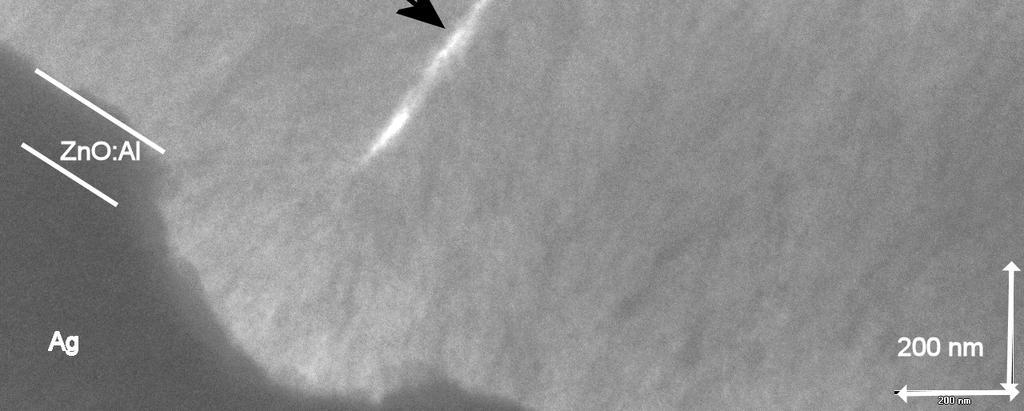
11 µc-si:h n-i-p solar cells on textured Ag ZnO:Al back reflectors 139 Figure 7.3: The cross section of the bottom part of a solar cell. The various layers are indicated. The image reveals an amorphous n-layer with on top a thin incubation layer. This layer is visible by the bright lateral line along the n-layer/i-layer interface, which indicates a low silicon density and defective material. No vertical cracks are observed. One question arises: Why do rougher samples show a higher defect density and inferior quality? In order to find an answer we have analyzed the XTEM pictures of four different solar cells with increasing roughness of the Ag back contact. Figures 7.4a, b, c and d show the results of a cross section of the solar cells with 4, 67, 88 and 135 nm rms roughness respectively. As can be seen in the TEM images the layers with high rms roughness show vertical cracks through the i-layer. These cracks evidently are created in the regions where the substrate surface shows valleys with steep slopes. The cracks are then created at the point where the crystalline conical-shaped grains from the left and right side of this valley are touching each other. A highly defective boundary is created that can even run completely up to the upper ITO layer. Given the fact that the constituent of ITO would likely diffuse during its deposition at elevated temperatures, these cracks will become effective shunting paths. Some of the cracks are already being created from the bottom substrate surface. These cracks do not only grow towards the upper growth direction but are also seen to develop under an angle, as it follows the normal of the slopes of the textured surface. The high defect density can explain the low FF (< 0.6) for all these solar cells and low light Rp values, as seen in Figure 7.1d. Although, the TEM pictures can only reveal a small section ( ± a few microns) of the complete solar cell area, the fact that no cracks were visible on the cells with low ( 4 nm ) roughness substrate, suggests a smaller crack density over the area and therefore can explain the lower J0 and n values. The layer, however, does not show higher light Rp, but the dark J-V measurements do indicate a higher shunting resistance (Figure 7.5). Moreover, one of the solar
 and a thin incubation layer with a low silicon density in the")

12 140 µc-si:h n-i-p solar cells on textured Ag ZnO:Al back reflectors cells gave a high light Rp value around 1000 Ωcm2 and thus higher FF (0.66). Although, this sample has an rms roughness of 76 nm and a high density of valleys (the surface lateral features were small; 850 nm) and a thin incubation layer with a low silicon density in the lateral direction, no long vertical cracks were observed from the TEM pictures (Figure 7.3). The absence of these cracks is in contrast to what is observed in all other large rms roughness layers. Figure 7.5 shows the dark J-V measurements of the solar cells that are shown in the TEM images of Figures 7.3 and 7.4a, b, c and d. It is observed that the solar cells with cracks in the ilayer (visible in TEM), show a decrease in the dark Rp value (J-V data from the low voltage range shifts upwards). Solar cells from Figure 7.3 and 7.4a that did not show any cracks in TEM and therefore likely have a smaller density of shunting paths, show higher dark Rp values. This clearly indicates that a material without any cracks will result in a high quality µc-si i-layer. Finally, we would conclude that both a high Voc as well as a high Jsc is not easy to obtain, as the high Jsc values are obtained with intermediate rms values. Reports from the Neuchâtel group [67] also supports this trend. In order to improve the i-layer quality over the whole layer thickness that would deliver a high Voc, we recommend the use of hydrogen profiling steps. By doing this the i-layer should be deposited just above the transition region over the whole thickness, which can result in lower defect density and crack formation and thus higher Voc. A


13 µc-si:h n-i-p solar cells on textured Ag ZnO:Al back reflectors 141 B C
 4, (b) 67, (c) 88 and (d) 135 nm. The various solar cell layers are indicated.")
 Figure 7.")
14 µc-si:h n-i-p solar cells on textured Ag ZnO:Al back reflectors 142 D Figure 7.4: The cross section of complete solar cells with various rms roughness of Ag substrate layers: (a) 4, (b) 67, (c) 88 and (d) 135 nm. The various solar cell layers are indicated. Additionally, the arrows indicate the cracks that are visible in the i-layer. Dark current density (A/cm ) Decreased dark Rp Figure 7.3, σ = 76 nm Figure 7.4a, σ = 4 nm Figure 7.4b, σ = 67 nm Figure 7.4c, σ = 88 nm Figure 7.4d, σ = 135 nm 1E-3 1E E Voltage (V) Figure 7.5: Dark J-V characteristics of n-i-p solar cells with various roughness, σ of the back contacts. The solar cells with decreased dark Rp values show cracks in the i-layer, observed by TEM in Figures 7.4b, c and d. The solar cells that did not show cracks in the i-layer (Figures 7.3, 7.4a) show increased dark Rp values.
15 µc-si:h n-i-p solar cells on textured Ag ZnO:Al back reflectors 143 The highest efficiency solar that is obtained is presented in Table 7.2. For this solar cell we used a stainless steel substrate with optimized Ag metal contact and 100 nm ZnO:Al TCO back reflector. During the 2000nm i-layer deposition the material quality has been kept more constant by using hydrogen profiling steps in the gas phase. A high efficiency of 8.5 % with a J sc of 23.4 ma/cm 2 has been achieved. Table 7.2: The highest efficiency solar cell on SS/textured Ag/ZnO:Al back reflector with 2µm i-layer. Efficciency J sc V oc R FF s R p (%) (ma/cm 2 ) (V) (Ωcm 2 ) (Ωcm 2 ) Best cell Average best 5 cells Conclusion We have shown three effects that are related to the limitation of the current generation of the solar cells that is visible in saturation or decrease of the current with theoretically optimized back reflectors. These effects are related to the Ag back reflecting layer, the ZnO:Al TCO layer and the i-layer quality. We concluded that the back reflecting Ag:AlO x substrates, which have optimized light scattering morphology also show increased plasmon absorption towards the long wavelength region. The plasmon absorption has been shown to be morphology related and is increased, when a high refractive index layer is placed on top of the metal surface. On the one hand, the ZnO:Al TCO has a lower refractive index than the silicon i-layer and therefore its insertion would decrease the plasmon absorption, compared to the case where the silicon layer is directly deposited on the Ag layer. On the other hand, however, the refractive index of ZnO:Al has still a rather high value of 1.8. This will give limitations to the current generation due to increased plasmon absorption losses of the light. Secondly, we have discussed the development of the n-layer on the ZnO:Al surface, which is considered to be one of the crucial interfaces for the i-layer deposited on it. The mismatch of the lattice constant between the ZnO:Al and silicon layers and the reaction of the ZnO:Al with atomic hydrogen can result in inferior n-layer quality due to difficulty in nucleation. Finally, we showed that the solar cells deposited on larger rms roughness substrates delivered lower V oc values, which is attributed to be a result of increased midgap defect density in the material. XTEM images have shown crack formation through the complete i-layer structure, starting on the slopes of the valleys or above the middle of the valleys, where the conical-shaped grains from the left and right side of the valley are touching. Furthermore, it has been observed that solar cells without any crack formation show high dark R p values and high FF. The increasing defect density and crack formation for solar cells with high rms
16 144 µc-si:h n-i-p solar cells on textured Ag ZnO:Al back reflectors roughness back reflectors are clearly limiting the current collection and the solar cell performance. A better control of the developing i-layer, with hydrogen profiling steps is needed for device quality solar cells on large rms roughness back reflectors. A highest efficiency µc-si:h solar cell of 8.5 % is obtained.