CHARACTERIZATION OF ELECTROTHERMAL ACTUATORS AND ARRAYS FABRICATED IN A FOUR-LEVEL, PLANARIZED SURFACE-MICROMACHINED POLYCRYSTALLINE SILICON PROCESS
|
|
|
- Avis Haynes
- 5 years ago
- Views:
Transcription
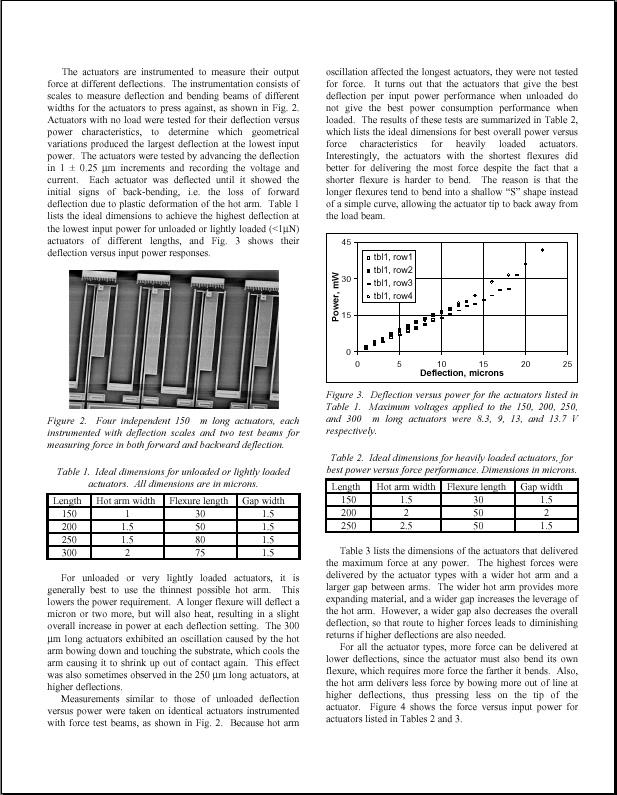
1 CHARACTERIZATION OF ELECTROTHERMAL ACTUATORS AND ARRAYS FABRICATED IN A FOUR-LEVEL, PLANARIZED SURFACE-MICROMACHINED POLYCRYSTALLINE SILICON PROCESS John H. Comtois*, M. Adrian Michalicek*, and Carole Craig Barron** *U.S. Air Force Phillips Laboratory, KAFB, NM **U.S. Department of Energy, Sandia National Laboratories, KAFB, NM SUMMARY This paper presents the results of tests performed on a variety of electrothermal microactuators and arrays of these actuators recently fabricated in the four-level planarized polycrystalline silicon (polysilicon) SUMMiT process at the U. S. Department of Energy s Sandia National Laboratories [1]. These results are intended to aid designers of thermally actuated mechanisms, and will apply to similar actuators made in other polysilicon MEMS processes. The measurements include force and deflection versus input power, maximum operating frequency, effects of long term operation, and ideal actuator and array geometries for different design criteria. A typical application in a stepper motor is shown to illustrate the utility of these actuators and arrays. Keywords: microactuators, electrothermal, SUMMiT ELECTROTHERMAL MICROACTUATORS The basic device studied in this research is a singlematerial actuator which deflects at its tip by unequal thermal expansion of its constituent parts. A typical U shaped electrothermal actuator is shown in Fig. 1. Current is passed through the actuator via the anchors, and the higher current density in the narrower hot arm results in greater ohmic heating, causing it to expand more than the wider cold arm. The arms are joined at the free end, which constrains the actuator tip to move laterally in an arcing motion towards the cold arm side [2,3]. Backwards deflection can be achieved by momentarily over-driving the hot arm which causes it to deform plastically, decreasing its overall length. The actuator then bends backwards past its initially fabricated position when the power is removed. The actuator can therefore deliver a static force, or it can be operated in the forward direction from its new starting position [4]. Hot arm Cold arm Direction of motion Dimple Anchor Flexure Figure 1. Schematic view of an electrothermal actuator. This simple actuator can be fabricated in any MEMS process that includes at least one releasable, current carrying layer. A typical 200 µm long actuator is capable of 16 µm of deflection when unloaded, and can deliver up to 13 µn of force. Arrays of actuators allow the generation of many 10 s of µn of force. Most importantly, these actuators operate in a current and voltage regime which is directly compatible with standard CMOS electronics, e.g. 0 to 14 volts at 0 to 5 ma, depending on the geometry and maximum deflection desired. SUMMiT FABRICATION PROCESS The devices presented in this paper were fabricated in the SUMMiT (Sandia Ultra-planar Multi-level MEMS Technology), through the SAMPLE (Sandia Agile MEMS Prototyping, Layout tools, and Education) service [5]. As in other surface-micromachining processes, the devices are formed in SUMMiT by the alternate deposition of structural polysilicon layers and sacrificial oxide layers, over a base nitride layer. These devices were etched in a 1:1 mix of HF:HCL and dried in supercritical carbon dioxide process. The complexity of the micromachines which can be manufactured in a given process is a function of the number of independent layers of structural polysilicon the technology provides. Although the actuators presented in this paper require only one releasable structural layer, complex applications of them usually require more. Geared mechanisms, for example, require two independent levels (one to form the hubs and the other the moving gears), and reduction-geared mechanisms require three independent levels. Unique advantages of the SUMMiT process include one-micron feature sizes, planarization of the third polysilicon level, and the ability to make flanged gear hubs and electrical contacts to the substrate. SINGLE ACTUATOR TESTS This section reports the condensed results of tests performed on single actuators of 90 slightly different geometries. The variations are used to pinpoint the ideal geometry for applications requiring different deflections and forces. The actuators fall into 4 categories by overall length, and within those categories are variations of hot arm width, flexure length and the width of the gap between the two arms. All of the actuators are made of stacked Poly-1 and Poly-2 because the thicker polysilicon layer puts the overall device resistance into a range that makes it CMOS-compatible, i.e. a cold resistance in the range of 0.5 to 3 kilohms.
2

3

4
5 ACKNOWLEDGEMENT The portion of this work done at Sandia National Labs was supported by the U.S. Dept. of Energy under contract DE-AC04-94AL Sandia is a multiprogram laboratory operated by Sandia Corporation, a Lockheed Martin Company, for the U.S. Dept. of Energy. REFERENCES [1] R. Nasby, J. Sneigowski, J. Smith, S. Montague, C. Barron, W. Eaton and P. McWhorter, Solid State Sensors and Actuators Workshop 96, Hilton Head SC, pp [2] H. Guckel, J. Klein, T. Christenson, K. Skrobis, M. Laudon, and E. G. Lovell,, Solid State Sensors and Actuators Workshop 92, Hilton Head SC, pp [3] J. Comtois and V. Bright, Solid State Sensors and Actuators Workshop 96, Hilton Head SC, pp [4] J. Comtois, V. Bright, and M. Phipps, SPIE 95 vol. 2639, pp [5] Sandia National Laboratories Web Page: