Flip Chip Bump Electromigration Reliability: A comparison of Cu Pillar, High Pb, SnAg, and SnPb Bump Structures
|
|
|
- Brianna Dixon
- 5 years ago
- Views:
Transcription


1 Flip Chip Bump Electromigration Reliability: A comparison of Cu Pillar,,, and SnPb Bump Structures Ahmer Syed, Karthikeyan Dhandapani, Lou Nicholls, Robert Moody, CJ Berry, and Robert Darveaux Amkor Technology 1900 S Price Road Chandler, AZ Abstract Electromigration tests are conducted on,, SnPb and Cu Pillar Flip Chip bumps to determine the relative performance of different bump metallurgies on current carrying capacity. A special test vehicle was designed and tests are being conducted for three (3) different current levels at three (3) temperature conditions. Although complete data is not available at the time of writing this paper, the data to date is summarized in this paper. Introduction Electromigration failure in flip-chip bumps has emerged as a major reliability concern due to potential elimination of Pb from flip-chip bumps and a continuous drive to increased IO density resulting in a reduction of bump pitch and size. Traditionally, flip-chip interconnects had incorporated a high Pb bump soldered with a SnPb eutectic paste to the substrate or another die. However, because of RoHS directives, the industry is responding with Pb free bump development, such as bump with SAC solder or Cu Pillar with SAC/ solder. Although a number of recent publications deal with electromigration reliability of Hi Pb, Pb free, and Cu Pillar bumps [1-5], a gap exists in terms of their performance comparison on the same bump geometry. The available test data is based on different test vehicles and it becomes difficult to determine the relative performance of these different metallurgies under accelerated test conditions. In addition, not all published data provides the essential parameters of Black s equation to determine the performance and reliability for actual use conditions. This paper attempts to fill this gap by comparing electromigration performance of, SnPb eutectic,, and Cu Pillar bumps using the same test vehicle. A special test vehicle was designed with daisy chain structures for electromigration testing and the packages were assembled on test cards. The testing is being done using five (5) stress conditions (combination of current and temperature) to estimate the current density exponent, n, and the activation energy, Ea, parameters for Black s equation. The reliability data of up to 1500 hours of testing is presented in the paper. Test Vehicle The test vehicle used to compare the electromigration performance of varying bump alloys employed a 14.7mm silicon die fabricated using 65ηm technology with low-k dielectric with 150 micron bump pitch. The die is passivated using polyimide with a 47 micron polyimide opening. The bump alloy was varied in order to give a direct comparison of electromigration performance. The bump alloys evaluated were SnPb eutectic,, and Pb-free bump. In each case, the bump was fabricated directly over the polyimide via and adjacent polyimide passivation. The under bump metallization (UBM) diameter of 90 micron was used for this test vehicle with a target bump height of 75 microns. For Cu pillars, 50um of Cu was plated up on sputtered TiW/Cu layers. The top diameter of Cu pillar was 90 micron, same as the UBM diameter for solder bumped parts. The Cu pillars were then plated with 20 and 40um solder to form solder caps. Figure 1: Bump layout on die (14.7 x 14.7mm) and top view of substrate (42.5 x 42.5mm).
.")


2 The dice were attached to an organic laminate consisting of a build up structure with a 400μm thick core. Two different substrates pad types were used; SMD and NSMD. The solder resist opening for SMD pad or the metal pad diameter for NSMD pads were 85 microns. The pads on the substrates were covered with solder (SOP). Finally, SAC305 solder balls were attached on the bottom side of the substrate. Figure 1 shows the bump layout on the die and the top view of the substrate. Table 1 shows the metallurgical details of each test vehicle. Test Vehicle Solder Bump SOP Alloy Substrate Pad Type BGA Balls Table 1: Metallurgical details of 5 flip chip bump configurations used for EM testing Eutectic SnPb Pb Free Cu Pillar SMD Cu Pillar NSMD 95/5 Pb/Sn 63/37 Sn/Pb 2.3 Cu Pillar + Cu Pillar + 40um 20um Cap Cap 63/37 Sn/Pb 63/37Sn/Pb SAC305 SAC305 SAC305 SMD SMD SMD SMD NSMD SAC305 SAC305 SAC305 SAC305 SAC305 The test vehicle used for EM testing has multiple EM structures but a 2-bump daisy chain was used in this particular case. Figure 2 shows the EM structure with electron flow direction. The biggest advantage of using a 2- bump daisy chain structure is that both substrate and die side metallurgies are stressed at the same level and failure on one side causes the failure of the whole structure. This is also useful when the increase in resistance is used as the failure criteria as this increase will be primarily caused by failure of one bump as opposed to many bumps for multiple bump daisy chains. Cathode Die Anode Anode Substrate Cathode Figure 2: Electromigration test structure used for EM testing The assembled packages were soldered to specially designed 1.6mm thick EM test boards which were fabricated using high temperature material to eliminate failures in the board due to high current and temperature. The packages were pre-conditioned (125C bake + 3X reflow) before board attachment. Since SAC305 solder balls were used for the packages, the peak reflow temperature for board assembly was around 240C. It should be noted that this high temperature reflow used for package ball attach, pre-conditioning, and attachment to the board resulted in more mixing of solder with eutectic SnPb SOP compared to a rather clear demarcation of bump and eutectic SnPb solder as observed when low temperature reflow process is used for SnPb ball and board attachment. Test Matrix and Procedure All the test samples are designed as a single bump structures in accordance with JEP154. In order to estimate Black s equation parameters (n and Ea), a combination of 5 temperature and current conditions were used in this study for Cu Pillar SMD,, and SnPb bumps. Due to limited component availability for bumps, only 4
3 stress conditions were used for this particular bump configuration. The stress conditions are shown in Table 2. Eight (8) samples are on test for each stress condition. Table 2: Stress conditions and test matrix Temp (deg C) / Current (Amps) 0.4 Amps 0.55 Amps 0.7 Amps Cu Pillar SMD 135 C Cu Pillar NSMD Cu Pillar SMD Cu Pillar SMD Cu Pillar SMD 150 C 165 C Cu Pillar SMD. The devices under test (DUT) are being tested under constant stress current and temperature. The resistance of the bump electromigration structure (EM device) is measured using a 4-point measurement technique. Special test equipment is used, which is capable of measuring the 4-point resistance measurement with high precision. The test equipment is also capable of computing "Joule Heating Effect" which refers to the increase in device temperature due to current stressing. The testing system automatically performs a Temperature Coefficient of Resistance (TCR) calculation done for each stress current and for each DUT. The temperature increase due to Joule heating was measured as 3.4 o C (Range: o C) and 7.3 o C (Range: o C) for 400 and 700mA current stressing, respectively. Since various DUTs with different current stressing were tested in the same oven for a particular temperature condition, the oven temperature was adjusted down by 5 o C to achieve an average DUT temperature as per temperature conditions listed in Table 2. The EM test device used here was also designed with temperature sensor located above the bump under test and this was used to re-confirm the temperature increase due to Joule heating. The temperature increase due to current measured using this thermal sensor was in the same range as listed above. A 4-point Kelvin measurement scheme was adopted to measure the daisy chain resistance of the 2-bump structure through out the test and a 10% increase in resistance was used as failure criteria for device failures. The initial resistance of the EM structure using 4-point method was measured as 48 to 51mohms. Figure 3 shows a typical resistance increase vs. time curve and the failure criteria used. 100 % Increase in Resistance Failure Criteria > 10% increase in resistance 0 Test Time Figure 3: Typical resistance increase vs. time curve and failure criteria used
4 Results and Discussion To date, a total of 1540 and 470 hours of testing has been completed on temperature conditions of 150 o C and 135 o C, respectively. The test at 165 o C has not been started yet due to equipment unavailability. Table 3 provides a summary of results obtained so far for each bump configuration and stress condition. Bump Configuration Table 3: Result summary for bump configurations and stress conditions Stress Current (ma) Temperature (deg C ) # Samples # Failed Test Hours Completed Cu Pillar SMD Cu Pillar SMD Cu Pillar SMD Cu Pillar SMD As expected, SnPb eutectic bumps were earliest to fail with almost all samples failed at 150 o C condition. Figure 4 shows lognormal distribution of these failures with a clear dependence on current level. The mean life for failed samples at 400 milliamps is almost 4X higher than that for 700 milliamps current stressing at 150C. Failure analysis result of one sample, shown in Figure 5, indicates almost complete depletion of UBM when the UBM is on the cathode side. Also, almost a complete separation of Sn and Pb phases can be observed with Pb moving to the anode side of this bump. The substrate side also shows significant Cu consumption when the substrate is the cathode side Lognormal SnPb_150_400 Cumulative % Failed Hours to Failure L2 R RX - SRM MED F=7 / S=1 SnPb_150_700 L2 R RX - SRM MED F=8 / S=0 μ1=7.1493, σ1=0.1895, ρ= μ2=5.7828, σ2=0.3932, ρ= Figure 4: Lognormal distribution of failures on SnPb for 400 and 700mA condition at 150C
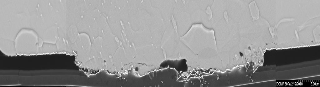
5 Sn Rich Pb Rich Figure 5: Failure analysis of one SnPb failure. Failure observed on the UBM side Surprisingly, bumps failed significantly earlier than expected (some failures are even earlier than SnPb failures). One possible reason is the amount of mixing achieved between high Pb bump and eutectic SnPb SOP during SAC305 solder ball attach and subsequent pre-conditioning and board attach process due to higher reflow temperatures. This is shown in the x-section of unstressed bump in Figure 6a. The failure primarily occurred on the substrate side (cathode) with crack between the large chunks of Cu-Sn intermetallic and substrate Cu pad, as shown in Figure 6b. Further analyses are in progress to determine the cause of early failures of bumps. Pb Rich Sn Rich Cu-Sn_Ni IMC (a) (b) Figure 6: bump: (a) unstressed bump, (b) Failure on substrate side (cathode) A couple of failures were also observed on bump. Failure analysis of first failure indicates a complete depletion of UBM on chip side (Cathode), as shown in Figure 7. Except for one early failure, no additional failures are observed for Cu Pillar bump structure. This indicates significantly better EM performance of Cu Pillar compared to SnPb,, and bumps. This is primarily due to thick Cu Pillar which tends to minimize the current crowding effect at the solder joint level.
6 e-