DEC SA-110S StrongARM 32-Bit Microprocessor
|
|
|
- Emery Rice
- 5 years ago
- Views:
Transcription
1 Construction Analysis DEC SA-110S StrongARM 32-Bit Microprocessor Report Number: SCA Global Semiconductor Industry the Serving Since N. 75th Street Scottsdale, AZ Phone: Fax: Internet:
2 INDEX TO TEXT TITLE PAGE INTRODUCTION 1 MAJOR FINDINGS 1 TECHNOLOGY DESCRIPTION Assembly 2 Die Process and Design 2-3 ANALYSIS RESULTS I Assembly 4 ANALYSIS RESULTS II Die Process and Design 5-7 ANALYSIS PROCEDURE 8 TABLES Overall Evaluation 9 Package Markings 10 Wirepull Results 10 Die Material Analysis 10 Horizontal Dimensions 11 Vertical Dimensions 12 - i -
3 INTRODUCTION This report describes a construction analysis of the DEC SA-110S, 32-bit RISC Microprocessor (200 MHz). Two decapped devices were received independently and three devices, packaged in 144-pin Thin Quad Flat Packs (TQFP), were received from DEC for the analysis. The packaged devices were date coded MAJOR FINDINGS Questionable Items: 1 None. Special Features: Three level metal with tungsten plugs. Apparent CMP planarization. Sub-micron gate lengths (0.25 micron). Cobalt salicided diffusion structures. 1 These items present possible quality or reliability concerns. They should be discussed with the manufacturer to determine their possible impact on the intended application
4 TECHNOLOGY DESCRIPTION Assembly: The devices were packaged in 144-pin Thin Quad Flat Packs (TQFP). Lead-locking provisions (anchors) at all pins. Lead-locking holes at paddle tie bars. Pins 53 and were not connected. Wirebonding method: A thermosonic ball bond technique employing 1.3 mil gold wire was used. Dicing: Sawn (full depth) dicing. Die attach: A silver epoxy compound. Die Process Fabrication process: Selective oxidation CMOS process employing N-wells in a P- epi on a P substrate. Die coat: No die coat was used on the device. Final passivation: A layer of nitride over a layer of silicon-dioxide. Metallization: Three levels of metal defined by standard dry-etch techniques. All levels consisted of aluminum with titanium-nitride caps. Tungsten plugs (stacked when needed) were used as the vertical interconnect under all metals. All plugs appeared to have been lined with titanium-nitride. Intermetal dielectrics: Both intermetal dielectrics consisted of the same oxide structure. A layer of glass was deposited and subjected to an etchback. This was - 2 -
5 TECHNOLOGY DESCRIPTION (continued) then followed by a relatively thick layer of glass which was apparently subjected to CMP and followed by another layer of glass. No SOG layers were used. Pre-metal dielectric: The dielectric consisted of a thick layer of glass (apparently subjected to CMP) over a thin doped layer of glass and densified oxides. Polysilicon: A single layer of dry-etched polycide (poly and cobalt-silicide) was used. This layer was used to form all gates on the die and word lines in the array. Diffusions: Implanted N+ and P+ diffusions formed the sources/drains of transistors. Cobalt silicide was present on all diffusions. Nitride sidewall spacers were used to provide the LDD spacing. Wells: N-wells in a P-epi on a P substrate. Memory cells: Data and instruction cache memory (16KB each) cell arrays were employed. The memory cells used a 6T CMOS SRAM cell design. Metal 3 was not used directly in the cells. Metal 2 formed the bit lines using metal 1 links. Metal 1 was used as cell interconnect and to distribute GND and Vcc. Polycide formed the word lines, select and storage gates. Design features: Slotted Metal 3 bus lines were employed for stress relief. Beveled corners were also used for stress relief. Bond pad structures employed all metal levels with multiple vias. No anti-dishing structures were present
6 ANALYSIS RESULTS I Assembly: Figures 1-6 Questionable Items: 1 None. Special Features: None. General Items: Overall package: The device was packaged in a 144-pin Thin Quad Flat Pack. Die/paddle fit was good. Wirebonding method: A thermosonic ball bond technique employing 1.3 mil gold wire was used. Wire clearance was normal. All bonds were well formed and placed. Bond strengths were normal as determined by wire pull tests. Bond pad structures employed all metal levels with multiple vias (plugs). Dicing: Sawn (full depth). No large chips or cracks were noted. Die attach: A silver epoxy compound of normal quality. 1 These items present possible quality or reliability concerns. They should be discussed with the manufacturer to determine their possible impact on the intended application
7 ANALYSIS RESULTS II Die Process and Design: Figures 7-40a Questionable Items: 1 None. Special Features: Three level metal with tungsten plugs. Apparent CMP planarization of pre-metal and intermetal dielectrics. Short gate lengths (0.25 micron). Cobalt salicided diffusion structures. General Items: Fabrication process: Selective oxidation CMOS process employing N-wells in a P- epi on a P substrate. Process implementation: Die layout was clean efficient. Alignment was good at all levels. Die surface defects: None. No contamination, toolmarks or processing defects were noted. Final passivation: A layer of nitride over a layer of silicon-dioxide. Passivation coverage was good over the topology of the die. Edge seal was also good, as the passivation extended past the metal at the die edge. All three metals were used as part of the edge seal structure. 1 These items present possible quality concerns. They should be discussed with the manufacturer to determine their possible impact on the intended application
8 ANALYSIS RESULTS II (continued) Metallization: Three levels of metallization. All three levels consisted of aluminum with titanium-nitride caps. Tungsten plugs were employed under all metals. Metal patterning: All metal layers were defined by a dry etch of good quality. Metal lines were not widened at vias or contacts; however, the metal completely surrounded the plugs. Metal defects: None. No voiding, notching or cracking of the metal layers was found. No silicon nodules were found following removal of the aluminum. Metal step coverage: Virtually no metal thinning was noted. The tungsten plugs were nearly level with the oxide surface, so no large steps were present for the metal to cover. For reference, MIL-STD-883D allows up to 70 percent metal thinning for contacts of this size. Vias and contacts: All via and contact cuts were defined by a dry-etch. Slight overetching of the vias (M3 and M2) was present; however, no concern exists. A titanium-nitride contact and via liner material was visible at all plugs. Plugs were stacked at all levels where needed. Some small metal 1 and 2 pads were used for via lands (see Figures 19 and 20). No special local interconnect layer was used. Intermetal dielectrics: Both intermetal dielectrics consisted of the same oxide structure. A layer of glass was deposited and subjected to an etchback. This was then followed by a relatively thick layer of glass which was apparently subjected to CMP and followed by another layer of glass. No SOG layers were used. No problems were found. Pre-metal dielectric: This dielectric consisted of a thick layer of glass over a thin doped layer of glass and densified oxides. It appears that the thick layer had been subjected to CMP. No problems were found
9 ANALYSIS RESULTS II (continued). Polysilicon: A single level of polycide (poly and cobalt-silicide) was employed. Polycide formed all gates on the die and word lines in the array. Small gates (0.25 micron) were used throughout the circuitry for both N-channel and P-channel transistors (see Figures 32 and 33). Definition was by a dry etch of good quality. Nitride sidewall spacers were used throughout and left in place. No problems were found. Isolation: LOCOS (local oxide isolation). No problems were noted and no step was noted at the well boundaries. This oxide was relatively thin (0.25 micron) and etched back to be planar with the surface. Diffusions: Implanted N+ and P+ diffusions were used for sources and drains. Diffusions were silicided with cobalt. No problems were noted. Wells: N-wells were used in a P-epi on a P substrate. No problems were noted. Buried contacts: Direct poly-to-diffusion (buried) contacts were not used. Memory cells: Data and Instruction Cache memory cell arrays (16KB each) were employed on the device. The memory cells consisted of a 6T CMOS SRAM cell design. Metal 3 was not used directly in the cells. Metal 2 formed the bit lines using metal 1 connection links. Metal 1 was used as cell interconnect and distributed Vcc and GND. Polycide formed the word lines, select and storage gates. Cell size was measured to be 4 x 6.1 microns (24.4 mm 2 )
10 PROCEDURE The devices were subjected to the following analysis procedures: External inspection X-ray Decapsulate SEM of passivation and assembly Passivation integrity test (chemical) Wirepull test Passivation removal SEM inspection of metal 3 Metal 3 removal and inspect tungsten plugs Delayer to metal 2 and inspect Metal 2 removal and inspect tungsten plugs Delayer to metal 1 and inspect Metal 1 removal Delayer to polycide/substrate and inspect Die sectioning (90 for SEM) * Measure horizontal dimensions Measure vertical dimensions Die material analysis * Delineation of cross-sections is by silicon etch unless otherwise indicated
11 OVERALL QUALITY EVALUATION: Overall Rating: Good DETAIL OF EVALUATION Package integrity G Die placement G Die attach quality N Wire spacing N Wirebond placement N Wirebond quality N Dicing quality N Wirebond method Thermosonic ball bonds using 1.3 mil gold wire. Die attach method Silver-epoxy Dicing Sawn (full depth) Die surface integrity: Toolmarks (absence) Particles (absence) Contamination (absence) Process defects (absence) General workmanship Passivation integrity Metal definition Metal integrity Metal registration Contact coverage Contact registration G G G G G G G G N N N G = Good, P = Poor, N = Normal, NP = Normal/Poor - 9 -
12 PACKAGE MARKINGS TOP Samples 1-3 (Logo) TM Strong ARM TM SA-110S Dec 1995 DC1035 JD0655 A9701 ARM 200 WIREPULL TEST Sample 1 # of wires tested: 20 Bond lifts: 0 Force to break - high: 12.5g - low: 5g - avg.: 9.5g - std. dev.: 2.2 DIE MATERIAL IDENTIFICATION Overlay passivation: Metallization 3-1: Intermetal dielectrics: Plugs (M1 - M3): Pre-metal glass: Polycide: Diffusions: Nitride over silicon-dioxide Aluminum with a titanium-nitride cap. Three layers of silicon-dioxide (possible CMP planarization). Tungsten. Silicon-dioxide. Cobalt-silicide on poly. Cobalt salicide
13 HORIZONTAL DIMENSIONS Die size: 6.4 x 7.7 mm (250 x 305 mils) Die area: 49 mm 2 (76,250 mils 2 ) Min pad size: 0.1 x 0.1 mm (4 x 4 mils) Min pad window: 0.09 x 0.09 mm (3.7 x 3.7 mils) Min pad space: 10 microns Min metal 3 width: 1.5 micron Min metal 3 space: 1.2 micron Min metal 3 pitch: 2.75 microns Min metal 2 width: 0.6 micron Min metal 2 space: 0.6 micron Min metal 2 pitch: 1.2 micron Min metal 1 width: 0.6 micron Min metal 1 space: 0.6 micron Min metal 1 pitch: 1.2 micron Min via (M3-to-M2): 0.75 micron (round) Min via (M2-to-M1): 0.5 micron (round) Min contact: 0.55 micron (round) Min polycide width: 0.25 micron Min polycide space: 0.5 micron Min gate length * - (N-channel): 0.25 micron - (P-channel): 0.25 micron SRAM cell size: 24.4 microns 2 SRAM cell pitch: 4 x 6.1 microns * Physical gate length
14 VERTICAL DIMENSIONS Die thickness: 0.4 mm (15 mils) Layers Passivation 2: 0.6 micron Passivation 1: 0.35 micron Metal 3 - cap: 0.1 micron - aluminum: 1.5 micron - plugs: 1.4 micron Intermetal dielectric 2 - glass 3: Metal 2 - cap: 0.9 micron - glass 2: micron - glass 1: 0.3 micron - aluminum: 0.6 micron - plugs: 0.9 micron Intermetal dielectric 1 - glass 3: Metal 1 - cap: 0.05 micron (approx.) 0.3 micron - glass 2: micron - glass 1: 0.35 micron - aluminum: 0.6 micron 0.05 micron (approx.) - plugs: micron Pre-metal glass - glass 2: Polycide - silicide: Local oxide: 0.9 micron (avg.) - glass 1: 0.27 micron 0.07 micron - poly: 0.2 micron 0.25 micron N+ S/D diffusion: 0.15 micron P+ S/D diffusion: 0.15 micron N-well: 1.2 micron (approx.) P-epi: 3 microns
15 INDEX TO FIGURES PACKAGE PHOTOGRAPH AND ASSEMBLY Figures 1-6 DIE LAYOUT AND IDENTIFICATION Figures 7-9 PHYSICAL DIE STRUCTURES Figures 10-40a COLOR DRAWING OF DIE STRUCTURE Figure 36 CACHE SRAM ARRAY Figures 37-40a - ii -


16 PIN 1 Figure 1. Package photograph and x-ray view of the DEC SA-110S StrongARM. Mag. 3.5x


17 DIE ATTACH ATTACKED DURING DECAPSULATION Mag. 150x EDGE OF PASSIVATION Mag. 1000x Figure 2. SEM views of a die corner and edge seal. 60.

18 EDGE OF PASSIVATION METAL 3 SCRIBE LANE Mag. 2000x EDGE OF PASSIVATION METAL 3 METAL 2 M1 PLUG Mag. 8000x Figure 3. SEM section views of the edge seal structure.


19 Au WIRE LEADFRAME Mag. 525x Au WIRE BOND PAD Mag. 775x Figure 4. SEM views of typical wirebonds. 60.


20 METAL 3 METAL ATTACKED DURING DECAPSULATION BALL BOND DEC SA-110S StrongARM METAL 2 TO CIRCUITRY METAL 3 Mag. 4000x PAD WINDOW METAL 3 TO CIRCUITRY METAL 2 Mag. 8400x Figure 5. SEM section views of the bond pad structure.


21 METAL 3 METAL 2 (FROM PAD) Mag. 5000x N+ DEEP DIFFUSION METAL 2 M2 PLUG M1 PLUG Mag. 10,000x N+ DEEP DIFFUSION M1 PLUG Mag. 26,000x LOCOS N+ DEEP DIFFUSION Figure 6. SEM section views of the input structure.

22 Figure 7. Whole die photograph of the DEC SA-110S StrongARM. Mag. 25x

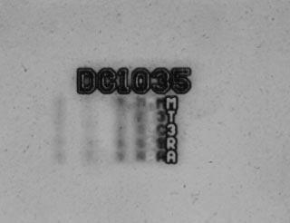
23 Figure 8. Die identification markings. Mag. 800x.


24 Figure 9. Optical views of the die corners. Mag. 100x.


25 PASSIVATION 2 METAL 3 M3 PLUG Mag. 9000x M1 PLUGS POLYCIDE GATES N+ S/D PASSIVATION 2 METAL 3 Mag. 10,000x POLYCIDE GATES N+ S/D PASSIVATION 2 METAL 3 M3 PLUG M2 PLUGS Mag. 10,000x METAL 2 M1 PLUG Figure 10. Silicon etch section views illustrating general structure.


26 PASSIVATION 2 METAL 3 IMD 2 METAL 2 IMD 1 M1 PLUG POLYCIDE GATES METAL 3 IMD 2 METAL 2 M2 PLUG IMD 1 PRE-METAL DIELECTRIC M1 PLUG PASSIVATION 2 METAL 3 IMD 2 M2 PLUG METAL 2 IMD 1 M1 PLUG POLYCIDE GATES Figure 11. Glass etch section views illustrating general structure. Mag. 9000x.


27 PASSIVATION 2 PASSIVATION 1 METAL 3 IMD 2 Mag. 13,000x PASSIVATION 2 PASSIVATION 1 TiN CAP ALUMINUM 3 Mag. 26,000x Figure 12. SEM section views of metal 3 line profiles.


28 Mag. 2400x METAL 3 Mag. 3100x Figure 13. Topological SEM views of metal 3 patterning. 0.


29 Mag. 3500x METAL 3 Mag. 12,000x Figure 14. SEM views of general metal 3 coverage. 60.


30 M3 PLUGS METAL 2 Mag. 22,000x M3 PLUGS METAL 2 Mag. 28,000x Figure 15. SEM views of metal 3 plugs. 55.


31 PASSIVATION 2 METAL 3 M3 PLUG METAL 2 Mag. 15,000x METAL 3 M3 PLUG IMD 2 METAL 2 Mag. 17,000x Figure 16. SEM section views of metal 3-to-metal 2 vias.


32 METAL 3 M3 PLUG METAL 2 Mag. 15,000x IMD 2 TiN CAP ALUMINUM 2 Mag. 26,000x Figure 17. SEM section views of metal 2 line profiles.


33 Mag. 4400x METAL 2 M3 PLUGS M2 CONTACTS Mag. 5000x Figure 18. Topological SEM views of metal 2 patterning. 0.


34 M3 PLUGS METAL 2 Mag. 7000x M3 PLUG Mag. 25,000x METAL 2 M2 PLUG M3 PLUG ALUMINUM 2 Mag. 25,000x CAP M2 PLUG Figure 19. SEM views of metal 2 coverage. 55.


35 M2 PLUG Mag. 25,000x M2 PLUGS M1 PLUGS Mag. 30,000x Figure 20. SEM views of metal 2 plugs. 60.


36 METAL 2 IMD 1 M2 PLUG Mag. 20,000x M1 PLUG POLYCIDE METAL 2 IMD 1 Mag. 26,000x M2 PLUG METAL 2 IMD 1 Mag. 28,000x Figure 21. SEM section views of metal 2-to-metal 1 vias.


37 METAL 2 M1 PLUG PRE-METAL DIELECTRIC Mag. 15,000x IMD 1 TiN CAP ALUMINUM 1 Mag. 40,000x Figure 22. SEM section views of metal 1 line profiles.


38 M2 PLUGS M2 PLUGS Figure 23. Topological SEM views of metal 1 patterning. Mag. 8000x, 0.


39 M2 PLUGS M1 PLUG POLYCIDE Mag. 9000x POLYCIDE Mag. 10,000x Figure 24. SEM views of general metal 1 coverage. 55.


40 CAP ALUMINUM 1 POLYCIDE M1 PLUG Mag. 22,000x POLYCIDE GATE M1 PLUGS Mag. 27,000x Figure 25. SEM details of metal 1 contacts. 60.


41 MI PLUG PRE-METAL DIELECTRIC POLYCIDE LOCOS metal 1-to-polycide Co SILICIDE M1 PLUG POLYCIDE GATE metal-to-diffusion Figure 26. Glass etch section views of metal 1 contacts. Mag. 32,000x


42 IMD 1 M1 PLUGS Mag. 26,000x POLYCIDE LOCOS INCOMPLETE FILL Mag. 35,000x M1 PLUG POLYCIDE LOCOS Mag. 35,000x M1 PLUG POLYCIDE LOCOS Figure 27. SEM section views of metal 1-to-polycide contacts.


43 M1 PLUG POLYCIDE GATE N+ S/D P+ metal 1-to-N+ M1 PLUG POLYCIDE GATE P+ S/D metal 1-to-P+ Figure 28. SEM section views of metal 1-to-diffusion contacts. Mag. 35,000x.


44 POLYCIDE GATES P-CHANNEL Mag. 5700x N-CHANNEL POLYCIDE GATES P+ P-channel, Mag. 10,000x N+ POLYCIDE GATE N-channel, Mag. 10,000x Figure 29. Topological SEM views of polycide patterning. 0.


45 POLYCIDE POLYCIDE Figure 30. Topological SEM views of polycide in the decode areas. Mag. 3500x, 0.


46 Mag. 9000x POLYCIDE GATE Mag. 15,000x NITRIDE SIDEWALL POLYCIDE Mag. 30,000x DIFFUSION Figure 31. SEM views of general polycide coverage. 60.


47 METAL 2 glass etch, Mag. 15,000x POLYCIDE GATES M1 PLUG POLYCIDE GATE Mag. 26,000x N+ S/D POLYCIDE GATE M1 PLUG NITRIDE SIDEWALL Mag. 52,000x N+ S/D GATE OXIDE Figure 32. SEM section views of typical N-channel transistors.


48 POLYCIDE GATE SIDEWALL SPACER P+ S/D GATE OXIDE P-channel POLYCIDE GATE NITRIDE SIDEWALL COBALT SALICIDE GATE OXIDE Figure 33. SEM section views of typical transistors. Mag. 52,000x.


49 POLYCIDE LOCOS GATE OXIDE Figure 34. SEM section view of a local oxide birdsbeak. Mag. 50,000x. P-EPI N-WELL P-SUBSTRATE Figure 35. Optical view of the well structure. Mag. 800x.
50 IMD 2 METAL 3 M3 PLUG PASSIVATION 2 PASSIVATION 1 DEC SA-110S StrongARM METAL 2 IMD 1 M2 PLUG PRE-METAL DIELECTRIC M1 PLUG LOCOS P+ S/D SILICIDE N-WELL,,,,,,,,,, SILICIDE POLY NITRIDE N+ S/D P-EPI P SUBSTRATE Orange = Nitride, Blue = Metal, Yellow = Oxide, Green = Poly, Red = Diffusion, and Gray = Substrate Figure 36. Color cross section drawing illustrating device structure.


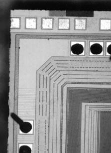
51 BIT LINE BIT LINE metal 2 GND V CC metal 1 WORD LINES polycide Figure 37. Topological SEM views of the Cache array. Mag. 5000x, 0.


52 BIT LINE BIT LINE metal 2 V CC GND metal 1 WORD LINES polycide Figure 38. Perspective SEM views of the Cache array. Mag. 6500x, 60.


53 GND V CC metal 1 WORD LINE V CC polycide Figure 39. Perspective SEM details of Cache SRAM cells. Mag. 13,000x, 60.


54 BIT BIT metal 2 BIT GND V CC BIT metal 1 Figure 40. Topological SEM views of Cache SRAM cells. Mag. 10,000x, 0.

55 1 GND 6 4 V CC 2 5 GND 3 polycide WORD 3 4 BIT 1 2 BIT 5 6 Figure 40a. Topological SEM view of Cache SRAM cells along with the cell schematic. Mag. 10,000x, 0.