Growth of Intermetallic Compounds during Isothermal Annealing of a Sn-Ag-Cu Lead-free Solder
|
|
|
- Theresa Greene
- 5 years ago
- Views:
Transcription
1 Accepted for publication in Soldering & Surface Mount Technology, Emerald, United Kingdom, 2004, in press. Growth of Intermetallic Compounds during Isothermal Annealing of a Sn-Ag-Cu Lead-free Solder S.L. Ngoh, W. Zhou, H. L. Pang and X.Q. Shi (c) School of Mechanical & Production Engineering, Nanyang Technological University, 50 Nanyang Avenue, Singapore (c) Singapore Institute of Manufacturing Technology, 71 Nanyang Drive Singapore Author for correspondence: Tel: ; Fax: ; WZhou@Cantab.Net Abstract Research and development of lead-free solders has been accelerated by impending WEEE and RoHS legislative ban on lead (Pb) in electronic products by 1 st July Considerable research has been carried out on Sn-Ag-Cu lead-free solders, because it is generally noted that Sn-Ag-Cu solders possess mechanical properties better than those of conventional Pb-Sn solders. However, formation of complex intermetallic compound (IMC) layers may have detrimental effects during prolonged thermal aging in service. Therefore, the primary objective of the study was to characterize the effects of isothermal thermal aging on the formation of IMC in the solder, with special attention paid to the interface between the solder and Cu with Ni/Au plating. Controlled experiment was conducted to study the effect of aging temperature and time on the microstructures coarsening. One hour annealing at 60 C and 125 C was observed to produce no discernable change in the microstructure. However, annealing temperature at 190 C resulted in coarsening of microstructure over time. Intermetallic growth measurement for Sn-Ag-Cu of lap shear solder/copper joint specimen subjected to isothermal aging at 125 C, 150 C, and 175 C over 24, 72, 144 and 336 hours were also studied. Increase in either isothermal aging time or temperature led to an increase in large elongated and platelet Cu 6 Sn 5 IMCs and ripening of interface (Cu,Ni)-Sn IMC layer. The growth of the interface IMC layer subjected to isothermal aging exhibits a linear relationship with respect to square root of aging time. 1. Introduction The implementation of lead-free solder manufacturing has become increasingly important in recent years due to legislation to ban lead (Pb) in electronic products by 1 st July 2006 in Europe. The NEMI organization recommends Sn95.5-Ag3.9-Cu0.6 (±0.2%) as the lead-free alloy candidate to replace 63Sn-37Pb solder. The test samples used in this study employ bulk solder to small solder ball joint specimens. Annealing or aging process is often conducted prior to mechanical test to eliminate residual stress and to stabilize the microstructure of the solder specimen. However, the parameters sets for these processes especially the temperature and time are very different and there are no standards available. In order to have a better understanding on these two annealing parameters on the microstructure evolution of the Sn-Ag-Cu lead-free solder, annealing experiments were carried out. Several studies [1-5] have reported that mechanical properties such as yield strength, tensile strength, creep-rupture and creep at elevated temperature of Sn-Ag-Cu lead-free solder are superior to 63Sn-37Pb solder. Electronic components are soldered to copper pad or terminal and are often plated with Ni surface finish and coated with immersion Au to give a diffusion barrier layer and oxidation protection layer. An IMC layer will be formed between tin in the molten solder and the surface finish layer and base metal during the reflow process. The melting adhesion is realized through this metallurgical bond and interfaced reaction. Solid state thermal diffusion causes the IMC layers to grow at an elevated temperature. Excessive growth of the IMC layer can deteriorate the solder joints reliability. In service, solder joints in an electronic assembly often fail by cyclic thermal loading. The failure is caused by thermal mismatch deformations resulting from differences in coefficient of thermal expansion of different electronic materials. In addition, thermally activated diffusion in the solder material, metallization and IMC take place during thermal cycling [6-9]. Understanding thermal aging degradation of the solder joint-to-pad interface behaviour in electronic assemblies is a critical concern in solder joint reliability. Therefore, it is important to study the kinetics of IMC thickening process using the solder/copper joint to simulate the solder joint in packing during growth process. A solder/copper joint specimen was employed for this study subjected to isothermal aging. 1
2 2. Experimental procedures 2.1 Annealing on bulk solder The 95.5Sn-3.8Ag-0.7Cu lead-free solder is supplied in cast-extruded bars and was sectioned into blocks with dimension of 25 mm x 15 mm x 15 mm. The melting temperature of the solder is about 217 C. The blocks were subjected to 1 hour annealing at 60 C (0.68 Tm), 125 C (0.81 Tm) and 190 C (0.94 Tm) respectively in a Lenton WHT4/30 oven to study the effect of annealing temperature on the microstructure in bulk solder. Another set of samples were subjected to varying exposure timing, 4, 9, 16 and 25 hours of annealing at 190 C, to study the effect of annealing time on the microstructure evolution. The microstructures of the specimen was observed in both the longitudinal and transverse direction as indicated in Figure 1. The specimens were moulded in an epoxy resin, ground, and finally polished using alumina suspension down to 0.3 µm followed by 0.06 µm of colloidal silica to achieve better surface finish. To reveal the microstructures, the polished specimens were etched slightly using an etchant with 5 vol% HCL in methanol for 5 to 15 seconds. The microstructure for the specimen in both the transverse and longitudinal directions were examined by optical microscope. Microstructure in longitudinal direction Extruded direction y z x Microstructure in transverse direction Figure 1 Sectioning of cast-extruded solder bar for microstructure preparation 2.2 Isothermal aging on solder/copper joint specimen Solder/copper joint specimens were fabricated by soldering two pieces of L shaped copper pieces. The surface finish is coated with about 3 µm nickel layer by electroless plating and about 0.05 µm finish of gold. The solder paste used is 95.8Sn3.5Ag0.7Cu no-clean solder paste. The solder/copper joint specimen is shown in Figure 2. The specimens were reflowed in a reflow oven with the heating profile as shown in Figure 3. The solder/copper joint specimens were subjected to isothermal aging using oven at 125 C, 150 C and 175 C for 1 (24 hrs), 3 (72 hrs), 6 (144 hrs) and 14 days (336 hrs) individually. When the isothermal aging reached the predetermine time, the specimen was air cooled in ambient condition at 23 C. For metallographic preparation, the specimens were mounted in an epoxy resin and were prepared for microstructure observation at the cross section at the joining part of the solder/copper joint specimen. The mounted solder/copper joint specimens were ground, polished and finally etched as per the bulk solder specimen. The microstructure was evaluated using JEOL JSM 6340F Field Emission Scanning Electron Microscopy (FE-SEM) and the composition of each phase was investigated by Energy Dispersive X-ray (EDX) microprobe analysis. The average height of interface IMC was determined using digital imaging techniques. In this method, the edges of the interface IMC were first outlined manually using the tracing tool. The average height of interface IMC was calculated by divided the area of IMC layer by the length in projected x direction as shown in Figure 4. 2


3 1.00 mm mm 7.00 mm 1.00 mm 2.00 mm 2.00 mm 2.20 mm mm Figure 2 Solder/copper joint testing specimen plan view and side view Solder Shaded area for IMC layer Peak Temp: 247ºC Total Time Above 217ºC: 116 s Figure 3 Reflow profile of the solder/copper joint specimen with peak temperature of about 250 C Length in projected x direction Copper sheet & coating layer Figure 4 Digital imaging techniques to determine the average IMC height 3


4 3. Results and discussion 3.1 Effect of annealing temperature and time on bulk solder The microstructure of the sectioned cast-extruded bar was observed in both longitudinal and transverse directions, as shown in Figure 1. The extruded direction of the solder bar is parallel to the x-axis of the optical micrograph in longitudinal direction, while for the optical micrograph in transverse direction is perpendicular to the paper plane. The representative microstructure of the cast-extruded solder bar in both longitudinal and transverse directions for the as-received condition are shown in Figure 5. The orientation of rod-like IMC was observed to follow the extruded direction. They are distributed in random orientation in the transverse direction as shown in Figure 5. Other than the rod-like IMC, small IMC particles were also observed. Some of the IMC in small particles form could be the cross-section view of the rod-like IMC. Rod-like IMC IMC particles Figure 5 Optical micrograph of the initial microstructure of the as-received cast-extruded solder bar in longitudinal showing rod-like IMC and IMC particles in Sn-matrix transverse directions showing disperse IMC particles. Annealing was performed on the cast-extruded solder bar to investigate the evolution of microstructures at different homologous temperature (T h ) levels and at various annealing times. Figures 6, 7 and 8 show typical optical micrographs of the cast-extruded solder bar after an hour of annealing at 60 C, 125 C and 190 C corresponding to about 0.68, 0.81 and 0.94 to the melting point of 490 K. In the cases of annealing temperatures at 60 C (Figure 6), no significant difference in the resultant microstructures in both longitudinal and transverse directions, when compared to the as-received condition (Figure 7). However for the annealing temperature at 190 C (Figure 8), the rod-like IMC were observed to be more rounded in shape and more randomly distributed. Since the impact of annealing temperature of 190 C on the microstructure is significant, the annealing process at the same temperature for 2 2, 3 2, 4 2 and 5 2 hours were performed. The study showed that the IMC structures were larger in size but smaller in number for longer annealing time. This can be seen by comparing the microstructure of the specimen annealed at 190 C for 1 hr in longitudinal direction (as shown in Figure 8 ) with those that annealed at the same temperature but longer duration as shown in Figure 9. However, the evolution of microstructure was found to be stabilized after 9 hrs of annealing at 190 C. There were no significant difference between the microstructures of the specimens that annealed for 9, 16 and 25 hrs at 190 C. 4


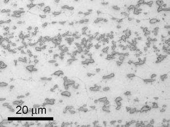
5 Figure 6 Optical micrograph of the cast-extruded solder bar after 1 hr of annealing at 60 C in longitudinal and transverse directions Figure 7 Optical micrograph of the cast-extruded solder bar after 1 hr of annealing at 125 C in longitudinal and transverse directions 190 C for 1 hrs Figure 8 Optical micrograph of the cast-extruded solder bar after 1 hr of annealing at 190 C in longitudinal and transverse directions showing more rounded IMC in random distribution. 5


![Research work on the similar reaction couple without subjected to any aging condition, such as, Ho [10], has reported that for Sn-Ag-Cu with the Ag concentration fixed at 3.](/docs-images/85/92084820/images/6-2.jpg "9wt% and Cu concentrations ranged from 0.6 to 3.0 wt%, (Cu 1-x Cu x ) 3 Sn 4 was not detected, but (Ni 1-y Ni y ) 6 Sn 5 layer formed between nickel and solder interface.")
![The same phase was observed by Zribi [11] on both Sn-Ag-Cu bulk and package samples with similar composition after reflow.](/docs-images/85/92084820/images/6-3.jpg "Therefore, it will be reasonable to report the Cu-Ni-Sn IMC that found at the solder/coating interface on this initial microstructure, as the (Ni,Cu) 6 Sn 5 IMC.")
6 190 C for 4 hrs 190 C for 9 hrs Figure 9 Optical micrograph of the cast-extruded solder bar annealed at 190 C for 4 hrs 9 hrs in longitudinal directions 3.2 Effect of isothermal aging on solder/copper joint The microstructures at the solder/coating interface for the solder/copper joint was examined. The initial microstructure of the as-reflow solder/copper joint specimen is shown in Figure 10. The EDX results show that the Cu-Ni-Sn needle-like of IMC layer was formed at the interface between solder/coating. Research work on the similar reaction couple without subjected to any aging condition, such as, Ho [10], has reported that for Sn-Ag-Cu with the Ag concentration fixed at 3.9wt% and Cu concentrations ranged from 0.6 to 3.0 wt%, (Cu 1-x Cu x ) 3 Sn 4 was not detected, but (Ni 1-y Ni y ) 6 Sn 5 layer formed between nickel and solder interface. The same phase was observed by Zribi [11] on both Sn-Ag-Cu bulk and package samples with similar composition after reflow. Therefore, it will be reasonable to report the Cu-Ni-Sn IMC that found at the solder/coating interface on this initial microstructure, as the (Ni,Cu) 6 Sn 5 IMC. As reflow Interface IMC ((Cu-Ni)-Sn) Solder Copper sheet Figure 10 SEM images and EDX results at interface of solder/copper joint specimen after reflow A series of SEM images of microstructure at solder interface of the solder/copper joint specimens exposured to isothermal aging at 125 C for different durations were presented in Figure 11. The (Cu-Ni)-Sn IMC in the form of needle-like structure was observed at the interface between solder/coating. The morphology is similar to that found in the initial microstructure, but its composition may have altered after isothermal aging exposure. The research work by Zribi [11] on the IMC evolution at the 95.5Sn3.5Ag1.0Cu/Ni interface shows that (Ni,Cu) 3 Sn 4 layer was formed between the (Ni,Cu) 6 Sn 5 /nickel interface after 16 hours aging at 150 C. True, existing isothermal aging temperature is lower at 125 C, the longer exposure time could have sufficient to cause the formation of (Ni,Cu) 3 Sn 4 layer. Based on the EDX analysis results as shown in Figure 12 and the possibility for the formation of both (Ni,Cu) 3 Sn 4 and (Ni,Cu) 6 Sn 5 interface IMC layers, the interface IMC layer found will be reported as (Ni,Cu)-Sn IMC. There were no distinct differences in the IMC layer between the specimens that subjected to various exposure periods at 125 C. In contrast, the interface (Cu-Ni)-Sn IMC layer was found to change from needle-like morphology to scallop-like shape with increasing isothermal aging time at higher aging temperature at 150 C and 175 C. The scallop-like morphology became more planer scallop-like shape after aged at 150 C and 175 C for 336 and 72 hours respectively. 6
 144 hrs (d) 336 hrs The height of the interface IMC layer was measured after reflow and exposure to isothermal aging at 125 C, 150 C and 175 C for 24, 72, 144 and")

 where D is the diffusion coefficient and t is the aging time.")

7 24 hrs at 125 C 72 hrs at 125 C 144 hrs at 125 C 336 hrs at 125 C (c) (d) Figure 11 Representative SEM images at solder/coating interface of the solder/copper joint speciment subjected to isothermal aging at 125 C for 24 hrs 72 hrs (c) 144 hrs (d) 336 hrs The height of the interface IMC layer was measured after reflow and exposure to isothermal aging at 125 C, 150 C and 175 C for 24, 72, 144 and 336 hours. The average height of the (Ni,Cu) 6 Sn 5 IMC formed after reflow was about 2.35 µm. As it was reported [12-14] that the atomic diffusion of Cu and Sn through the interface IMC layer is the mainly controlling process for the growth of the interface IMC during aging. The growth process that controlled by volume diffusion or by stationary grain boundary diffusion indicates that the growth kinetic of the interface IMC layer follow the square root time law, as expressed in equation below h = Dt (1) where D is the diffusion coefficient and t is the aging time. The diffusion coefficient is given by an Arrhenius expression, D= D 0 exp( Q/kT) (2) where D 0 is the diffusion constant, Q is the activation energy, k is the Boltzman constant and T is the absolute temperature. The interface IMC growth trend as shown in Figure 13 was presented by plotting the average height with respected to square root of aging time up to 144 hrs. The plot shows that the growth of the (Ni,Cu)-Sn IMC displays a nearly linear relationship to square root of aging time. By comparing the initial growth rate of the interface (Ni,Cu)-Sn IMC layer subjected to isothermal aging at different temperature levels as shown in Figure 13, it was found that the aging temperature at 125 C is not high enough to cause any significant growth. Isothermal aging at 150 C and 170 C exhibited the growing rate of about 7 and 14 times faster than that at 125 C respectively. 7
 6.0 5.0 4.0 3.0 2.0 1.0 0.")
8 Solder Interface IMC (Cu,Ni)-Sn Copper sheet Figure 12 The representative EDX analysis on the IMC layer at the solder/coating interface of the solder/copper specimen after subjected to 150 C for 144 hours Avearge height (µm) C 150 C C Square root of aging time (hr)1/2 Figure 13 Growth of interface IMC compound with respect to square root of isothermal aging time 4. Conclusions Effect of temperature on the solder microstructure was studied using a fixed annealing time of 1 hour but various annealing temperatures ranging from 60 C to 190 C. Annealing at 60 C or 125 C produces no observable change in the microstructure. However, higher annealing temperature of 190 C results in IMCs which are smaller in number, larger in size and more rounded in shape, indicating the growth of large IMCs at the expense of the small ones. Effect of time on the microstructures was studied for a fixed high annealing temperature of 190 C. It is found that increasing the time from 1 hour to 9 hours leads to coarsening of the IMCs. The evolution of microstructure was stabilized after 9 hours of annealing at 190 C as no significant coarsening of IMC can be observed. Growth interface IMC was not significant for isothermal aging at 125 C. This was corresponded to the results obtained from the study of annealing temperature on cast-extruded bar which showed that annealing temperature at 125 C was not high enough to cause any significant change in microstructure. However, interface IMC growth was prodigious for higher temperature at 150 C and 175 C. The growth of the interface IMC was initially linearly proportional to square root of aging time up to 144 hours but was levelled off with longer aging time for 336 hours. These phenomenon was suggested to be caused by the limited supply of Ni for (Cu,Ni)-Sn intermetallic compound formation, and its growing rate in z-direction was marked by the ripening process of (Cu,Ni)-Sn phase in multiple directions. 8
9 References [1]. Plumbridge, W.J., C.R. Gagg, and S. Peters (2001) "The creep of lead-free solders at elevated temperatures", Journal of Electronic Materials, vol. 30, no. 9, pp [2]. Wade, N., et al. (2001) "Effects of Cu, Ag and Sb on the creep-rupture strength of lead-free solder alloys", Journal of Electronic Materials, vol. 30, no. 9, pp [3]. Mutoh, Y., et al. (2002) "Fatigue crack growth behaviour of lead-containing and lead-free solders", Soldering & Surface Mount Technology, vol. 14, no. 3, pp [4]. Kim, K.S., S.H. Huh, and K. Suganuma (2002) "Effects of cooling speed on microstructure and tensile properties of Sn-Ag-Cu alloys", Materials Science and Engineering A, vol. 333, no. 1-2, pp [5]. Pang, H.L.J., et al. (2001) "Microstructure and intermetallic growth effects on shear and fatigue strength of solder joints subjected to thermal cycling aging", Materials Science and Engineering A, vol. 307, no. 1-2, pp [6]. Zhang, C., J.-K. Lin, and L. Li (2001), "Thermal fatigue properties of lead-free solders on Cu and NiP under bump metallurgies", Proceedings of 51 st Electronic Components and Technology Conference, May - June 2001, Orlando, Florida, USA, pp [7]. Ma, X., Y. Qian, and F. Yoshida (2002) "Effect of La on the Cu-Sn intermetallic compound (IMC) growth and solder joint reliability", Journal of Alloys and Compounds, vol. 334, no. 1-2, pp [8]. Zeng, K. and K.N. Tu (2002) "Six cases of reliability study of Pb-free solder joints in electronic packaging technology", Materials Science and Engineering R, vol. 38, no. 2, pp [9]. Pang, J.H.L., et al. (2004) "Intermetallic Growth Studies on Sn-Ag-Cu Lead-Free Solder Joints", Journal of Electronic Materials. [10]. Ho, C.E., et al. (2002) "Effect of Cu concentration on the reactions between Sn-Ag-Cu solder and Ni", Journal of Electronic Materials, vol. 31, no. 6, pp [11]. Zribi, A., et al. (2001) "The growth of intermetallic compounds at Sn-Ag-Cu solder/cu and Sn-Ag-Cu/Ni interfaces and the associated evoluation of the solder microstructure", Journal of Electronic Materials, vol. 30, no. 6, pp [12]. Guan, Z.M., G.X. Liu, and T. Liu (2000) "Kinetics of interface reaction in 40Sn-Bi/Cu and 40Sn-Bi- 2Ag/Cu systems during aging in solid state", IEEE Transactions on Advanced Packaging, vol. 23, no. 4, pp [13]. Xiao, G.-W., et al. (2001) "Effect of Cu stud microstructure and electroplating process on intermetallic compunds growth and reliability of flip-chip solder bump", IEEE Transactions on Advanced Packaging, vol. 24, no. 4, pp [14]. Young, C.C., J.G. Duh, and S.Y. Tsai (2001) "Microstructural evolution in the Sn-Cu-Ni and Pb-Sn Solder Joints with Cu and Pt-Ag metallized Al 2 O 3 substrate", Journal of Electronic Materials, vol. 30, no. 9, pp