MEMS Packaging Techniques for Silicon Optical Benches
|
|
|
- Molly Holmes
- 5 years ago
- Views:
Transcription
1 MEMS Packaging Techniques for Silicon Optical Benches Hayden Taylor David Moore, Mohamed Boutchich, Billy Boyle, Johnny He, Graham McShane, Richard Breen, Rob Wylie CAMBRIDGE UNIVERSITY ENGINEERING DEPARTMENT 3 March 2004

2 Introduction Why MEMS for optoelectronic packaging? high precision required: ±0.5 micron, ±0.7 towards parallel assembly avoid expense of nanomanipulator optical demultiplexer cross-section Lens/filter/mirror/prism/diode Fibre Fibre glue Microclip
3 Introduction Why rapid prototyping? many new materials mechanical design hard

4 Introduction Why rapid prototyping? many new materials mechanical design hard Laser beam 3ns 50Hz 0.6mJ/pulse 355nm or 532nm 50μm-diameter spot y x sample (moves) New Wave


5 Introduction Why rapid prototyping? many new materials mechanical design hard substrate parasitic undercut Laser beam 3ns 50Hz 0.6mJ/pulse 355nm or 532nm 50μm-diameter spot y x sample (moves) A A SiN x cantilever A A plan section


6 Introduction Previous MEMS packaging work: passive Cross-section SEM Journal Micromechanics Microengineering 8, (1998)
 mems.")
7 Introduction Previous MEMS packaging work: out of plane polysilicon multi-layer processes (e.g. SUMMiT, Sandia) mems.sandia.gov
 surface tension: self-assembly self-assembled inductor Heat solder Imperial College http://www.")
8 Introduction Previous MEMS packaging work: out of plane polysilicon multi-layer processes (e.g. SUMMiT, Sandia) surface tension: self-assembly self-assembled inductor Heat solder Imperial College
9 Outline Laser micromachining: characterisation Extracting mechanical properties Analysis + concepts Silicon-on-insulator clamps: bistable, thermal Thin film microclips Inflatable MEMS substrate hinged SOI bistable clamp thermal bimorphs component rubber film substrate applied pressure
10 Outline Laser micromachining: characterisation Extracting mechanical properties Analysis + concepts Silicon-on-insulator clamps: bistable, thermal Thin film microclips Inflatable MEMS


11 Characterising laser ablation of silicon nitride 3ns-pulse 3.5eV (UV), 50Hz, 10μms mm 3ns-pulse 2.3eV (Green), 50Hz, 10μms mm 3ps-pulse 1.2eV (IR), 50kHz, 10mms -1 Lumera Laser 0.1mm
12 Characterising laser ablation of silicon nitride SiN (2μm) SiN (0.2μm) ta-c(0.1μm) Bare silicon threshold
13 Characterising laser ablation of silicon nitride
14 Characterising laser ablation of silicon nitride 2 μm
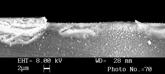

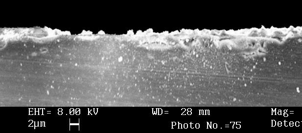
15 Characterising laser ablation of silicon nitride 2 μm
16 Characterising laser ablation of silicon nitride Optical micrograph


17 Characterising laser ablation of silicon nitride Optical micrograph sample surface Film thickness = 2μm Profilometer trace


18 Characterising laser ablation of silicon nitride Use ablation to create shallow microfluidic channels?
19 Outline Laser micromachining: characterisation Extracting mechanical properties Analysis + concepts Silicon-on-insulator clamps: bistable, thermal Thin film microclips Inflatable MEMS
20 Extracting Young s Modulus of thin films resonance frequency measurement 1 electrostatic pull-in 2 microbeam deflection with nanoindenter 3 [1] M Madou: Fundamentals of Microfabrication, p270 [2] Journal MEMS, pp [3] WD Nix: Measurement of Mechanical Properties in Small Dimensions by Microbeam Deflection, Stanford

![M Madou: Fundamentals of Microfabrication, p270 [2] Journal MEMS, 6 2 1997 pp107 118 [3] WD](/docs-images/85/92719648/images/21-1.jpg "Nix: Measurement of Mechanical Properties in Small Dimensions by Microbeam Deflection,")
21 Extracting Young s Modulus of thin films resonance frequency measurement 1 electrostatic pull-in 2 microbeam deflection with nanoindenter 3 scanning profilometer along microbeam [1] M Madou: Fundamentals of Microfabrication, p270 [2] Journal MEMS, pp [3] WD Nix: Measurement of Mechanical Properties in Small Dimensions by Microbeam Deflection, Stanford
22 bow tilt Extracting Young s Modulus of thin films I u F(x) E, ν x 0 L u L x I z = F{(x-x 0 -L u ) 3 /3EI + (x-x 0 -L u ) 2 L u /EI u + (x-x 0 -L u )L u2 /EI u + L u3 /3EI u )} = Fx 3 /3EI + O(x 2 )
L u2 /EI u + L u3 /3EI u )} = Fx 3 /3EI + O(x 2 ) Vertical deflection, z 0 Fitting range distance along")
23 bow tilt Extracting Young s Modulus of thin films I u F(x) E, ν x 0 L u L x I z = F{(x-x 0 -L u ) 3 /3EI + (x-x 0 -L u ) 2 L u /EI u + (x-x 0 -L u )L u2 /EI u + L u3 /3EI u )} = Fx 3 /3EI + O(x 2 ) Vertical deflection, z 0 Fitting range distance along beam
24 Extracting Young s Modulus of thin films additional problems anticlastic curvature affects effective stiffness stylus force varies with deflection local indentation beam twisting


25 Extracting maximum stress of thin films A A A A
26 Outline Laser micromachining: characterisation Extracting mechanical properties Analysis + concepts Silicon-on-insulator clamps: bistable, thermal Thin film microclips Inflatable MEMS
27 Problem abstraction
28 Specification 1. Alignment precision: 0.1dB coupling loss requires 0.5µm and 0.7 but throw must be larger 2. Components to be held sub-millimetre: lenses, mirrors and fibres 3. Slop: component dimension tolerances up to 10% 4. Up to 2 linear and 3 angular degrees of freedom or vice versa 5. Power and area budgets: debatable
29 Outline Laser micromachining: characterisation Extracting mechanical properties Analysis + concepts Silicon-on-insulator clamps: bistable, thermal Thin film microclips Inflatable MEMS hinged SOI substrate bistable clamp
30 DRIE structure Lens manipulator

31 DRIE structure Lens manipulator


32 Out-of-plane bistable clamps θ 1 N Pa 500 μm F θ 1 Passes: θ 1 Laserthinned hinges 60-micron SOI base SEM cross-section of SOI thinning experiment
33 Outline Laser micromachining: characterisation Extracting mechanical properties Analysis + concepts Silicon-on-insulator clamps: bistable, thermal Thin film microclips component Inflatable MEMS thermal bimorphs
34 Proposed microclips When a component is inserted, the microcantilevers deflect and hold the component in static equilibrium. Fabrication 1. deposit thin film on to wafer 2. photolithography or laser micromachining to define cantilevers 3. anisotropic etch through wafer
35 Proposed microclips When a component is inserted, the microcantilevers deflect and hold the component in static equilibrium. Fabrication 1. deposit thin film on to wafer 2. photolithography or laser micromachining to define cantilevers 3. anisotropic etch through wafer V-groove Si substrate Pyramidal pit Elastic fixture Fibre Ball lens Filter/ mirror
36 Deflection of Microbeams A thin beam subject to a tip displacement constraint assumes a shape that minimises energy. To obtain a minimum energy state we must vary the shape function of the cantilever until the integral energy function reaches a stationary point. Shape that minimises stored energy L dy E = k F( y,, xdx ) dx 0 Etot = Mκ ds Discretisation The integral expression can be approximated by a series expression. The system effectively becomes a series of rigid members joined by torsional springs whose spring constant gives the same bending rigidity per unit length as the continuous bar. n-1 [U n-1, V n-1 ] E tot n= 0 2 θ n-1 Δs N EI = Δ Δs θ n [U n, V n ] 2 n θ n Δs n+1

 Subject to constraints Tip Displacement + segment angle IEEE 2002 Electronics")
37 Deflection of Microbeams Excel contains an optimisation plug-in called Solver. This allows us to Minimise an objective function Stored Energy By changing a set of variables Bar Angles (θ 0...θ n ) Subject to constraints Tip Displacement + segment angle IEEE 2002 Electronics Components and Technology Conference, San Diego, U.S.A., s19p3, pp. 1-7 (2002)
38 Processing variations and probabilistic design For optical benches components must be precisely aligned in the vertical plane. Process variability can lead to component misalignment. Lithographic error Deposition variation Front-Back Misalignment Component tolerances Vertical Alignment of Component Energy Investigate the effect of each error and build a distribution of vertical alignment. Force Clearance/clip length
39 Processing variations and probabilistic design within specification 120% 100% Frequency % 60% 40% 20% Misalignment Angle 0%
40 Towards active clips cold 1 2 Thicknesses a 1, a 2 Thermal expansivities are α 1, α 2 Moduli E 1, E 2 Increase in temperature ΔT E 1 /E 2 = n a 1 + a 2 = t a 1 /a 2 = m K = 6(1 + m) 2 / [3(1 + m) 2 + (1 + mn)(m 2 + 1/mn)] hot Thermal curvature is given by: κ = K(α 2 α 1 )ΔT/t
41 Extending energy simulation to 4 thermal clips mm No misalignments
42 Extending energy simulation to 4 thermal clips mm Total elastic energy ψ A x B B B A ψ No misalignments Local energy minimum with antisymmetric clip orientations rotation ψ = 11.5
43 Extending energy simulation to 4 thermal clips mm ψ x μm No misalignments μm front-to-back misalignment rotation ψ = 2.1 x 0
44 Extending energy simulation to 4 thermal clips mm ψ x μm No misalignments μm front-to-back misalignment rotation ψ = 2.1 x countered by 20K temp increase in red clip. (150nm Ni/SiN x ) rotation ψ = 0.4 x 0
45 Extending energy simulation to 4 thermal clips mm ψ x No misalignments K temperature increase in clips 1 and 2 rotation ψ ~ 2 x ~ 5 μm
46 Outline Laser micromachining: characterisation Extracting mechanical properties Analysis + concepts Silicon-on-insulator clamps: bistable, thermal Thin film microclips Inflatable MEMS rubber film substrate applied pressure

47 Why consider inflatable MEMS? sharp edges unstressed films in tension mean larger holding forces inherent damping fluid could solidify
48 Conclusions Laser micromachining cutting slow / refinement fast material damage can probably be controlled UV/silicon nitride combination ideal Modulus extraction target accuracy better than 20% noise in data remains largest problem Deep reactive ion etching + strong + well-characterised large footprint Thin-film microclips + simple + compact max. stress high Inflatable MEMS + manipulate and fix in one step + strength from inflation not high modulus unproven