Nanoparticle generation using sputtering plasmas
|
|
|
- Gyles Armstrong
- 5 years ago
- Views:
Transcription


1 NCCAVS Joint Users Group Technical Symposium Nanomaterials for Energy, Biomedical, and Electronic Devices In Conjunction with the NCCAVS 35th Annual Equipment Exhibition Nanoparticle generation using sputtering plasmas André Anders * and César Clavero Plasma Applications Group Lawrence Berkeley National Laboratory *Presenter. aanders@lbl.gov February 20,


2 synthesis & materials plasmas characterization


3 HiPIMS an important theme for some years. Moving Ionization Zones Nb discharge, peak ~ 200 A reduction of image exposure time gives immediate clues on rotational speed ~ 10 4 m/s A. Anders et al., J. Appl. Phys. 111 (2012)

4 Streak image sequence, 20 µs sweep time z, (mm) A. Anders et al., J. Appl. Phys. 111 (2012)

 J. Priestley, The History and Present State of Electricity, 3rd ed., London, 1775; A. Anders, IEEE Trans. Plasma Sci.")
5 Perhaps the first observation of nanoparticles The black dust was so extremely light as to rise like a cloud in the air, so as sometimes to be visible near the top of the room; I concluded that it could not be the metal itself, but probably the calx [oxide],.i was confirmed in this opinion by finding that this black dust collected from a brass chain would not conduct electricity (J. Priestley, 1775) J. Priestley, The History and Present State of Electricity, 3rd ed., London, 1775; A. Anders, IEEE Trans. Plasma Sci. 31 (2003)


 ZnO:Al (AZO) SnO 2 :F (FTO) ZnO:Ga (GZO) Other")
 at 68 C")
6 Starting Point: Plasma-Assisted Deposition of Oxide Films R. J. Mendelsberg, et al., J. Physics D 44 (2011) AZO, 605 nm, 18 Ω/ ITO, 140 nm, 7.9 Ω/ Interesting for energy related applications: Transparent in visible and near infrared ranges High electrical conductivity Solar spectrum In :Sn0 2 (ITO) ZnO:Al (AZO) SnO 2 :F (FTO) ZnO:Ga (GZO) Other metal oxides of interest: VO 2 : thermochromic material: Metal-to-insulator transition (MIT) at 68 C TiO 2 : Wide band-gap semiconductor, catalysis applications WO 3 : electrochromic material 6


7 From Films to Nanoparticles and Nanocomposites Localized Surface Plasmon Resonance Electric field Resonance: frequency of field is equal to plasma frequency of free electrons Resonance is size-dependent 7
8 Metal vs. TCO Nanoparticles as Plasmonic Materials Extintion (arb. units) Al Ag Au Cu RuO 2 AZO increasing concentration of carriers n=0.5-10x10 20 cm -3 ITO Wavelength (nm) Solar Spectral Irradiance AM1.5 (W m -2 nm -1 )

")


9 Some Applications of Nanostructured Oxides Smart Windows Solar heat (infrared radiation) Visible light Ultimate Goal: independent switching in the visible and infrared ranges Photovoltaic and Photocatalytic devices H. A. Atwater and A. Polman, Nat. Mater. 9 (2010)

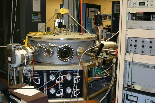
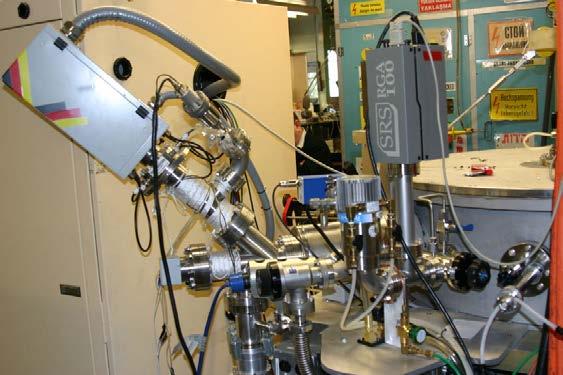
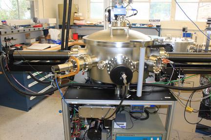
10 Approach: Terminated Cluster Growth Source: Mantis Deposition LTD 10

11 Terminated Cluster Growth Setup Nanoparticle generator integrated in a sputtering process chamber: option to combine nanoparticles and thin film in devices 11
12 Nanoparticle Generator video Source: Mantis Deposition LTD 12
13 Effect of Density of Nucleation and Growth Number of nanoparticles (arb. units) Vanadium target The nanocrystals size and production rate can be varied by controlling a number of parameters including: Sputtering gas flow rate Aggregation zone pressure Position of the target in the aggregation zone Sputtering power Increased collision rate increases number and size and nanoparticles. 13
 10 5 450 400 350 300 250 Voltage (V) 0 0.00 0.05 0.10 0.15 0.20 0.25 0.")
14 Effect of Argon and Oxygen Flows on Nanoparticle Formation Even very small amounts of oxygen affect the outcome greatly sccm 50 sccm 100 sccm 200 sccm Ar flow, p = mtorr in aggregation zone 500 average nanoparticle size (nm) Voltage (V) Oxygen flow (sccm) C. Clavero, et al., J. Phys. D: Appl. Phys. 46 (2013)
15 Effect of Oxygen on Nanoparticle Size and Rate nanoparticle flux (arb. units) Vanadium target, 50 sccm Ar flow (const.) sccm O sccm O sccm O sccm O sccm O sccm O sccm O Diameter (nm) target voltage (V) O 2 flow (sccm) heterogeneous nucleation is much more effective than homogenous nucleation there is a very pronounced parameter window of effective oxide nanoparticle formation C. Clavero, et al., J. Phys. D: Appl. Phys. 46 (2013)

 68 C VO 2")

16 Why Vanadium Oxide? Low temperature monoclinic phase (insulating) High temperature rutile phase (metallic) 68 C VO 2 is a thermochromic material VO 2 nanocrystals are difficult to synthesize by solution chemistry 16
17 Vanadium Oxide: Very Complicated Phase Diagram this is the desired phase C. H. Griffiths and H. K. Eastwood, J. Appl. Phys. 45, (1974)
18 RBS: Checking the Nanoparticle Composition 350 mtorr 1 Torr counts (arb. u.) O V counts (arb. u.) O V concentration Energy (kev) Energy (kev) O V VO 2 Substrate depth (10 15 at/cm 2 ) concentration V VO O Substrate depth (10 15 at/cm 2 ) C. Clavero, et al., J. Phys. D: Appl. Phys. 46 (2013)
 XRD VO 2 V 2 O 5 V 3 O 7 650 o C 550 o C 450 o C 400 o C 375 o C 350 o C 300 o C 250 o C RT 10 20 30 40 50 60 70 2Theta (deg) C. Clavero, et al., J. Phys.")
19 Control of Morphology and Crystal Structure by Annealing Grain size (nm) Temperature ( o C) Intensity (arb. units) XRD VO 2 V 2 O 5 V 3 O o C 550 o C 450 o C 400 o C 375 o C 350 o C 300 o C 250 o C RT Theta (deg) C. Clavero, et al., J. Phys. D: Appl. Phys. 46 (2013)
20 From Nanoparticles to Nanocrystals Optimum thermal treatment (375 C < T < 500 C) VO 2 nanocrystals As deposited (amorphous VO 2 ) After thermal treatment (crystalline VO 2 ) (011) I (arb. u.) (211) (210) (220) Theta (deg.) 2 Theta (deg.) C. Clavero, et al., J. Phys. D: Appl. Phys. 46 (2013)
21 Spectral Response: Demonstrate Switching temperature at measurement annealing temperature Wavelength (nm) Wavelength (nm) C. Clavero, et al., J. Phys. D: Appl. Phys. 46 (2013)
22 Spectral Response: Checking Change in Transmission greatest optical switching happens here T λ =T λ (25 o C) - T λ (90 o C) Annealing temperature ( o C) Wavelength (nm)
23 Hysteresis of the Transition Temperature as a Function of Annealing C. Clavero, et al., J. Phys. D: Appl. Phys. 46 (2013)

24 at λ= 1500 nm Hysteresis of Phase Transition

 for oxide nanoparticle synthesis 1. even little oxygen promotes heterogeneous nucleation 2.")
25 Summary & Conclusions 1. Oxide nanocrystals can have plasmonic properties; depend on free carrier concentration and size 2. Especially interesting are those that show insulator-tometal transition, such as thermochromic VO 2 3. Demonstrated Terminated Cluster Growth as a synthesis method for VO 2 nanoparticles 4. There is a pronounced optimum of oxygen partial pressure (flow) for oxide nanoparticle synthesis 1. even little oxygen promotes heterogeneous nucleation 2. too much oxygen poisons the target and reduces rate 5. Demonstrated transition from nanoparticles to nanocrystals with optimum annealing temperature ~ 400 C as judged by maximum switching in the infrared (1500 nm) 25
26 Outlook 1. Use pulse sputtering we have seen significant rate increases 2. Use in-situ annealing to obtain nanocrystals 3. Use multi-element targets and gases 4. Embed nanoparticles/crystals in a matrix and make devices 5. Scale to a linear system for large area