Summary of Selected EMCR732 Projects for Spring 2005 Mike Aquilino Dr. Lynn Fuller
|
|
|
- Corey Morton
- 5 years ago
- Views:
Transcription
1 ROCHESTER INSTITUTE OF TECHNOLOGY MICROELECTRONIC ENGINEERING Summary of Selected EMCR732 Projects for Spring 2005 Mike Aquilino Dr. Lynn Fuller Motorola Professor 82 Lomb Memorial Drive Rochester, NY Tel (585) Fax (585) Projects05.ppt Page 1
2 INTRODUCTION Each of the students in EMCR650 and EMCR732 are asked to do a process improvement project to make the student factory better. In place of a final exam they present their project results. Students in EMCR731 did a observational study of particulate contamination in some of the tools in the laboratory. This document is a summary of some of their presentations. Page 2
3 OUTLINE Introduction Thin Gate Oxide Growth by Rapid Thermal Processing (RTP) Measurement of 50Å Oxides at RIT Surface Charge Analyzer (SCA) Measurements of Oxide Quality New Aluminum Etch Recipe for Lam4600 with Endpoint Detection Rework Strategy for Aluminum Etch in Lam4600 Testing of First CMOS DAC Lot Four Levels per Mask Plate Stepper Job for Canon Stepper Drytek Quad Nitride Sidewall Spacer Etch Uniformity Simulation of Threshold Adjust Implant for Adv-CMOS Process Page 3

4 THIN GATE OXIDE GROWTH BY RAPID THERMAL PROCESSING (RTP) From Textbook by S. Wolf Textbooks say that 150Å of oxide can be grown by RTP at 1100 C in 60 sec. Page 4
5 RTP RECIPE Recipe for RTP Oxide, time during SS (Steady State) was changed to obtain different oxide thicknesses, 60s, 120s, 240s, and 480s Step Time (sec) Temp (C) T sw Gain Dgain Iwarm Icold Delay 10 Ramp SS SS Delay 300 Sébastien Michel, February 2005 Steve Parshall, Kazuya Tokunaga, May 2005 Page 5
6 OXIDE THICKNESS MEASUREMENTS The data shown was obtained using the 5 point 6 wafer Spectromap RTP Oxide at 1000 C, Dry O2 Time Mean Max Min STDDEV Center Pts Minutes A A A % A The data shown was obtained using the VASE (Variable Angle Spectroscopic Ellipsometer) Time Xox n Min A Page 6
7 OXIDE MEASUREMENTS COMPARISON Oxide Measurements Comparison Oxide Measurements (A) Time (minutes) V.A.S.E Spectromap Rudolph Ellipsometer Nanospec We believe the VASE and the Sprctromap are the best measurement tool for under 100 A Page 7
8 RTP OXIDE QUALITY MEASUREMENTS Measurements made using the SCA (Surface Charge Analyzer) Time 8 minutes 4 minutes 2 minutes 1 minute NSC 1.13E E E E+14 Qox 3.55E E E E+11 Dit 2.76E E E E+11 Qfb 4.66E E E E+11 Ts Dit is close to Bruce Furnace thermal gate oxide values Typically ~1E11 Page 8
9 UNIFORMITY OF SURFACE STATE DENSITY Experiments: 2 P-type bare wafers RCA clean TCA clean of the oxidation furnace, Bruce Tube 4. Gate oxide growth, 150A thin oxide growth, dry O2 Bruce recipe 215. Thickness measurement: 5 points, average value: 140A, standard deviation < 10A. Wafers inserted in the furnace show hundreds of added particles so did RCA clean without HF step. SCA 2500: Use Recipe FAC-P with a test wafer (known oxide thickness) in order to calibrate the probe by measuring 1 point. Program 9PTSQSIX, 9 points. 9 points square Wafer 1 Wafer 2 Sébastien Michel Spring Quarter 2005 T s (usec) Si doping (/cm3) N sc D it (traps/cm2/ev) 1,07e14 Std dev: 0,02e14 1,41e11 Std dev: 0,07e Std dev: 5 0,90e14 Std dev: 0,01e14 0,84e11 Std dev: 0,02e Std dev: 7 Page 9

10 ALUMINUM ETCH RECIPE END POINT DETECTION By Gianni Franceschinis Page 10
11 LAM 4600 Al Etcher Plasma Chemistry Cl2 Reduces Pure Aluminum BCl3 Etches native Aluminum Oxide -Increases Physical Sputtering N2 Diluent and carrier for the chemistry Chloroform Helps Anisotropy and reduces Photoresist damage Page 11
12 LAM 4600 Al Etch Film Stack Used: Sputtered Aluminum, CVC 601 5mTorr, 16 sccm Ar flow rate, 2000 watts 1500 Seconds (5 min pre sputter) Average Al Thickness 8400Å 5000Å Wet Oxide Bruce Furnace Tube 1, Recipe 50 Page 12
13 LAM 4600 Al Etch Recipe 12: Jeremiah Hebding Step Pressure (mtorr) RF Top (W) RF Bottom (W) Gap (cm) N BCl Cl Ar CFORM Complete Stabl Time endpoint Oetch time time (s) % 15 Never endpoints, always goes 120 seconds Page 13
14 LAM 4600 Al Etch Plot Configuration (Trend Menu) Name Mode Start End Target Input Sample Rate Start V.Slope Value Stop V.slope Value A 1 Manual Hard > 1 53 < 0 B 2 Manual Hard > 1 53 < 0 Page 14
15 LAM 4600 Al Etch Typical Endpoint signal Time (secs) Page 15
16 LAM 4600 Al Etch Final Proposed Recipe: Number Step Pressure (mtorr) RF Top (W) RF Bottom (W) Gap (cm) N BCl Cl Ar CFORM Complete Stabl Time endpoint Oetch time time (s) % 15 Gianni Franceschinis, May 2005 Rate ~50Å/s Channel B Delay 130 Normalize 10 s Norm Val 5670 Trigger 105% Slope + Page 16
17 LAM 4600 Al Etch Rework Strategy Aluminum Etch Rework Strategy: If the etch was not complete use the following procedure to do an additional etch 10 seconds Aluminum wet etch Spin Rinse Dry (SRD) LAM 4600 Recipe 12 or with manual endpoint calculated from 50Å/s etch rate Page 17

18 LAM 4600 Al Etch Conclusion: Endpoint detection is possible if the endpoint signal parameters are set appropriately A rework strategy was developed for incompletely etched wafers. Gianni Franceschinis, May 2005 Page 18


19 TESTING OF FIRST DAC LOT Page 19
20 2 µm NMOS TRANSISTOR Page 20

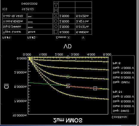
21 2 µm NMOS ID vs VGS Page 21
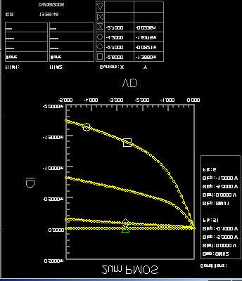
22 2 µm PMOS TRANSISTOR Page 22

23 PMOS TRANSISTOR ARRAY Page 23

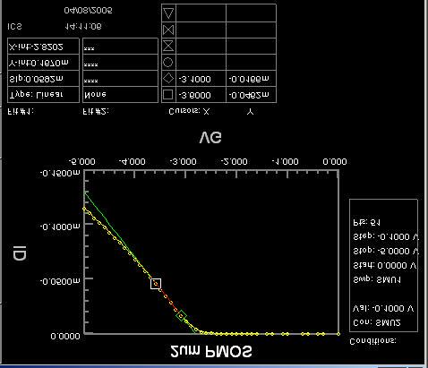
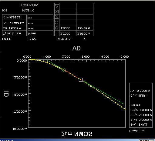
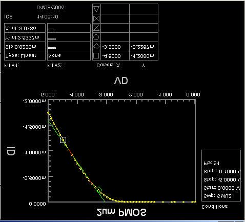
24 2 µm PMOS ID vs VGS Page 24

25 2µm INVERTER Page 25

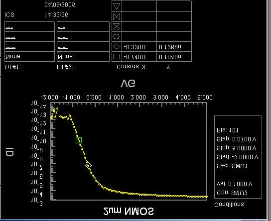
26 2 µm INVERTER Page 26

27 73 STAGE RING OSCILLATOR Page 27
28 CANON STEPPER JOBS FOR 4-LEVELS/RETICLE The objective of this project is to write stepper jobs for the Canon stepper that will allow the use of masks with four levels per quartz plate. The key things that need to be changed are the masking blade positions in the shot file and shifts in the layout file. Four mask layers are placed on a single mask by placing the center of each layer 20 mm x 20 mm from the center of the quartz plate. This corresponds to a 4 mm x 4 mm shift on the wafer. The shifts are +4,+4 and +4,-4 and 4,+4 and 4,-4 depending on which quadrant is being printed. The blade positions are also different depending on which quadrant is being printed. Page 28
29 CANON STEPPER JOBS FOR 4-LEVELS/RETICLE Robert Manley May 16, 2005 MIXED4X1 MASK SET Page 29
30 CANON STEPPER JOBS FOR 4-LEVELS/RETICLE We named the Stepper Jobs: Level 1: MIXED4X1_NWEL Level 2: MIXED4X1_ACT Level 3: MIXED4X1_STOP Level 4: MIXED4X1_VT BU + We named the Reticle File: RMIXED4X with the following reticle ID s and blade positions. BL - 0,0 + BR Level RMIXED4X1 BL -8 BR 8 BU 0 BD 0 - BD RMIXED4X2 RMIXED4X3 RMIXED4X Page 30
31 UNDERSTANDING THE PROBLEM If Shot with Blades Open Blade Position Normal Die Reference 4 Level Mask Die Reference 0,0 0,0 Page 31
32 UNDERSTANDING THE PROBLEM If same layout file is used Level 1 Level 2 Page 32
33 UNDERSTANDING THE PROBLEM Need to include a layout (block) shift of successive levels (not shot shifting) Duplicated the level 1 layout but include a layout shift Shift Level 2 Down Page 33

34 BLOCK SHIFTING Copy level 1 layout file Create Block and Shift Edit layout>create Block>Shift Block Page 34
35 LAYOUT SHIFTING Similar shifting is done for higher levels Because higher levels are shifted, need to add shift for TVPA mark locations in each level process file Page 35

36 RESULTS Currently alignment with TVPA marks is successful Work still needs to be completed with fine alignment marks Both Levels Aligned Page 36
37 CONCLUSION Successful alignment using TVPA marks has been accomplished using the 4x1 mask on the Canon Stepper Work is still in progress on how to incorporated the use of the fine alignment marks Robert Manley, May 16, 2005 Page 37


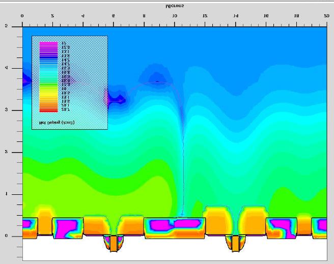
38 INVESTIGATION OF ETCH UNIFORMITY This project involved an investigation of the etch uniformity for the nitride sidewall spacer etch used in our advanced CMOS process. Swapnyl Shah, May 2005 Page 38
39 PROCEDURE 1. Standard factory recipe to grow 500A gate oxide using Bruce Oxide measurement using Standard 5 point measurement on the wafer showed uniform 500A oxide growth. 3. Followed by 3500A Nitride deposition using ASM LPCVD tool. 4. The thickness measurement and deposition rate distribution profile was analysed on Tencor Spectramap. Mean thickness of 3044A with std deviation of 204.7A was measured on 24 pre-selected points. 5. Nitride was etched using the Drytech Quad, Reactive Ion etching system with wafer on metal plate and later using a quartz plate beneath the wafer. Pressure was set to 50 mtorr. Recipe???? 6. Half of the nitride was etched using a pre-determined etch rate of 1100A/min for 1.5 min and later analyzed for uniformity on the Tencor Spectramap. Page 39
40 The wafer placed with flats up during the Nitride deposition. MEASUREMENTS Wafer placed with flats facing the user during etching nitride using the Drytech Quad. Wafer placed with flats aligned to the plate on Spectramap and measurement taken on the following points. Wafer positioning very important during each step of wafer processing. Page 40
41 DATA Wafer position vs etch rate Wafer position Vs Etch rate for wafer #1 on metal plate etch rate Series1 wafer Position Wafer position Vs Etch rate for wafer #2 on quartz plate Etch rate wafer position vs Etch rate Wafer Position wafer position vs Etch rate Page 41


42 SPECTROMAP RESULTS Wafer 1 after nitride dep Wafer 1 after nitride etch Wafer 2 after nitride dep Wafer 2 after nitride etch Page 42
43 DATA Wafer # 1 (on Metal Plate) Wafer # 2 (on Quartz Plate) Data on all points: Average Etch rate: A Max Etch rate: A Min : A Non uniformity percentage: A Data on standard factory 5 points: Average Etch rate: A Max Etch rate: A Min : A Non uniformity percentage: 9.32 % Data on all points: Average Etch rate: A Max Etch rate: A Min : A Non uniformity percentage: A Data on standard factory 5 points: Average Etch rate: A Max Etch rate: A Min : A Non uniformity percentage: % Swapnyl Shah, May 2005 Page 43

44 CONCLUSION The uniformity of nitride etching at the Drytech Quad increases by 1% using the quartz plate. Overall, the etching mechanism using Drytech Quad is not very uniform and needs some changes in recipe of the Quad. Mike Aquilino Page 44
45 Simulation of Threshold Adjustment Implant for the Advanced CMOS Process at RIT The objective is to do SUPREM simulations to determine the correct threshold adjust implants for the RIT Advanced CMOS Process. Michael Latham, May 2005 Page 45

46 HAND CALCULATIONS Page 46
47 UNADJUSTED THRESHOLD VOLTAGES N-MOSFET VT, Nss=1E11, Xox=100 A, Na=1E17, VT=0.25 Dose=1.07E12 x 2 = 2.15E12 Boron P-MOSFET VT, Nss=1E11, Xox=100 A, Nd=1E17, VT=-0.34 Dose=8.76E11 x 2 = 1.75E12 Phosphorous Note: we want and 0.75 volts Page 47
48 SIMULATIONS Page 48

49 NMOS Page 49

50 NMOS-I D V G V T = 0.61V Page 50

51 PMOS Page 51

52 PMOS I D V G V T = -0.31V Page 52
53 NMOS Page 53

54 NMOS I D V G V T = 0.73V V T Adjust Implant: oboron o30kev o3.0e12 cm -2 Page 54

55 PMOS Page 55

56 PMOS I D V G V T = -0.74V V T Adjust Implant: ophosphorus o60kev o3.5e12 cm -2 Page 56
57 CONCLUSION NMOS V T : 0.73V V T Adjust Implant: 30KeV B 11, 3E12cm -2 Dose PMOS V T :-0.74V V T Adjust Implant: 60KeV P 31, 3.5E12cm -2 Dose Michael Latham, May 2005 Page 57
58 REFERENCES 1. Silicon Processing, Stanley Wolf 2. EMCR650 lecture notes on line at Page 58