Tin Whisker Test Report
|
|
|
- Anastasia O’Connor’
- 5 years ago
- Views:
Transcription

1 Tin Whisker Test Report The assessment of Pb-free termination finishes on TT Electronics resistors with regard to susceptibility to tin whisker growth 1
2 Introduction Tin whiskers are metallic filaments which extend from metal plated surfaces and can present a risk of short circuits and reduced reliability in electronic assemblies. It is known that the presence of lead (Pb) can reduce the incidence of tin whiskers, so the removal of Pb in response to RoHS legislation prompted concerns that reliability could be impacted. Industry standards were developed for the qualification of Pb-free finishes, and TT Electronics engaged in a test programme for the terminations used on RoHS compliant resistor products. This report gives the full background and details of the tests carried out. Contents Page 1.0 Background Tin Whisker Phenomenon Tin Whisker Mitigation Testing Test Sample Preparation Testing and Inspection Method Results Discussion Conclusions Disclaimer References Bibliography 11 2
 plating has a long history of whisker formation")


 Spiral whisker growing from a nodule Figure 1.")
![1 Examples of tin whisker appearance [1] The key reason why tin whiskers are problematic in](/docs-images/85/92881573/images/3-8.jpg "the electronics industry is evidenced by the list of failures caused by whisker growth.")
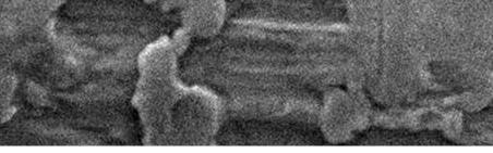
3 1.0 Background 1.1 Tin Whisker Phenomenon Unalloyed tin (Sn) plating has a long history of whisker formation and growth that has resulted in reliability problems for various types of electronic equipment. Tin Whiskers are essentially filaments or fibre like single crystals of tin which spontaneously grow from a tin surface during storage or use. This process can take anything from a few seconds to several years. As illustrated in Figure 1.1, there are several classified types of whisker. Filament whiskers are needle like in as much as the length is at least ten times the diameter. Column and spiral whiskers are quite self explanatory. Nodule whiskers are normally defined by their diameter and are often referred to as mounds or hillocks. (a) Filament whisker with striations (b) Column whisker with a consistent cross section (c) Spiral whisker (d) Spiral whisker growing from a nodule Figure 1.1 Examples of tin whisker appearance [1] The key reason why tin whiskers are problematic in the electronics industry is evidenced by the list of failures caused by whisker growth. The growth of tin whiskers has resulted in failures in many critical and non critical systems ranging from space and military applications through to failures in medical, industrial and computer applications. In essence it is safe to say that any electrical or electronic application which utilises tin or tin alloys has the potential for tin whisker growth which could, in turn lead to failure. 3

 to the tin plating.")
 plating, leaving essentially pure tin.")

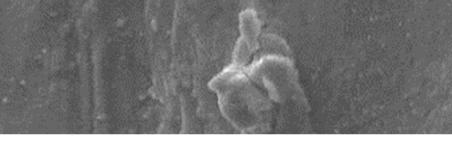
4 1.2 Tin Whisker Mitigation Despite many years of global study, there is presently no definitive explanation as to how or why tin whiskers form. One of the more prevalent theories is that they are the result of stress relief within tin plating, or perhaps form as a result of recrystallisation and abnormal grain growth within the tin grain structure. It is sufficient to say that until the mechanisms behind the growth of tin whiskers are properly understood prevention remains difficult. Historically the predominant whisker mitigation strategy has been the addition of lead (Pb) to the tin plating. However RoHS legislation that has eliminated the use of lead in most electronic products sold in the European Union has led electronic components manufacturers, including TT Electronics, to action the removal of lead from tin-lead (SnPb) plating, leaving essentially pure tin. This approach is the most convenient and least costly lead elimination strategy for the majority of component manufacturers. However, for the high-reliability user, the pure tin presents reliability risks due to the whisker forming tendencies of pure tin and tin alloy plating, which can electrically short across component terminals or break off the component and degrade the performance of electrical or mechanical parts, as shown in Figure 1.2. Tin Whisker Component Termination Figure 1.2 Example of a tin whisker growing from a component termination [1] There is however a great deal of new information in the public domain on tin whisker formation and strategies for migrating to lead free surface finishes. Moreover the number of accepted methods of mitigation to reduce the risks of whisker growth is constantly growing. Some of the more recognised whisker reduction methods include [2]: Adding a nickel (Ni) underlay between the tin plating and a copper (Cu) base metal mitigates whisker formation. The underlying plating may alleviate the compressive stress in the tin film, which is thought to be one of the driving forces for tin whisker growth. Adding a silver (Ag) underlay between tin plating and copper base metal has been proposed as a method to mitigate whisker formation, similar to Ni as above. Hot dip tin is a molten bath process often used for electronic component terminations, which is considered to be whisker free. Hot dipping with tin-silver-copper (SnAgCu) is generally an effective mitigation practice. 4


5 Matte tin is a tin film with lower internal stresses and larger grain sizes than so called bright tin and is therefore less prone to whisker formation. Matte and bright tin finishes are defined by the following: Parameter Matte Sn Bright Sn Carbon Content 0.005%-0.050% 0.2%-1.0% Grain Size 1µm-5µm 0.5µm-0.8µm When added to tin in amounts of 2-4% by weight, bismuth (Bi) may aid in suppressing whisker growth. With lead free solder, SnBi is a viable candidate for component finishes. With Eutectic tin lead solder, it is necessary to control the bismuth content of the finish between 3-5% so as to have enough bismuth to suppress whisker formation without getting into the compositional range of the ternary eutectic. In addition, keeping the bismuth content low is required to retain solderability of formed leads. In practice the most common lead free finishes adopted by industry are matte tin on nickel underlay, hot dipped tin and SnAgCu alloy 2.0 Testing 2.1 Test Sample Preparation TT Electronics manufactures an extensive range of resistive components. However there are effectively only three main termination materials used in the production of these parts as detailed in Figure Termination Finish Under Layer Base Metal Products Used On Matte Sn plating Ni plating Dipped Ag SMD resistors Hot dipped Sn None Cu wire Epoxy/cement coated resistors Hot dipped SnAgCu Ni plating Cu clad Vitreous enamel coated Steel wire resistors Figure Main termination materials used at TT Electronics Samples manufactured with each of the above terminations were taken as being representative of a production batch and were then soldered on to circuit boards ready for testing as shown in Figure (a) Matte Sn plating (b) Hot dip Sn (C) Hot dip SnAgCu Sample mounting for testing 5


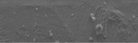
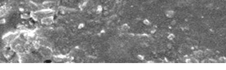
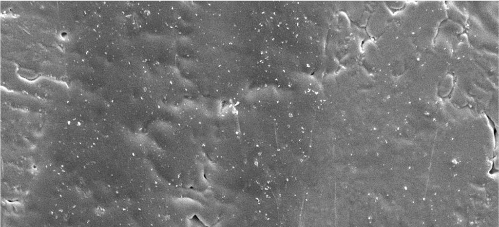
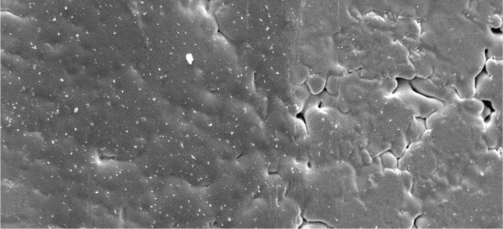
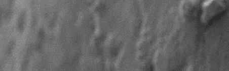
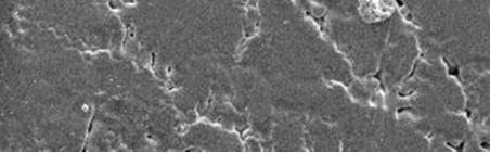
6 2.2 Testing and Inspection Method The following tests were conducted in accordance with JEDEC Standard; JEDEC JESD22-A121A [1] and JEDEC 201A [3], see Figure Test Type Test Conditions Interim Inspection Total Duration Temperature Cycling -40 to +85 o C, air to air; 30min soak; ~1 cycle/hr 75 cycles 6000 cycles Ambient Temperature/ 50 ± 2 o C and 60 ± 3% RH 4000 hours hours High Temperature/ 60 ± 2 o C and 93 ± 3% RH 4000 hours hours Figure Testing procedures Analysis of the terminations took place at the interim inspection interval and after completion of the tests. The areas of inspection on each of the three terminations types are depicted in Figure (a) Matte Sn plating (b) Hot dip Sn (C) Hot dip SnAgCu Figure Areas of inspection for the three termination types Inspection for tin whiskers was carried out using a scanning electron microscope (SEM). Firstly a screening inspection was conducted at a magnification of x250 followed by a detailed inspection at a magnification of x Results A summary of all results is presented in Figure 3.1 and detailed SEM images of examples from all tests are shown in Figures 3.2 (a) to (r). Test Description No. of Tin Whiskers of Length 5µm Found at Inspection Matte Sn plate Hot dip Sn Hot dip SnAgCu Interim Final Interim Final Interim Final Maximum Permissible Whisker Length Temperature Cycling µm Ambient Temperature/ µm High Temperature/ µm Figure 3.1 Summary of test results (Note: minimum whisker length detectable at x1000 magnification 5µm) 6


 Cycling 2")


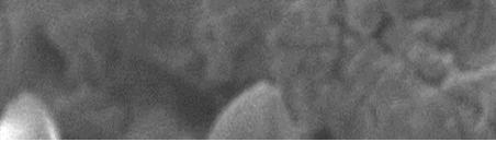
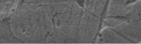
7 2 3.2 (a) Temperature Cycling Matte Sn Plating, x (b) Temperature Cycling Matte Sn Plating x (c) Temperature Cycling Hot dipped Sn, x (d) Temperature Cycling Hot dipped Sn, x (e) Temperature Cycling Hot dipped SnAgCu, x (f) Temperature Cycling Hot dipped SnAgCu, x1000 7


")
")

")
")

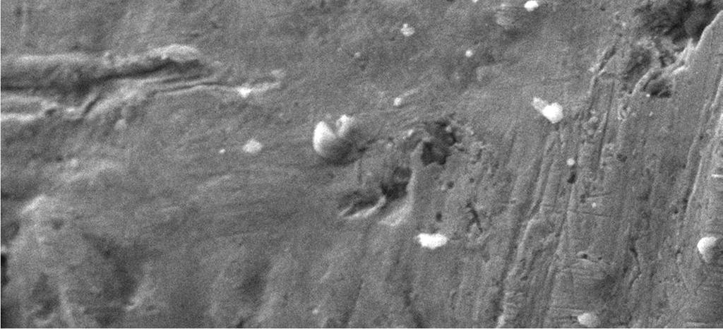
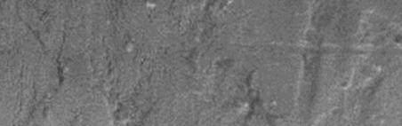
8 2 3.2 (g) Ambient T/H Storage Matte Sn Plating, x (h) Ambient T/H Storage Matte Sn Plating, x (i) Ambient T/H Storage Hot dipped Sn, x (j) Ambient T/H Storage Hot dipped Sn, x (k) Ambient T/H Storage Hot dipped SnAgCu, x (l) Ambient T/H Storage Hot dipped SnAgCu, x1000 8


")


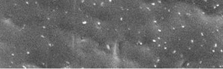
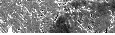
9 2 3.2 (m) High T/H Storage Matte Sn Plating, x (n) High T/H Storage Matte Sn Plating, x (o) High T/H Storage Hot dipped Sn, x (p) High T/H Storage Hot dipped Sn, x (q) High T/H Storage Hot dipped SnAgCu, x (r) High T/H Storage Hot dipped SnAgCu, x1000 9
10 4.0 Discussion As can be seen from the above results there was no evidence of tin whisker growth on any of the samples tested. This result is very encouraging and indicative of the success of the mitigation methods applied to TT Electronics resistor products. All three of the termination materials tested incorporates one or more of the mitigation methods discussed in Section 1.2; the two termination wire types are hot dipped, a technique which is considered to be whisker free. In addition a SnAgCu finish is applied to the steel core wire to further enhance this measure. The plating applied to the SMD components is matte tin with a nickel underlayer, of which both materials are considered to be good mitigation measures. The result is further supported by the extended test cycle durations undertaken. As can be seen from Figure 4.1 the actual total test durations are much greater than those recommended in JEDEC Standards. Test Type Total Test Duration JESD201A Actual Temperature Cycling 1500 cycles 6000 cycles Ambient Temperature/ 4000 hours hours High Temperature/ 4000 hours hours Figure 4.1 Comparison on JEDEC Recommended and TT Electronics Actual test durations 5.0 Conclusions No evidence of tin whiskers were found on any of the components tested. Mitigation methods used appear to be successful in preventing the growth of tin whiskers on all three termination materials used by TT Electronics. 6.0 Disclaimer The data and conclusions presented in this report are for information only and no guarantee of performance is intended to be expressed or implied. Users of TT Electronics resistors for critical applications are responsible for the extent to which they rely upon this information. 10
11 7.0 References 1. JEDEC JESD22-A121A Measuring Tin Whisker Growth on Tin and Tin Alloy Surface Finishes, July inemi Recommendations on Lead-Free Finishes for Components in High Reliability Products, Version 3, May JEDEC 201A Environmental Acceptance Requirements for Tin Whisker Susceptibility of Tin and Tin Alloy Surface Finishes, September Bibliography Galyon, George T (2004): A history of Tin Whiskers Theory: 1946 to 2004 New York NASA, NASA Goddard Space Flight Center Tin Whisker (and Other Metal Whisker) Homepage IEC, (March 2004) 91/443/NP: New Work Item Proposal: IEC : Environmental testing Part 2 82: Test Test Tx: Whisker test methods for electronic and electric components. IEC, (April 2005) 91/517/CD: Committee Draft: IEC : Environmental testing Part 2 82: Test Test Tx: Whisker test methods for electronic and electric components. 11