The Effects of Aging on the Reliability of Lead Free Fine-Pitch Electronics Packaging. Jiawei Zhang
|
|
|
- Lee Bradley
- 5 years ago
- Views:
Transcription
1 The Effects of Aging on the Reliability of Lead Free Fine-Pitch Electronics Packaging by Jiawei Zhang A dissertation submitted to the Graduate Faculty of Auburn University in partial fulfillment of the requirements for the Degree of Doctor of Philosophy Auburn, Alabama August 4, 2012 Keywords: aging, lead-free, creep, fine-pitch, electronics packaging, reliability Copyright 2012 by Jiawei Zhang Approved by John L. Evans, Thomas Walter Professor of Industrial and Systems Engineering Robert Neal Dean, Associate Professor of Electrical and Computer Engineering Richard Sesek, Assistant Professor of Industrial and Systems Engineering Michael J.Bozack, Professor of Physics
2 Abstract A direct and deleterious effect on packaging reliability has been observed during elevated temperature isothermal aging for fine-pitch ball grid array (BGA) packages with Sn-1.0Ag-0.5Cu (SAC105), Sn-3.0Ag-0.5Cu (SAC305), and Sn-37Pb solder ball interconnects. Package sizes ranging from 19 mm with 0.8 mm pitch BGAs to 5 mm with 0.4 mm pitch BGAs with three different board finishes (ImSn, ImAg and SnPb) were evaluated. The aging temperatures were 25 o C, 55 o C, 85 o C, and 125 o C, applied for a period of 6 months. Subsequently, the specimens were thermally cycled from -40 o C to 125 o C with 15 min dwell times at the high temperature. Weibull analysis of failures vs. cycle number show a ~ 50% reduction in package lifetimes when aged at 125 o C compared to room temperature, with less dramatic but measurable reductions in lifetime at 85 o C and even 55 o C. In contrast, the reliability performance of Sn-37Pb is much more stable over time and temperature. The degradation was observed for both SAC alloys on all tested package sizes and board finishes. For the 19 mm SAC105 case, for example, there was a 53% (32%) reduction of characteristic lifetime at 125 o C (85 o C) compared to room temperature aging. The trends were in the expected directions; namely, the reliability was reduced when using higher aging temperatures, smaller solder balls, and SAC105. The dominant failure mode can be associated with the growth of Cu 6 Sn 5 intermetallic compounds (IMC) during the aging, particularly on the pad side. In a second portion of this work, longer aging with more different type packages have been investigated. The degradation rate becomes slower compared with 6 months aging, but ii
3 continuous reduced lifetime cycles are observed. The microstructures of these packages have been examined and correlated to their mechanical properties and reliability performance. iii
4 Acknowledgments The author would like to thank his advisor Dr. John L. Evans for his support, guidance and mentorship throughout this research. Sincere gratitude and appreciation are also extended to my committee members, Dr. Robert Dean, Dr. Richard Sesek and Dr. Michael J. Bozack for their valuable insights and precious time in the course of this research. The author particularly thanks Dr. Michael Bozack for his corporation and many discussions regarding the progress of the lead-free soldering project. Thanks are also extended to all my lab-mates, coworkers and friends, Zhou Hai, Doctor Yifei Zhang, Sivasubramanian Thirugnanasambandam, and John Marcell, for their encouragement and friendship. The author is in debt to his parents, who support him endlessly although they are so far away. iv
5 Table of Contents Abstract... ii Acknowledgments... iv List of Tables... viii List of Figures... ix List of Abbreviations... xii Chapter 1 General Introduction Soldering Alloys in Electronics Performance Characteristics of Solders Component Finish-Lead Free Solder Candidate Pure Tin Sn-Zn Sn-Cu Sn-Bi Sn-Ag Sn-In Sn-Ag-Cu (SAC) Sn-Ag-Cu Solder Alloys Mechanical Properties of Solder Joint Tensile Properties...11 v
6 1.5.2 Shear Properties Creep Fatigue Lead-Free Printed Circuit Board Surface Finishes Issues in developing Lead-free SMT Assembly Process Background of Electronic Packaging Evolution Plastic Ball Grid Array Packages Outline of the Dissertation Chapter 2 Literature Review Introduction Effects of Aging Solder Joints Thermal Aging Effects Thermal Aging Microstructure Evolution Kirkendall Voiding and Effect on Reliability Impact of design and material choices Impact of Reflow Profile Impact of Design and Reliability Lifetime Prediction Models for Solder Joint Fatigue Stress-Strain Modeling Constitutive Modeling of Creep Deformation Anand Viscoplastic Model vi
7 2.5 Review: Lifetime Prediction Models for Solder Joint Fatigue Chapter 3 Experimental Approach Introduction Test Board Design-Test Vehicle (TV7) Electronic Package Selection Components Selection Solder Paste and Stencils SMT Assembly Processes Inspection Test Vehicle Issue about Double Sides ImSn Board Finish Experimental Testing Methods Test Matrix and Test Conditions Data Acquisition System Failure Analysis Chapter 4 TV7_1 Reliability and Failure Analysis TV7 Reliability Analysis Resistors mm PBGA mm PBGA mm PBGA vii
8 mm PBGA TV7 No Aging and 6 Month Aging Failure Analysis Discussion and Conclusion Chapter 5 TV7_2 Reliability and Failure Analysis TV7 Reliability Analysis mm PBGA mm PBGA mm PBGA mm PBGA Fine-Pitch CSP and QFN Aging Microstructure Failure Analysis Discussion and Conclusion References viii
9 List of Tables 1.1 Important Characteristics of Solders Alloys Comparison of Surface Finishes Typical Thermal Operating Environments Effects of Design Parameters on the Fatigue Life of BGA Nomenclature Used for the Anand Constitutive Model Summary of Solder Joint Fatigue Models TV7 Component Matrix Lead Free Solder Paste Parameters in TV Stencil Specifications for TV TV7 Thermal Accelerated Reliability Test TV7 Thermal Testing Plan ix
10 List of Figures 1.1 The Market Share of Different Lead-Free Solder Typical 3-D Ternary Phase Diagram Sn-Ag-Cu Ternary Diagram View of Sn-Ag-Cu Microstructure of SAC Alloy Summary of Failure Mechanisms in Microelectronic Packaging Typical Stress-Strain Curve of Lead-free Alloys Solder Joints Subjected to Shear Strain during Thermal Cycling WSBGA Creep Curve of Lead-free Solders Creep Deformation Map of Solder Alloys Lead-Free Assembly Process Impact Comparing Sn-Pb and SAC Process Window Evolution of Electronic Packaging Technology Basic Electronic Packaging Function BGAs Are Correctly Positioned during Reflow Soldering ITRS: Trend of BGA Technology Cross-section of PBGA ITRS: Trend of BGA Technology x
11 2.1 Room Temperature Aging Effects on Sn-Pb Solder Joints Deduction in Ball Shear Strength at RT SAC Creep Rate Comparison Ratio of Maximum Creep Rate SAC Reflowed Aging Voids Reflow Recommended for Lead-free Packages Flow chart for Fatigue Life Modeling Methodology Example of Product Usage Cycle TV7 Dimension TV7 Layout TV7 Test Vehicle for Lead Free TV7 Test Vehicle for Tin-Lead Continental electronics Prototype Manufacturing lab Reflow Oven Reflow Profile Process Flow of SMT Borads Assembly Test Board after Reflow X-ray Images Double sided ImSn Board Finish AES Spectra for the Borad Finish TCT Testing Profile xi
12 3.15 TST Testing Profile Weibull Plot-2512 Resistors Weibull Plot-19mm BGAs Isothermal Annealing conditions for 19mm SAC Isothermal Annealing conditions for 19mm SAC Weibull Plot-15mm BGAs Isothermal Annealing conditions for 15mm SAC Isothermal Annealing conditions for 15mm SAC Weibull Plot-10mm BGAs Weibull Plot-5mm BGAs Isothermal Annealing conditions for 5mm SAC Isothermal Annealing conditions for 5mm SAC Backscattered electron images SEM microstructure Package and board side IMC thinckess Failure mode for 19mm BGAs Failure mode for 0.4mm pitch BGAs Failure regions for 0.4mm pitch BGAs Weibull 19mm BGAs Isothermal Annealing conditions for 19mm SAC Isothermal Annealing conditions for 19mm SAC Weibull Plot-15mm BGAs xii
13 5.5 Isothermal Annealing conditions for 15mm SAC Isothermal Annealing conditions for 15mm SAC Weibull Plot-10mm BGAs Weibull Plot-5mm BGAs Isothermal Annealing conditions for 5mm SAC Isothermal Annealing conditions for 5mm SAC Weibull Plot-7mm CSPs Weibull Plot-5mm QFNs SEM microstructure of 19mm SAC SEM microstructure of 10mm SAC SEM microstructure of QFNs xiii
14 PBGA ENIG SMT JEDEC PCB RoHS SEM NSMD WEEE CTE Symbols Ag Cu Im Pb Sn List of Abbreviations Plastic Ball Grid Array Electroless Nickel Immersion Gold Surface Mount Technology Joint Electron Device Engineering Council Printed Circuit Board Restriction of Hazardous Substances Scanning Electron Microscopy Non solder mask defined Waste from Electrical and Electronic Equipment Coefficient of Thermal Expansion Silver Copper Immersion Lead Tin Greek Symbols β Slope η Characteristic Life ρ Probability plot Subscripts T g Glass Transition Temperature xiv
15 Chapter 1 General Introduction 1.1 Soldering Alloys in Electronics Soldering is a metallurgical joining process in which two or more metal items are joined together by melting a filler metal into the joint. The filler metal with melting point below 425 is called solder [1]. As metal joint, the use of solder alloys can be dated back to thousands of years. In the electronics material world, solder interconnects have three major roles: thermal, electrical, and mechanical. The quality of the solder is crucial to the integrity of a solder joint, which in turn leads the overall functioning of the assembly. From the history of the electronics industry, the solder used is primarily 63Sn-37Pb (a eutectic composition), or 60Sn-40Pb (a near eutectic composition). The Sn-Pb binary system has a relatively low melting eutectic temperature of 183 and is compatible with most substrate materials and devices. According to recent reports, Pb in Sn-Pb solder contributes many technical advantages, [2, 3]: - Pb improves the wetting ability by reducing the surface tension of pure tin. - Pb provides ductility to Sn-Pb solder alloys. 1
16 - Pb prevents the transformation of β-tin to α-tin, which will cause %26 volume increase and loss of structural integrity. - As a solvent metal, Pb helps tin and copper to form intermetallic bonds by diffusion. - Pb is inexpensive and readily available. Sn-Pb has relatively low melting temperature of 183, which allows low reflow temperature in electronics packaging process and prevents the high temperature negative effect on the boards and components. However, the harmful effect of lead to humans is well known. Amount of electronic waste ends up in landfills and the lead will leach into soil [4-13]. More and more concerns and pending legislation push forward lead free solders used in global electronics market. The European Commission s (EC) adopted two directives, Waste Electrical and Electronic Equipment (WEEE) and the Directive of Restriction of the Use of Certain Hazardous Substance (RoHs), both ban the use of lead from end-of-life electrical or electronic components after July1, 2006 in European Union countries. In Japan, there is no government ban of lead in electronics components, the advisory committee of Japan Institute of Electronics Industry Development Association (JEIDA) creates a roadmap for lead-free solders and gives recommendations for industry. In the United States, the U.S. environmental Protection Agency (EPA) and IPC (the Institute of Interconnecting and Packaging Electrical Circuits) have also proposed a roadmap for the lead-free movement in U.S.. Therefore, developing practical alternative Lead-free solders for electronics packaging is important. 2
17 1.2 Performance Characteristics of Solders The solder alloys used in microelectronics have strict performance requirements [14]. First, the solder alloy needs the qualified electrical and mechanical performance. Second, the solder must be suitable to all aspects of electronics manufacturing process, which include: the solder must have desired melting temperature. It must adequately wet common PCB pads, form inspectable solder joints, allow high volume soldering and rework of defective joints, and provides reliable solder joints during service conditions and low assembly cost. The properties of solders both for manufacturing and reliability are summarized in Table 1.1 [14]. There are some basic criteria for perfect lead-free alternatives [15, 16]: - Similar melting temperature to existing Sn-Pb solders in order to have similar reflow manufacturing profile. - Good wettability to ensure good metallization during manufacturing process. - Equal or better electrical properties to efficiently transmit the electrical signals. - Adequate mechanical properties to provide the reliability of the electronic packaging products. - Non-toxic and relatively low price. 3
18 Table 1.1 Important Characteristics of Solders Alloys Manufacturing Melting/liquidus temperature Wettabilitty (of copper) Cost Environmental friendliness Availability and number of suppliers Manufacturability using current processes Ability to be made into balls Copper pick-up rate Recyclability Reliability Electrical conductivity Thermal conductivity Coefficient of thermal expansion Shear properties Tensile properties Creep resistance Fatigue properties Corrosion and oxidation resistance Intermetallic compound formation Ability to be made into paste 1.3 Component Finish-Lead Free Solder Candidate There are a large number of Pb-free options, and these solder alloys include binary, ternary and some quaternary alloys. More than 70 alloys were identified in the literature [14]. Among these alloys, a large number are based on Sn as the primary or major constituent Pure Tin Sn becomes the principal components of most solder alloys because Sn can wet and spread on a wide range of substrates. Elemental Sn has melting temperature at 231 and exists in two forms with different crystal structures. β-tin has a 4
19 body-centered tetragonal crystal structure and is stable at room temperature. α-tin has a diamond cubic crystal structure and is thermodynamically stable below 13 [14]. The transformation from β-tin to α-tin happens when the temperature falls below 13, which is referred as tin pest or tin disease. It will lead to volume increase and cracking in the tin structure. For most of the devices, the cycle is cross the 13, therefore, when tin is exposed to thermal cycles, plastic deformation and cracking at gain boundary happens. Also Tin is prone to whisker growth, elements (Bi and Sb) can suppress whisker growth in tin [17-19] Sn-Zn SnZn was one choice to replace SnPb due to its cheaper and low melting temperature of around 198, and the processing temperature can be even lower by addition of bismuth-sn8zn3bi to 192. The eutectic structure consists of two phases: a body centered tetragonal Sn Matrix phase and a secondary phase of hexagonal [20]. Sn-Zn is reactive because both Sn and Zn interact with Cu to form intermetallic phases. However, SnZn solders are prone to form hard paste to oxidation and some issues including wetting problems Sn-Cu The Sn-Cu binary alloy solder has a eutectic composition of Sn-0.7 wt.% Cu with a eutectic temperature of 227. The low price of this alloy is attractive, but in the reflow process, it has poor properties and is prone to whisker growth Sn-Bi The eutectic Sn-Bi of 42Sn-58Bi is potential alternative for Sb-Pb with its low 5
20 melting temperature of 139 [21-23]. Wettability of 42Sn-58Bi is acceptable and its low temperature mechanical properties are better than Sb-Pb alloy. It is reported that cracking in the alloy may occur at slow cooling rate since Bi in Sn will precipitate in the Sn phase as the alloy cools. Large grains forms during slow cooling rate, and crack occurs between these large grain boundaries Sn-Ag The Sn-Ag (Sn-3.5 Ag) binary system has eutectic temperature of 221. The microstructure consists of Sn and Ag 3 Sn. Addition of 1% Zn is shown to improve the solidification microstructure by introducing finer and uniform dispersion of Ag 3 Sn. However, the poor performance on the wetting blocks its wide use in industry Sn-In The eutectic composition of In-49.1Sn has eutectic temperature is 117. Due to the low melting temperature, Sn-In has been used in SMT applications. However, Indium price is even more expensive than silver, and low availability. The Sn-In solder alloys are not popular in the electronics packaging industry. 1.4 Sn-Ag-Cu (SAC) The Sn-Ag-Cu (SAC) alloy has been the prevailing alloys system in major electronics manufacturing [24-27]. There alloys [28] include 96.5Sn-3.0Ag-0.5Cu (SAC 305) in Japan, 95.5Sn-3.9Ag-0.6Cu (SAC 396), and 95.5Sn-4.0Ag-0.5Cu (SAC 405) used for BGA solder joint, in addition, recently for portable electronics, more and more manufacturers are using SAC 105. The benefits of SAC over other Pb-free alloy systems include relatively low melting temperature, good mechanical and 6
![solderability properties. Soldertec surveys [29] show 70% of the lead-free alloys market is SAC series, Fig.1.1. There are still some changes for SAC series alloys.](/docs-images/86/93300395/images/21-0.jpg "First, SAC series alloys have higher melting temperature around 217, which need higher reflow profile in process and leads to reliability issues.")
21 solderability properties. Soldertec surveys [29] show 70% of the lead-free alloys market is SAC series, Fig.1.1. There are still some changes for SAC series alloys. First, SAC series alloys have higher melting temperature around 217, which need higher reflow profile in process and leads to reliability issues. Second, the excessive formation of intermetallic compounds at the interface between solder joints and copper pad can cause reliability problems. Thirds, SAC alloys cost more than Sn-Pb. Fig.1.1 The Market Share of Different Lead-free Solders [29] Sn-Ag-Cu Solder Alloys In the Sn-Ag-Cu eutectic or near eutectic series alloys, SAC alloys contain % of Ag and % of Cu. The eutectic melting temperature was 217 with 4.7 wt.% Ag and 1.7 wt.% Cu. Loomans and Fine [30] refined the composition as 3.5 wt.% Ag and 0.9 wt.% Cu. Figure 1.2 shows one 3-D ternary phase diagram. The lowest point or temperature in the isothermal lines is the eutectic composition. The eutectic reaction formulation is: 7
 Sn and Ag react to form and Sn and Cu react to form (Fig.")
22 The 2-D of the ternary phase diagram of Sn-Ag-Cu shows in Figure 1.3. The red region is near eutectic region. Most popular SAC alloys is in this region with around melting temperature of 217. Figure 1.2 Typical 3-D Ternary Phase Diagram ( Sn and Ag react to form and Sn and Cu react to form (Fig. 4-5), these intermetallic compounds have much higher strength than Sn-Pb, which block the fatigue movement of dislocation. SAC alloys have 3-4 times better fatigue properties than Sn-Pb eutectic solders [32]. 8

 Front View of Sn-3.8Ag-0.")
23 Figure 1.3 Sn-Ag-Cu Ternary Phase Diagram ( Figure 1.4 (a) Top view of Sn-3.9Ag-0.6Cu [31], (b) Front View of Sn-3.8Ag-0.7Cu Solder Bumps (T.Y. Lee at UCLA). 9

24 Sn+Cu 6 Sn 5 Sn+Ag 3 Sn Figure 1.5 Microstructure of SAC Alloy 1.5 Mechanical Properties of Solder Joint The solder joints of electronic device are subjected to mechanical stresses and strains during operation. The primary cause of the stresses and strains is due to different coefficient of thermal expansion between electronic component and the board and between die and packaging body. The failure of the solder connections can be classified into three parts: electrical, mechanical and corrosion failures. A summary of the failure mechanisms in electronics packaging is shown in Figure 1.6. Fatigue and fracture of solder joints lead to most failure of electronic devices. When operation temperature changes, the solder balls are subjected to shear strain, which is because of the difference of CTE. As the operation temperature cycles, the solder balls are subjected to cyclic shear strain. The CTE mismatch factors include: the range and frequency of the temperature, the design of the component and solder 10
25 joint distribution, the solder joint geometry, and the solder alloy elastic-plastic and creep constitutive relationships. When the boards or substrate are bent during manufacturing process or handling, the solder joints can also meet tensile loading. Tensile and creep properties are critically important for the reliability of the electronic device. Figure 1.6 Summary of Failure Mechanisms in Microelectronic Packaging Tensile Properties The tensile properties of lead free solder, such as Young s modulus, yield strength, ultimate tensile strength (UTS) are necessary to determine the solder joint reliability of electronic packages (BGA, CSP, QFN). Yielding is defined as the material will deform elastically and will return to its original shape when stress is removed. The applied stress that causes yielding is defined as the yield stress (YS). 11
26 The ultimate tensile stress (UTS) is the maximum load divided by the initial cross-sectional area of the specimen. Engineering stress and engineering strain are defined as followed [38]: (1.1) (1.2) Where P is applied stress, is initial cross-sectional area, is final gage length, is initial gage length. A typical stress-strain curve of lead-free is shown in Figure 1.7. Figure 1.7 Typical Stress-Strain Curve of Lead-free Alloys The elastic modulus is the slope of the elastic portion of the stress-strain curve. In engineering practice, 0.2 % of plastic deformation is used as Yield Stress. 12

27 1.5.2 Shear Properties Solder joints of electronic devices have shear loading most of the time, which is generated by the CTE mismatches. In thermal cycling condition, CTE mismatches lead to cyclic shear stresses on the solder connections. Figure 1.8 shows one example of flip chip packages, and the stresses are generated between the silicon and substrate [14]. Figure 1.9 shows WSBGA 54, assembled with SAC solder, failed at 1639 cycles in thermal cycling [100]. Similar to tension properties, shear properties include shear modulus and shear strength. The shear modulus G can be calculated if elastic modulus E and Poisson s ratio are given [38]: (1.3) Figure 1.8 Solder Joints subjected to Shear strain during Thermal Cycling due to CTE Mismatch 13
![Figure 1.9 WSBGA 54, Assembled with SAC Solder, Failed at 1639 Cycles in 0-100 Thermal Cycling [99] 1.5.3 Creep Electronic devices are also subjected to long periods of constant elevated temperatures.](/docs-images/86/93300395/images/28-0.jpg "Creep deformation causes the solder joints to fail under a constant load at elevated temperatures.")
28 Figure 1.9 WSBGA 54, Assembled with SAC Solder, Failed at 1639 Cycles in Thermal Cycling [99] Creep Electronic devices are also subjected to long periods of constant elevated temperatures. Creep deformation causes the solder joints to fail under a constant load at elevated temperatures. The homologous temperature is defined as the ratio of the temperature of the material and its melting temperature in degrees Kelvin [41]. (1.4) When is greater than 0.5, creep is considered as the dominant solder deformation mechanism in SMT [41]. For the typical thermal testing profile -40 to 125, of Sn-Pb is to 0.87, of SAC is 0.48 to 0.81, both are in the rapid creep deformation range. Creep is time-dependent strain plastic deformation. When solder material is exposed with a constant load at a long constant temperature, the creep of solder joints shows three stages: primary creep, secondary creep and tertiary creep. Figure
29 shows a typical lead-free creep curve, which include the three stages above [42]. In the first stage, the strain rate decreases rapidly over time due to strain hardening, which restricts the deformation. In the second stage, if is greater than 0.5, most of the plastic deformation creep will occur in this stage. In the third stage, necking and micro-cracking will occur. Eventually creep rupture will occur. There are many creep mechanisms that have been studied. Nabarro-Herring Creep is believed to be the dominate deformation mechanism with low stress at high temperature. If there is no pressure, atoms in the lattice will migrate in proportion to the gradient of the concentrations. The lattice defects tend to move in directions that will relieve the imbalance of pressure [44], then which will lead to creep deformation. Grain-boundary sliding is another creep deformation at high temperatures. It is associated with other deformation mechanisms. If is greater than 0.5, the stress mainly determines the creep deformation mechanism. For low level stress, the creep deformation will be lattice diffusion and grain-boundary diffusion. At intermediate stress, dislocation creep will dominate. At high stress level, dislocation gliding will be the main contribution for the creep. Figure 1.11 shows the creep deformation map of the solder alloys. 15
30 Figure 1.10 Creep Curve of Lead-free Solders Figure 1.11 Creep Deformation Map of Solder Alloys 16
31 1.5.4 Fatigue Fatigue occurs when a material is subjected to cyclic loading. Fatigue failure is caused by localized stress concentrations. Due to CTE mismatches between two adjacent materials, displacement leads to crack initiation and crack propagation. Cracks initiate at the sites of stress concentration such as micro-cracks, indents, dislocation slip steps, etc.. We should note that even when the cyclic stress is below yield stress, fatigue failure still can occur at defects and irregularities in the microstructure. Fatigue failure is sudden, catastrophic, and involves little plastic deformation. Ductile materials often behave as if they were brittle when subjected to fatigue. The fatigue damage is cumulative, and the materials can not recover when load is removed. There are three stages for a fatigue failure to fully develop and occur [99]: Stage 1: Crack nucleation Cracks initiate at the sites of stress concentration (micro-cracks, scratches, indents, interior corners, dislocation slip steps, etc). Stage 2: Crack propagation occurs in two steps: I: Initial slow propagation along crystal planes with high resolved shear stress. Fracture formed in this step features flat surface. II: Faster propagation perpendicular to the applied stress. Cracks grow by repetitive blunting and sharpening process at crack tip. Stage 3: Ultimate failure, where cracks eventually reach critical dimension and propagate very rapidly. 17
32 1.6 Lead-Free Printed Circuit Board Surface Finishes From July 1, 2006 RoHS compliance has established of new set of regulations restricting circuit board manufacturers to use of lead-free finishes. There are various protective finishes available. Considering cost and availability, there are some finishes popular in industry, which include: Organic Solderability Preservative (OSP), Hot Air Solder Leveling (HASL), Immersion Silver ImAg and Immersion Tin ImSn, Electroless-Nickel Immersion Gold (ENIG). - OSP s is designed to coat a thin, uniform protective layer on the copper surface of PCB s. OSP s finishes are inexpensive, and provide good surface oxidation, coplanarity and good process control. The drawbacks of OSP s include poor shelf life, degrades with high temperature, poor wettability and very poor electrical testability. - Lead-Free-HASL is the predominant surface in industry for a long time. The process consists of immersing circuit boards in a tin/lead alloy and the excess solder is removed by blowing hot air across the board. It is the lowest cost, but lead process is banned from 2007, leaf-free HASL experiences difficulty in controlling thickness and has thermal shock the boards during process. - ImAg offers good wettability, good shelf life, good coplanar and is suitable for multi-process reflow. The only problem for ImAg is slow uptake of technology. - ImSn is another alternative surface finish. Similar to the advantages of ImAg, ImSn is very poor for reflow cycles. 18

33 - The properties of ENIG are the best among these lead-free board finishes. Excellent wettability and coplanarity, excellent surface oxidation and electrical testability. The disadvantage of ENIG is higher cost and black pad which is referred as the nickel layer is prone to break up during mechanical stress. There is table 1.2 shown properties of different surface finishes. And NEMI Users Group has published a PCB finish rating in Table 1.3 [48]. Table 1.2 Comparison of Surface Finishes Finish Recommend Risky Not Acceptable No Vote Immersion Ag Immersion Sn OSP ENIG HASL (SnCu) Table 1.3 NEMI Users Group PCB Finish Rating 19
![1.7 Issues in developing Lead-free SMT Assembly Process Figure 1.12 shows the impact of using lead-free on the SMT assembly process [45].](/docs-images/86/93300395/images/34-0.jpg "Most popular lead-free alloys have a melting temperature of 35-40 higher than eutectic Sn-Pb, which is melting at 183.")
34 1.7 Issues in developing Lead-free SMT Assembly Process Figure 1.12 shows the impact of using lead-free on the SMT assembly process [45]. Most popular lead-free alloys have a melting temperature of higher than eutectic Sn-Pb, which is melting at 183. According to Kester report, the key process variables for Lead-free SMT assembly are listed below. - Melting temperature of solder alloy - Flux Chemistry activation, temperature effects - Wetting and surface tension properties of the alloy - Solder balling and bridging potential increase - Component/ board reliability - Compatible rework / repair Figure 1.12 Lead-Free Assembly Process Impact 20

35 The high reflow profile shrinks the process window dramatically in Figure Reflow profile significant impacts wetting and microstructure of the solder joint, which is critical to the performance of lead-free solder joints. Figure 1.13 Comparing Sn-Pb and SAC Process Window The flux in higher temperature issues include increased paste slump and charring of the slump. Solder paste manufacturers are using resins and gelling agents, which are stable at higher preheats and higher peak reflow temperatures, and offer good hot slump resistance and activators. 1.8 Background of Electronic Packaging Evolution Electronic Package is defined as an electronic structure that protects an electronic or electrical element and its environment from each other [35]. From the silicon to the printed wiring board level, technologies all belong to packaging hierarchy. One packaging evolution is shown in Figure Silicon efficiency is the percentage of the functional Printed Circuit Board (PCB) area taken by the silicon. 21
36 The function of an IC package is to protect, power, cool the microelectronic device and play a role as a bridge for electrical and mechanical connection as in Figure1.15. The trends of higher speed, small package size with higher I/O, and low cost requirements push peripheral array evolve into area array package like Pin Grid Array (PGA). Surface mount technology uses solder joints directly to attach the package on the board, which saves more surface area for additional components and reduce the electrical parasitic because of shorter interconnect length. Ball Grid Array (BGA) and Chip Scale Package (CSP) meet most of the requirement of today s microelectronics industry. CSP and BGAs are the most prevalent package types in portable hand held consumer electronics. CSP can even achieve the package size to silicon size ratio of 1.2. BGAs have become popular because they have robust balls at higher pitches instead of fragile leads like QFP. And BGAs are self-alignment during reflow even if they are misplaced by 50%, i.e. during reflow, an BGA that has not been properly placed, will float back to its optimal position on the solder lands thanks to surface tension forces, as shown in Figure They can obtain higher I/O count for a given substrate area, reduce component size, weight and cost, easier manufacturing process especially for placing machine, furthermore, they can extend to multichip modules like 3-D Packaging. Figure 1.17 shows recent trends of the BGA technology. Fine pitch, even micro pitch BGAs, can meet the demand of interconnect density increase with pitch size reduction. Quad Flat No Leads (QFN) is another surface mount technology, similar to CSP, 22


37 with a planar copper lead frame substrate. Compared with BGAs and CSPs, QFN has better thermal performance due to exposed copper die-pad technology. Figure 1.14 Evolution of Electronic Packaging Technology [36] Figure 1.15 Basic Electronic Packaging Function Figure 1.16 BGAs Are Correctly Positioned During Reflow Soldering 23
, shown in Figure 1.18, is made of high temperature PCB laminate.")
38 Figure 1.17 ITRS: Trend of BGA Technology Plastic Ball Grid Array Packages Plastic ball grid array (PBGA) is a low cost and low profile package. The plastic ball grid array (PBGA), shown in Figure 1.18, is made of high temperature PCB laminate. Bismaleimide triazene (BT) resin has a high glass transition temperature and is the most commonly used resin for PBGA. PBGAs have most of the BGAs advantages, however, there are some major issues with PBGA. First, PBGA packages are extremely moisture sensitive and larger PBGAs are susceptible to warpage. Second, it is difficult to rework for the underneath balls. The low coefficient of thermal expansion (CTE) of silicon die contributes greatly to the failure of the solder balls failure of PBGA. CTE mismatch between die and packaging body can cause solder joints to fail. Solder mask defined (SMD) and non-solder mask defined (NSMD) are two solder mask designs used with PBGAs. Each design has its own advantages and drawbacks. But the biggest issue for SMD is 24


39 the sharp edges formed in the solder balls where stress concentrations can occur. Examples of these two types of solder mask pads are in Figure Figure 1.18 Cross-section of PBGA [Courtesy: Amkor] Figure 1.19 Solder Mask Defined and Non Solder Mask Defined 1.9 Outline of the Dissertation The dissertation is divided into the following chapters: Chapter 1: Introduction to electronics packaging evolution and Pb-free soldering technology, alloys and board finish. Chapter 2: Present literature survey on lead-free assembly process, room 25
40 temperature aging effects, elevated thermal aging effects. Chapter 3: Description of the testing vehicle part I and manufacturing process and the experimental procedures. Chapter 4: Long term of aging effects on the thermal reliability of Pb-free BGAs, CSP and QFN and microstructure evolution analysis. Chapter 5: Description of the testing vehicle part II and manufacturing process and the experimental procedures. Chapter 6: Short term of aging effects on the thermal reliability of Pb-free BGAs, CSP and QFN and microstructure evolution analysis. Chapter 7: Summary and conclusions of the dissertation. 26
41 Chapter 2 Literature Review 2.1 Introduction Lead-free soldering of electronic packaging has attracted more research and development from both industry and academic institutes with the agreement on the implementation of the WEEE/ROHS legislation in Europe and market trends. Surface mount technology changed the function of solder joints from simply supplying the electrical connection to offer including the mechanical reliability. Most lead free alloys require higher reflow temperatures, which needs different assembly processes. Not only the package level reliability but also board level reliability is a primary concern. A lot of solder alloys have been examined, only a few can meet the baseline requirements of manufacturability, cost, availability and reliability. Even though thousands of technical papers have tried to discover the mechanical properties of lead-free, the actual impact of these lead free replacement alloy systems on the board level is not well understood, especially across the different package types [47]. There are a variety of main causes. First, due to different lead-free solder joints in real electronic packages, and package variables include die size, package size, ball count, pitch, mold compound and substrate material, it is difficult to obtain mechanical 27
42 properties from bulk solder. Second, due to complex material properties of solder joints in electronic packages, the impact of different environmental stresses on the microstructure and thermo-mechanical reliability has discrepancy. Accelerated testing is mostly used in finding the reliability of lead-free solders. Thermo-mechanical solder fatigue is the main failure mechanism in solder joints, which is the key failure for those applications whose service lifetime is expected to be a few years or longer. The most common accelerated reliability test is temperature cycling. And for the typical thermal testing profile [49], here is shown in table 2.1. Electronics Consumer Industry Automotive Military Operating Temperature 0 C to + 70 C -40 C to 85 C -40 C to +125 C -55 C to +125 C Table 2.1 Typical Thermal Operating Environments [49] There are few previous studies on the impact of isothermal aging on board level solder joints. However, most solder alloys have a high homologous temperature even in room temperature. Unlike eutectic tin-lead, the microstructure and mechanical behavior of Sn-Ag-Cu serial alloys degrades over time at room temperature and especially more rapidly during elevated temperature. When electronic devices are subjected to long periods of constant elevated temperatures, the microstructure and mechanical behavior of solder alloys can change significantly over time during long term isothermal aging. Most manufacturing components are stored at room 28
43 temperature for a prolonged period of time before assembly, and during manufacturing assembly, the solder alloys are exposed to elevated temperature, which results in aging of the second level solder joints [52]. Even though some researchers have begun to study the isothermal aging on solder joints, more accelerated tests and field data are necessary before getting conclusions about the long-term reliability of lead-free solder material and the trend of effects of thermal aging on different package designs. It is useful to set up reliable constitutive models for solder alloys in order to assess solder joint stress/ strain analysis and predict solder joint life. Solder joints show complicated creep-plasticity interaction and temperature-strain rate dependent material characteristics during operation. Current finite element models do not evolve with material aging. There will be significant error in calculations with the new free SAC alloys. It is indeed necessary investigate constitutive modeling of solder alloys. 2.2 Effects of Aging on Solder Joints The microstructure, mechanical, response, and failure behavior of lead-free solder joints in electronic assemblies are constantly evolving when exposed to isothermal aging and/ or thermal cycling environment [46, 47, 51-59]. And most common reliability threat comes from stress-relaxation, which is based on thermal fatigue damage. And the most common accelerated reliability test is elevated temperature isothermal aging and/ or thermal cycling. And the material behavior [51] during test includes reduction in stiffness, yield stress, ultimate strength, strain to failure and accelerated creep. And even room temperature aging can affect the 29
44 behavior of lead-free solder joints [51, 59, 60, 61]. For tin-lead solder joints, in 1976, Lampe reported that when Sn-Pb and Sn-Pb-Sb solder alloys stored for 30 days at room temperature, losses in shear strength and hardness were up to 20%, as shown in Figure 2.1. and Medvedev [61] found 30 % loss of tensile strength of bulk Sn-Pb solder compared to 23% loss for solder joints for 435 days. The aging effect on a specific operating condition and solder joint is different. Lee et al. also observed that during 3 days room temperature aging after reflow the shearing stress of solder joints decreased by up to 10 % [62,63], which is shown in Figure 2.2. Figure 2.1 Room Temperature Aging Effects on Sn-Pb Solder Joints 30

45 Figure 2.2 Deduction in ball shear strength at RT Xiao studied the stress-strain curve of SAC396 during different durations of room temperature aging, and there are losses of ultimate tensile strength up to 25 % at room temperature over days [64, 65]. Xiao elevated SAC396 temperature aging at 180. At this highly elevated temperature, they observed a quick softening of the material during the first 24 hours followed by a gradual hardening with time Thermal Aging Effects There are widely published studies about thermal aging effects at elevated temperatures, they found dramatic changes in the microstructure and mechanical properties. Darveaux [67] performed an extensive experimental study on the stress-strain and creep behavior of area array solder balls subjected to shear. He found that aging for 1 day at 125 caused significant effects on the observed stress-strain and creep behavior. The aged specimens were also found to creep much faster than un-aged ones by a factor of up to 20 times for both SAC305 and SAC405 solder alloys. Some studies [58, 69 71] have been performed on the degradation of BGA ball 31
46 shear strength with elevated temperature aging at 125 or 150. And all these studies documented microstructure coarsening and intermetallic layer growth during the aging period. Chiu found significant reductions in drop reliability during elevated temperature aging [58], voids formation and coalesce is to be the dominant mechanism for solder joint strength and board level reliability degradation. And Ding, et al. [68] explored the evolution of fracture behavior of SnPb tensile samples with elevated temperature, cracks propagated across the Sn-dendrites and Sn-Ag eutectic structure. Some papers have studied under aging effects the relationship between solder joint and substrate finish. Lee et al. in Cisco [72] investigated the interaction between isothermal aging and the long-term reliability of fine-pitch ball grid array (BGA) packages with Sn-3.0Ag-0.5Cu-0.5Cu solder interconnects. Two different surface finishes with 0.4-mm fine-pitch packages with 300-μm-diameter Sn-Ag-Cu solder balls were used. During thermal cycles from 0 to 100 with 10 min dwell time, they found package lifetime was reduced by around 44% by aging at 150. Aging at 100 showed smaller impact but similar trend. In Auburn, CAVE Research has studied aging effects on solder for more than 10 years. The microstructure, mechanical response, and failure behavior of lead free solder in electronic assemblies are constantly evolving when exposed to isothermal aging and/or thermal cycling environments. Ma, et al. [51, 66] demonstrated that the observed material behavior variations of SAC305 and SAC 405 lead free solders during isothermal aging at 125 were unexpectedly large and universally 32
47 detrimental to reliability. The measured stress-strain data demonstrated large reductions in stiffness, yield stress, ultimate strength, and strain to failure (up to 50%) during the first 6 months after the reflow process. After approximately 1000 hours of aging, the lead free solder joint material properties were observed to degrade at a slow but constant rate. Even more dramatic evolution was observed in the creep response of aged solders, where up to 500X increases in the secondary creep rates were observed for aging up to 6 months. And the degradation of lead SAC solder joints is much larger than the corresponding changes occurring in traditional 63Sn-37Pb assemblies. Most important observation from Ma, et al. research is the cross- over point. For 125 aging of lead-free and lead, this cross-over point occurred after around 50 hours of aging, and marked the point where lead free solders began to creep at higher rates than 63Sn-37Pb. But such phenomenon was not observed for solder joints aging at room temperature. Zhang.et al [103] demonstrated the significant effects of elevated temperature exposure on the creep behavior of solder joints. And the creep rates evolved more dramatically when temperature was increased. In addition, the effects of aging were shown to be significant even for aging temperature slightly above room temperature (e.g. T = 75 o C). In addition, the lower silver content alloys (e.g. SAC105) were observed to be much more sensitive to aging (have greater changes in the creep rate for a given aging time) than the higher silver content alloys (e.g. SAC405). Ma.et al [104] investigated aging effects in solders for aging durations of up to 6 months. Thermal aging significantly decreases the mechanical properties of both SAC 33
48 and Sn-Pb solder alloys. Compared to the room temperature aging described in the previous study, the aging at elevated temperatures has a much more significant effect on the mechanical properties (stress-strain and creep). The aging effects are more significant at higher aging temperatures and for longer aging durations. There is a cross-over point at about 200 hours of aging at elevated temperatures where the creep resistances of the SAC alloy becomes lower than that of Sn-Pb. Zhang.et al [105] continued to exam the effects of aging on mechanical behavior of lead free solders by performing stress- strain and the effects of aging on mechanical behavior of lead free solders have been examined by performing stress-strain and creep tests on four different SAC alloys (SAC105, SAC205, SAC305, SAC405) that were aged for various durations (0-6 months) at room temperature (25 o C), and several elevated temperatures (50, 75, 100, and 125 o C). Analogous tests were performed with 63Sn-37Pb eutectic solder samples for comparison purposes. Variations of the mechanical and creep properties were observed and modeled as a function of aging time and aging temperature. In addition, the chosen selection of SAC alloys has allowed us to explore the effects of silver content on aging behavior (we have examined SACN05 with N= 1%, 2%, 3%, and 4% silver; with all alloys containing 0.5% copper).the results obtained in this work have demonstrated the significant effects of elevated temperature exposure on the stress-strain and creep behavior of solder joints. As expected, the mechanical properties and creep rates evolved (degraded) more dramatically when the aging temperature was increased. In addition, the effects of aging were shown to be significant even for aging temperature 34
49 slightly above room temperature (e.g. T = 50 o C). The recorded data demonstrate that the material property (stiffness and strength) degradation becomes linear with aging time. The creep rate evolves (increases) in an exponential manner, and the behaviors of lead free and tin-lead solders experience a cross-over point where the lead free solders begin to creep at higher rates than standard 63Sn-37Pb solder for the same stress level. In addition, the creep behaviors of the lower silver content alloys (e.g. SAC105) were observed to be much more sensitive to aging (have greater changes in the creep rate for a given aging time) than the higher silver content alloys (e.g. SAC405). The times required before the cross-over occurred were reduced when considering higher aging temperatures or SAC alloys with lower silver content. It was also observed that lowering of the silver content of a SAC alloy leads to increases in the creep rates for all aging conditions. However, the addition of dopants was also shown to lessen the aging effects. The degradations of the mechanical and creep properties of lead free SAC solders during aging are caused by microstructural evolution. In particular, there is dramatic coarsening of the secondary intermetallic particles. When the particles are small and fine precipitations, they can effectively block the movement of dislocations and reduce grain boundaries sliding, thus strengthening the materials and enhancing creep resistance. When the second phase particles grow larger, their ability to block the dislocation movements and grain boundary sliding are significantly reduced leading to reduced strength and to degraded resistance to creep deformations. Zhang, et al [50] extended to include a full test matrix of aging temperature and 35
50 solder alloys. The different alloys from SAC105 to SAC405 were aged for various durations (0-12 months) at 25, 50, 75, 100, and 125. And the results in this work have demonstrated the significant effects of the elevated temperature exposure on the creep behavior of solder joints, the effects of aging were shown to be significant even for aging temperature slightly above room temperature (e.g. T=75 ), as shown 2.3. In addition, the lower silver content alloys (e.g. SAC105) were much more sensitive to aging than high silver content alloys (e.g. SAC 405). And the times required before the cross-over occurred were reduced when considering higher aging temperature or SAC alloys with lower silver content. Table 2.2 shows ratio of creep rate to non-aged creep for 4 months at temperature 125. Figure 2.3 SAC Creep Rate comparisons (Aging at 75 ) SAC Alloy Maximum Aging Induced Increase in Creep Rate 36
51 SAC105 SAC205 SAC305 SAC X 1000X 220X 220X Figure 2.4 Ratio of Maximum Creep Rate to Non-Aged Creep Rate for Each SAC Alloy The relationship between solder ball reliability and substrate pad finish under aging conditions has also been studied. Hasegawa, et al. [101] observed the relationship of thermal aging at 150 for prolonged time on the reliability of Sn-Pb and SAC alloys on substrates with different PBGA surface finishes. Little change was observed in the mechanical strength (shear strength and elastic modulus). Zhou, et al. [102] studied the SAC 387 solder joint on both Cu and Ag substrate at an aging temperature of 170, and there was little effect on the SAC/Ag interface, but dramatically softened the SAC/Cu joint, which was due to lower residual stresses at the SAC/Ag joint interface Thermal Aging Microstructure Evolution Thermal Aging effects reduce the mechanical strength of solder alloys. And some studies [51, 67, 69, 73] shows it is related to a micro-structure coarsening process. When the gain structure is coarser, there are fewer gain boundaries to block the dislocation movement, causing strength loss of material. The continuous degradation of the mechanical properties is caused by the dramatic coarsening of the secondary intermetallic particles. When the particles are small and fine precipitations, 37
52 they can effectively block the movement of dislocations and reduce grain boundaries sliding, thus strengthening the materials. When the second phase particle grows coarser, their ability to block the dislocation movements and grain boundary sliding, which are known to be the major reason for creep failure, are significantly reduced. the SAC solder coarsening is shown in Figure 2.5. Fan [74] investigated Aging effects on the microstructures of 63Sn-37Pb, Sn-3.5Ag and SAC405 solder balls on Cu/Ni/Au surface finish. The thickness of the IMC layers all increased with aging time and temperature. 63Sn-37Pb has the larger diffusion coefficient and the IMC thickness grow rapidly. Li et al [75, 76] studied microstructure of flip-chip packaging with SAC387 solder joints aging at different temperature. The facet-like morphology of interfacial IMC (Cu,Ni)6Sn5 remained unchanged during aging, but its thickness increased considerably by a volume diffusion mechanism. The Sn IMCs existed as plate-like or lamella-like phases or as small particles around the β-sn dendrites in the bulk solder. Two different temperature aging: first, small Sn coarsening processes took place under high Sn particles directly coarsened into pebble-like phases and second the plate and lamella Ag3Sn phases broke up into small parts and then coarsened into pebble-like phases. 38

 The vacancies coalesce into voids with time and higher temperature. Chiu et al.")
![[58] reported tests of ball grid arrays (BGAs) with Sn-Ag-cu solder balls with Cu pad thermal aging at 100, 125, 150, and 175 for 3, 10, 20, 40 and 80 days.](/docs-images/86/93300395/images/53-3.jpg "They found extensive Kirkendall voids at the interface of solder joint to Cu substrate. The voiding process is activated even at 100. And after 10 days aging at 125.")
53 (a) (b) (c) Figure 2.5 (a) SAC Reflowed, No aging (b) 50 hours at 125 (c) 100 hours at Kirkendall Voiding and Effect on Reliability The formation of Kirkendall voids at the solder/cu interface has been reported for many years. The interdiffusion of Cu and Sn leads to void in solder joints. There are two steps for this process. (1) Cu atoms leave the Cu pad and diffusion towards the solder, which generated vacancies near the Sn layer. (2) The vacancies coalesce into voids with time and higher temperature. Chiu et al. [58] reported tests of ball grid arrays (BGAs) with Sn-Ag-cu solder balls with Cu pad thermal aging at 100, 125, 150, and 175 for 3, 10, 20, 40 and 80 days. They found extensive Kirkendall voids at the interface of solder joint to Cu substrate. The voiding process is activated even at 100. And after 10 days aging at 125. The drop performance degraded 80%. Higher temperature will generate more voids during the same aging time, as shown in Figure

54 Figure 2.6 (a) 3 days aging at 125 (b) 40 days aging at 125 Date et al. [78] studied miniature Charpy tests on solder balls of eutectic Sn-Pb and near eutectic Sn-Ag-Cu bounded to Cu, and aged at 150 for up to 1000 h. After 500 h aging at 150 a lot of voids were observed in the Sn phase at the interface between solders and Cu. And with aging time increased, transition from ductile to brittle associated with the fracture inside the solder to within the interfacial intermetallic compound (IMC) phase was reported. Ahat el al [79] did a study of interface microstructure and shear strength of 96.5Sn-3.5Ad and 63Sn-36Pb-2Ag on Cu after aging at 150 for 0, 50, 250, 500 and 1000 h. The voids formed in the Sn phase with the aging time increased. The shear strength of both Sn-Ag and Sn-Pb-Ag decreased with the aging time. They also studied the fracture mode change from the mixture of solder and IMC at zero aging time, to complete fracture within IMC layer after 1000 h aging. Mei et al. [77] studies conditions for voids formation and voids effects on the electronic reliability. And from 9 cases studies, voids were found in high, low even 40
55 zero densities in samples of different cases after aging either for 20 days at 125 or for 5 days at 145. Voids were seen in thermal cycled assemblies. It seemed that the Cu plating process and the small concentration of Ni in either the solder or the substrate influences the void density and distribution. 2.3 Impact of design and material choices SAC305 was once dominated for Pb-free assembly. SAC305 is starting to lose favor with increased need for shock resistance in consumer products. Some manufacturers are switching to SAC105. SAC105 melts at about 227 about 10 higher than melting temperature of SAC305 at 217 and also performs poorly in thermal cycle testing. In the lead-free manufacturing process, the most challenged issue is requiring peak temperature to reflow the solder, which did more hostile environment to the components on the boards. Moisture of BGAs can further aggravate component reliability with lead-free reflow soldering. Internal delamination, cracks, bond lifting, die lifting and even pop-corning effects can occur. Kester have recommended the profile in figure 2.7 [80]. 41

56 Figure 2.7 Reflow Recommended for Lead-free Packages Impact of reflow profile The basic requirement of the reflow solder must wet and bound to metallic substrates, which means that substrates implies that a constituent of the solder must form intermetallic compounds with copper, nickel and other metals plating on the boards. The second requirement is that the solder must have a melting point low enough to be reflowed as a paste and high enough to stand up to operating temperature. As Li [81] reported, the reflow temperature, reflow time and number of reflows 42
57 affect the thickness of intermetallic layers. And the shear strength of Sn-3.8Ag-0.7Cu solders shows no changes for two reflows even up to 10 reflows, but is degraded by high temperature storage, neither has effects on Sn-35Pb solder joints. Pandher [82] showed the optimization of the reflow process for SAC solder alloys in order to achieve best joint reliability in BGA applications. The paper was summarized as: (1) lower peak temperature results in lower IMC failures which is one would have expected from the earlier IMC thickness results. (2) lower time above liquidus is generally positive in reducing interfacial fractures. (3) lower peak temperature with longer time above liquidus results in the lowest number of IMC failures. (4) higher temperature and longer time above liquidus leads to larger solder spread. Harrison et al. [83] reported that the eutectic Sn-Ag3.8-Cu0.7 alloy is the best all-round solution for lead-free reflow soldering. Reflow can be achieved at a relatively low temperature, reliability is at least comparable with conventional tin-lead solders. The increased melting point means the paste must protect the powder from oxidation to about 220. Overall low residue paste and paste with lower solids contents were found to be less robust with lead-free alloys and they need inert atmosphere reflow for optimum results. High solids pastes were found to give good result in lead-free reflow, as they survived better with higher preheat and reflowed temperatures Impact of Design and Reliability Darveaux et al. [84,85,87] characterized the impact of design and material choice 43
58 on solder joint fatigue life for fine pitch BGAs, which include die size, package size, ball count, pitch, mold compound and substrate material, test board thickness, pad configuration and pad size, he also compared different testing profile effects on the reliability. From these studies, they got these conclusions: - The row of joints near the die edge failed first under most of the test conditions. - Fatigue life increased by up to 6X as die size was reduced, - For a given die size, fatigue life was up to 2X longer for larger packages with more solder balls. - Mold compounds with higher filler content reduced fatigue life by up to 2X due to a higher stiffness and lower thermal expansion coefficient. - Once optimized, tape based packages have equal board level reliability to laminate based packages. - Solder joint fatigue life was 20% longer for 0.9 mm thick test boards compared to 1.6 mm thick boards due to a lower assembly stiffness. - For CSP applications, NSMD test board pads give up 3.1X life improvement over SMD pads. - Ramp rate and range of test temperature also effect the reliability, faster ramps and larger range will result in higher stresses and more creep in the solder. Ng et al. [88] investigated the design analysis of BGA packages, and concluded eleven key parameters to affect the life of BGA joints. Table 2.5 gives the list from that study. Suhling et al. [86] addressed the under-the-hood reliability of smaller PBGA packages 44
59 (15 and 17 mm), and increased BT substrate thickness and NSMD pad can enhance the reliability. And underfill can make smaller components to meet the typical automotive thermal cycling requirements. Table 2.2 Effects of Design Parameters on the Fatigue Life of BGA Ghaffarian [89] studied accelerated thermal cycling test methods used in current industry to characterize the interconnect reliability of BGA and CSP assemblies. A failure shift from solder joint to package may occur more often for miniaturized CSP packages. Near-thermal shock conditions induced the most damage on CBGAs. Increasing the maximum cycling temperature had a more damaging effect than a decrease in the minimum temperature. Fatigue rather than creep, is considered to be main damage mechanism below one-half of the absolute melting temperature. 45
60 Stam [90] found that depending on board and component metallisations and use environment, the reliability of the lead-free solders could perform better or worse than traditional lead based solders. Syed [87] reported that he compared the acceleration factor for eutectic Sn/Pb and Sn/4.0Ag/0.5Cu alloys from 0/100 to -40/125 thermal cycle conditions. While this acceleration factor is about 2 for Sn/Pb alloy, Sn/Ag/Cu alloy resulted in about a 315X reduction in life when tested -40/125 cycle. A similar acceleration factor was also found for other compositions of Sn/Ag/Cu alloy evaluated here. It is a very important result as this indicates that Sn/ Ag/ Cu alloy does not need to be better than Sn/Pb if both testing -40/125 or higher temperature. 2.4 Lifetime Prediction Models for Solder Joint Fatigue The integrity of solder joints is a major reliability concern in modern microelectronic packages. Thermal mismatch induced stresses can result in extensive plastic deformation at solder joints, which is responsible for the low cycle thermal fatigue failure of solder materials. A general expression for the strain was defined by Yang, et al. [106]: = (2.1) Or more explicitly by: = (2.2) where σ is the stress; is the strain; E is the modulus of elasticity; m is the reciprocal of the strain-hardening exponent; is the reciprocal of the strength coefficient; is the steady-state creep-rate which is a function of the applied stress; is the 46
61 amplitude of primary creep strain; and B and are material (deformation mechanism) constants for the creep response. The four terms on right-hand-side of equation (2.6) are the elastic, plastic, time-dependent primary creep and steady-state creep strain components respectively. This relation is also commonly known as the classical elastic-plastic-creep constitutive equation. It serves as the basis for constitutive modeling of the material behavior of solder alloys, and supports both stress-strain curve modeling and constitutive modeling of creep deformation Stress-Strain Curve Modeling Mechanical properties of solder alloys are necessary for the applications of finite element analysis to electronics packaging. Stress-strain curves are an extremely important graphical measure of a material s mechanical properties. Tensile testing data are used to develop constitutive models to describe the stress-strain responses and corresponding mechanical properties. Pang, et al. [191] developed a modified Ramberg-Osgood model to describe the temperature and strain rate dependent stress-strain curves for SAC387. The Ramberg-Osgood model for elastic-plastic behavior can be expressed as: (2.3) The modified temperature and strain rate dependent Ramberg-Osgood Model is described as: )= (2.4) The hardening exponent n and stress coefficient σ0 are temperature and strain rate dependent: 47
62 (2.5) (2.6) where In these relations, a and c are temperature coefficients; c and d are strain rate coefficients; and are reference temperature and strain rate respectively; is the melting temperature of SAC387 (217 C); and and are the hardening exponent and stress coefficient at the reference temperature and strain rate Constitutive Modeling of Creep Deformation Constitutive modeling of creep deformation is very useful to predict the end of life of electronic packaging using finite element analysis tools. Many models have been proposed and studied. The Dorn power law model and Garofalo hyperbolic sine model are the two most popular models among them [ ]. It is well known that the two models are given by: (2.7) =C (2.8) Where is the secondary creep strain rate; is the applied stress; a is a temperature independent parameter; R is the universal gas constant; T is temperature in Kelvin; A and C are material dependent constants; n is the stress exponent; and Q is the activation energy. The problem is these models are solely based on steady-state creep, but not including aging effects Anand Viscoplastic Model An accurate numerical modeling of the stress and strain fields in electronic 48
63 packages is significant for improving mechanical designs of electronic packages. The most commonly accepted models employing the finite element method for thermal fatigue life prediction analysis can be classified as: nonlinear slice model, global model with linear super elements and nonlinear solder, linear global model with a nonlinear submodel, nonlinear global model with a nonlinear submodel, nonlinear global model [110]. The components of an electronic package may exhibit temperature and time dependent material behavior. Their material behavior at the length scales characteristic of an electronic package is also usually different from that of bulk properties. Electronic solder alloys are utilized at high homologous temperatures due to their low melting points. Creep deformations are significant under such conditions. The solder behavior is dependent on strain rate, stress, and temperature due to its high homologous temperature. Unlike the time-independent plasticity law, the viscoplastic constitutive law does not rely on an explicit yield surface and the loading and unloading criterion. Instead, it utilizes an internal state variable, representing the resistance of the material to inelastic deformations. Creep deformation is time and temperature dependent, and the time-independent plastic deformation results in plastic strains depending on the yield surface and loading and unloading criterion. Among the various time-dependent constitutive laws for solder joints in electronic packages, the viscoplastic constitutive law by Anand is frequently used. And the Anand viscoplastic constitutive model embedded within the ANSYS finite element software has become a common tool for engineers studying electronic 49
64 packaging reliability. Anand s model consists of two coupled differential equations that relate the inelastic strain rate to the rate of deformation resistance. The strain rate equation is ) (2.9) and the rate of deformation resistance equation is } Where B=1- and (2.11) The definitions of these parameters are given in table
65 Table 2.3 Nomenclature Used for the Anand Constitutive Model 2.5 Review: Lifetime Prediction Models for Solder Joint Fatigue Solder joint fatigue is considered as low-cycle failure. Therefore almost all lifetime prediction models originate from the Coffin-Manson s equation (2.12) Where N is the number of cycles to failure, is the plastic strain range per cycles, n is an empirical material constant, and C is a proportionality factor. A fatigue failure always begins at a local discontinuity such as the area of stress concentration near the 51
66 solder/pad interface. Plastic strain accumulates each cycle resulting in failure. The acceleration factor (AF) can be defined based on equation (2.13) as follows AF= (2.13) Where and are fatigue life under two different cyclic loading conditions, which correspond to the plastic strain range and respectively. Equation (2.13) has been widely used since the field life can be related to a test life with an empirical material constant n if the plastic strain range at each loading condition can be calculated. There are two major steps in solder joint reliability modeling. First, a suitable solder constitutive equation has to be implemented into the finite-element model. The stress- strain results from the finite-element model is extracted by averaging the inelastic strain energy density as a failure parameter. Second, a solder fatigue model is needed to calculate the number of cycles to fatigue failure using the failure parameter extracted from the finite-element model results [ ]. In [113], the fourteen solder joint fatigue models were categorized into one of the five classes: stress-based, plastic strain-based, creep strain-based, energy-based and damage-based. Table 2.4 gives summary of solder joint fatigue models. 52
67 Table 2.4 summary of solder joint fatigue models As listed in Table 2.4 Coffin-Manson, Solomon, Engelmaier, and Miner have proposed solder joint fatigue models based on plastic strain. By applying Miner s linear superposition principal, plastic and creep strain can be accounted for in a 53
68 strain-based fatigue model. The model is shown in Eq.(2.14). (2.14) Where is the number of cycles to failure due to plastic fatigue and is obtained from Solomon s fatigue model. refers to the number of cycles to failure due to creep fatigue model shown in Eq.(2.15). (2.15) The number of cycles to failure is related to a constant C, which is dependent on failure criteria and solder microstructure. is the strain range due to matrix creep. This fatigue model is similar to a full method by Lau et al. as Strain Range Partitioning (SRP). In SRP, a typical hysteresis loop can be separated into four components: the plastic strain in tension and compression (PP), the creep strain in tension and compression (CC), the creep strain intension-plastic strain in compression (CP) and the plastic strain in tension-creep strain in compression (PC). is the fraction of the total inelastic strain range of the hysteresis loop. (2.16) Ng, et al [114] mentioned the modeling methodology for thermal cycling fatigue life prediction, which has been applied successfully for life predictions and design enhancement of various advanced IC packages shown in Figure 2.8. The first step to determine the failure criteria like the first-failure life, mean life or characteristic life from Weibull plot of the thermal cycling test data. The second step is to select the solder creep models. Then the strain energy density (SED) accumulated per cycle can be calculated from the finite element model. There are a 54
69 few modeling assumptions to compute the fatigue life. Darveaux presented the computation of fatigue life with using the crack initiation life or the crack propagation life as the dominant life prediction model. The respective life correlation constants can be computed by correlating the modeling and testing data using the least square method. 55
70 Figure 2.8 Flow-chart for Fatigue Life Modeling Methodology 56
71 Chapter 3 Experimental Approach 3.1 Introduction The fine pitch BGAs and CSP technology become popular not only in short term portable consumer electronic devices also serve long-term electronic products (greater than 5 years). At the same time electronics products trend become smaller size and maximum functions, weight saving and cost reduction. Dr. Vasudevan [92] reported last year that miniaturization with increased interconnect density is the consumer electronics trend. And BGA pitch/ feature size decreases with increase in board interconnect density with time (approximate 30-50% in six years), and in the near future 2014, pitch of BGA for harsh environment will meet less than 0.8 mm, high performance will get 0.5 mm, and hand held will reach 0.4 mm or less requirement. At the same time, the electronics industry is migrating to lead-free electronics, both to comply with government legislations and to increase market share through product differentiation. The manufacturing of lead-free electronic products involves assembling lead-free components to lead-free printed circuit boards using lead-free solder alloys. Key issues that are being addressed by academic and industry include 57
72 lead-free solder alloy selection, characterization of lead-free solder alloy properties and behavior under various stress loading conditions, lead-free manufacturing, logistics and intellectual property issues, and lead-free assembly reliability assessment [91]. The fine pitch and not mature lead-free technology posed several challenges from a reliability standpoint. Previous literatures [50 81] show that the microstructure and mechanical behavior of Sn-Ag-Cu soldering alloys can change a lot over time when exposed to isothermal aging. Electronics assemblies built with SAC solder joints are exposed to elevated ambient temperature for periods of time. Ma [51] studies that SAC alloys degradation under aging effect at different temperature. Unlike eutectic Sn-Pb, microstructure and mechanical properties of SAC alloys changes over time even at room temperature. At elevated temperature the changes occur more rapidly. So it is very important to understand the impact of aging on different electronics package design. Form the report [92], a product from the manufacturing factory to consumers, needs long cycle, which needs months or even years. So the aging effect on the hand held consumer products are also important. The effort focuses on utilizing current knowledge and resources to achieve the long-term reliability for electronics products. The approach is as follows: - In this study, we explored the effects of elevated temperature isothermal aging on the mechanical behavior of board level packages. A full test matrix of aging temperature and solder alloys was studied. The different alloys from SAC105 to SAC305 were aged for various durations (0, 6, 12 months) at 25, 55, 85, 58

73 and 125. We built a mixture of BGAs (SAC 105 and SAC 305) and CSP fine pitch packages, QFN, and 2512 resistor packages on two different board finishes. The test was also performed with 63Sn-37Pb eutectic solder samples for comparison purposes. - Three thermal profiles were used to analysis the different acceleration factors of the reliability. - This study also showed the trend of aging on different package designs. This study is helpful for academic and industry to guideline the research on the aging effect on the leaf free fine pitch package and reliability. Figure 3.1 Example of Product Usage Cycle [92] 3.2 Test Board Design- Test Vehicle (TV7) The design of the test vehicle, TV7 was an FR-406 glass epoxy laminated with a glass transition temperature ( ) of 170. The dimension of the board design is 59
74 X mm with a thickness of mm (measured laminate to laminate), shown in Figure 3.2. There are four circuit layers with reasonable copper distribution to provide copper balance and typical CTE for thermal cycle testing. The board was double sided and with board finishes as ImAg, ImSn as TV 7 part I, and will do other two board finishes as TV 7 part II. The unpopulated layout of the TV 7 is shown Figure 3.3. Figure 3.4 and Figure 3.5 show populated test vehicles for lead free, and tin-lead. Figure 3.2 TV 7 dimension 60

75 Figure 3.3 TV7 Layout 61
76 Resistors 19mm PBGA SAC305 10mm PBGA SAC305 15mm PBGA SAC105 QFN 10mm PBGA SAC105 19mm PBGA SAC305 19mm PBGA SAC105 5mm PBGA CSP 5mm PBGA SAC105 SAC305 Figure 3.4 TV7 Test Vehicle for Lead Free Resistors 15mm PBGA SnPb QFN 10mm PBGA SnPb 19mm PBGA SnPb 19mm PBGA SbPb 5mm PBGA CSP SnPb Figure 3.5 TV7 Test Vehicle for Tin-Lead 62
77 3.3 Electronic Package Selection Components Selection Daisy chain components provided by Practical Components will be used to allow for continuous sampling of component reliability through the accelerated life tests. TV7 was populated with both active and passive devices. The active components include different sized SnPb and Pb-free PBGA packages and QFNs. The QFNs measured is 5X5 mm and had a termination alloy of Sn. The fine pitch PBGA packages measured 5X5mm, 10X10mm, 15mmX15mm and 19mmX19mm. and had Sn-1Ag-0.5Cu (SAC105), Sn-3Ag-0.5Cu(SAC305), and 63Sn-37Pb three solder joints for each size fine pitch PBGAs. CSP packages were also studied, which was 7X7mm with 2 layer and the solder ball was SAC305. Lall, et al. [93] studied the BGAs and CSP reliability for harsh environment, and found that solder mask (SMD) pads fail much faster than the non solder mask pads (NSMD) pads in the thermal fatigue. All the TV7 project PBGAs components were using NSMD pads for better analysis of the aging effect on the reliability. The packages matrix is shown in Table 3.1. The resistors (passive devices) measured 6.3X3.2 mm and had a termination alloy of Sn. The industry standard naming convention of resistor sizes describes the length and with of its body in hundredths of an inch. The resistors used in this research will be referred to as 2512 resistors (i.e. the resistor measured 0.25 X0.12 ). Suhling [94] reported that chip resistors had been fabricated with 90Sn-10Pb solder terminations to match the Sn-Pb solder paste better and to avoid fillet lifting. Pure Sn 63
78 terminations had occurred as a part of the overall lead free initiative. The 2512 resistors had large body size and highest rated power dissipation and poor solder joint reliability. The 2512 resistors were mounted in banks that consisted of five resistors placed in series. The 2512 resistors were incorporated for control purposes to ensure that that the reliability data matched previous testing at CAVE. Package Body Die Size Ball/Lead Pitch Ball Alloys Type Size (mm) Count (mm) Alignment (mm) CABGA 19X X Perimeter SnPb, SAC105,SAC305 CTBGA 15X X Perimeter SnPb, SAC105,SAC305 CVBGA 10X10 5.0X Perimeter SnPb, SAC105,SAC305 CVBGA 5X5 3.2X Full Array SnPb, SAC105,SAC305 CTBGA 7X7 5.9X Perimeter SnPb, SAC305 MLF 5X5 4.5X Sn Table 3.1 TV7 Component Matrix Solder Paste and Stencils ImSn and ImAg were the two different surface finishes incorporated into this test 64
79 vehicle. For the tin-lead test vehicle, the components were assembled onto the PCB with no-clean-type 3-Kester 256 paste (Sn37Pb). The lead-free solder paste was used SAC 305 solder paste, which represented one of the most common assembly practices in industry today [95]. For the lead-free test vehicle, the components were built onto the PCB with no clean Senju305 M31-GRN360-k1MK-V, as shown in Table 3.2. Item ECO M31-GRN360-K1MK-V Test method Specification Alloy Composition Ag:3.5, Cu:0.75, Sn: J-STD-006 Balance Powder Shape Powder Grain Size Spherical Type 3 (25~45 μ m) J-STD , STM-12, J-STD Table 3.2 Lead Free Solder Paste Parameters in TV7 The stencil specifications for TV7 are shown in Table 3.3, the E-FAB Electroform stencil thickness mm ( in). The solder paste print machine used was MPM UP2000 HiE. 3.4 SMT Assembly Processes All the test vehicles TV7 were fabricated in Continental AG Huntsville Electronics Division. PBGAs were high moisture sensitivity, and popcorn effect is caused by moisture rapidly expanding during reflow and can result in package crack. Twelve hours before assembly, the PBGA packages were bake out in an oven at 150 to remove moisture and prevent a popcorn effect during the reflow process. 65
80 The lead-free solder paste used in this TV7 build was no-clean-type Senju305. And the SnPb solder paste was no-clean-type Kester 256. We ordered the E-FAB Electroform stencil with thickness mm ( in). The solder paste print machine used was MPM UP2000 HiE. The stencil and the PCB were positioned in the screen printer, the solder paste was pressed through the stencil with a rubber squeegee. The board was transferred out, and is inspected to ensure the alignment of the solder paste was properly centered on PCB pad sites. Make sure there was no bridging and void for the 0.4 mm pitch sites. Next the PCBs were placed into two placement machines. One was Assembleon MG-1, another one was Universal GSM-1. MG-1 used a tape and real feeder to place small components: Resistor, 5mmBGA, MLF, CSP and 10mmBGA. GSM-1 used a tray feeder to pick and place 15mm BGA and 19mm BGA components. Once the board was fed into the machine, the programmed algorithm began and all the electronic components were picked and placed onto the test vehicle in order. The board was check again in case of skewed package placement. Figure 3.6 shows the continental electronics prototype manufacturing lab. MATERIAL EFAB TREATMENT EFAB TYPE EFAB STENCIL THICKNESS METAL MASK SIZE (W x H) 24 INCHES X 24 INCHES STEP SINGLE FRAME BORDER POLY PRINTER TYPE MPM AP-25/27 FIDUCIALS HALF ETCH AND FILL 66


81 Table 3.3 Stencil Specifications for TV7 Figure 3.6 Continental Electronics Prototype Manufacturing Lab Figure 3.7 Reflow Oven A 13-zone Rehm V7 convection reflow oven was used for reflow shown in Figure 3.7. The reflow gas was nitrogen. The conveyor speed was 33.5 inch/min. the temperature was monitored for PBGAs 19mm, PBGAs 10mm and Resistor SAC alloys melting temperature was around 217, the reflow profile needed all the 67

82 lead-free component above that temperature. The peak temperature for PBGAs, and 252 for resistors. The time duration for PBGAs in the oven above the melting point 217 was around 52 to 55 seconds, and 61 seconds for resistors. In the Sn-37Pb assemblies thermal profile, the peak temperature of PBGAs was between 224 to 229. In this process, resistors had a peak temperature of 231. The time duration for PBGAs in the oven above the melting point 183 was around 60 to 65 seconds, and 67 seconds for resistors. By comparing two processes, there was a difference of 21 in the peak temperature by PBGAs. The Pb-free-reflow and Pb-reflow profiles used for the assembly are shown in Figure 3.8. Figure 3.9 shows the process flow for the SMT board assembly. Figure 3.10 shows test board after reflow. (a) 68
lead-free Reflow Profile and (b)lead Reflow Stencil Print Component Component Reflow Paste placement placement")
83 (b) Figure 3.8 (a)lead-free Reflow Profile and (b)lead Reflow Stencil Print Component Component Reflow Paste placement placement (resistors) (PBGAs, MLF) Check Check X-ray and Optical Inspection Figure 3.9 Process Flow of SMT Boards Assembly 69

 and skewed,")
84 Figure 3.10 Test Board after Reflow 3.5 Inspection Test Vehicle A X-ray tomography system was used inspect the quality of the solder joints in the assemblies. Figure 3.11 shows the x-ray image of good PBGA solder joints from assembled boards. The solder joint defects were also captured, the solder joint defects were grouped into three major types: shorts (bridging) and skewed, insufficient, which is show in Figure 3.12.Warpage of the PCB during higher temperature was hypothesized to be the problem. And all the boards were baked before assemblies, the same problem did not exhibit again. (a) 70
 71")
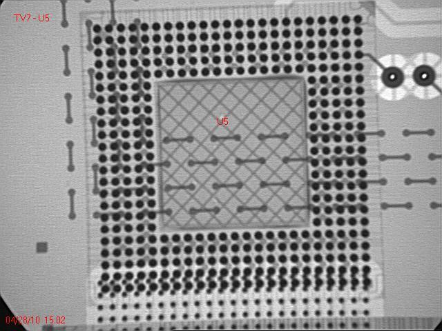
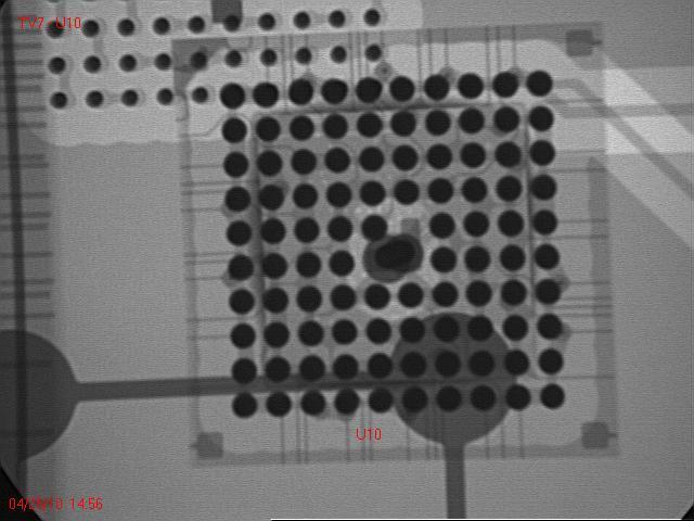
85 (b) (c) (d) 71

86 (e) (f) 72
 X-ray Image of 19mm SAC PBGA, (b) X-ray")
 X-ray Image of 5 mm SAC PBGA,")
 X-ray Image of 10mm Pb")
87 (g) (h) Figure 3.11 (a) X-ray Image of 19mm SAC PBGA, (b) X-ray Image of 15 mm SAC PBGA, (c) X-ray Image of 10 mm SAC PBGA, (d) X-ray Image of 5 mm SAC PBGA, (e) X-ray Image of 19mm Pb PBGA, (f) X-ray Image of 15mm Pb PBGA, (g) X-ray Image of 10mm Pb PBGA, (h) X-ray Image of 5mm Pb PBGA (a) 73
 is one of the most popular Pb-Free Surface Finishes, and Dr.")
![Schueller reported [96] that Immersion Tin composition is 17% of the surface finishes worldwide. But from [48] table, the solderability of double sided ImSn PCBs was a concern problem.](/docs-images/86/93300395/images/88-1.jpg "In the TV 7 Test Vehicle, we tried to built the double sided ImSn PCBs. The first side (Bottom) was good solderability, but the second side (top) exhibited very poor solderability.")
88 (b) Figure 3.12 (a) Skewed Pad Problem, (b) Shorts and Insufficient Problem 3.6 Issue about Double Sided ImSn Board Finish Immersion Tin (ImSn) is one of the most popular Pb-Free Surface Finishes, and Dr. Schueller reported [96] that Immersion Tin composition is 17% of the surface finishes worldwide. But from [48] table, the solderability of double sided ImSn PCBs was a concern problem. In the TV 7 Test Vehicle, we tried to built the double sided ImSn PCBs. The first side (Bottom) was good solderability, but the second side (top) exhibited very poor solderability. In the literature [96], insufficient thickness was reported as the failure reason. IMC growth through the thickness decreases solderability during storage or after second reflow. We used Auger electron spectroscopy (AES) to analyze the poor solderability for multi-reflow. AES is a true surface technique, allowing detection of all elements of the period table (except H) located within the first 50 Å of the material surface to a sensitivity of ~ 0.01 atom %. We reflow two ImSn boards for one time and two time 74
89 reflow. One observation of note was that the surfaces after LF profiles show a significant signal of Cu, probably due to increased interdiffusion between Sn and Cu to form an intermetallic compound during the higher temperatures employed with LF reflow profiles. Figure 3.13 shows the result of one time reflow and two time reflow AES spectra for ImSn. (a) (b) (c) (d) Figure 3.13 (a), (b) AES Spectra for The Board Finish Undergoing A LF, 1X Reflow, Before and After Sputter Cleaning. (c), (d) AES Spectra for The Board Finish Undergoing A LF, 2X Reflow, Before and After Sputter Cleaning. There were two main issues and solutions for this problem [96]. First, Exposure to humid conditions (>75%RH) can greatly accelerate oxide growth through the 75
90 creation of tin hydroxides. One recommended way was to use sealed moisture/ air tight wrapping for shipping and cool, low humidity storage. Second, contaminates break down the self-limiting nature of tin oxides and accelerate oxide growth. 3.7 Experimental Testing Methods Reliability of the solder joint of a particular package is defined as the probability that the solder joint will perform its intended function for a specified period of time, under a given operating condition, without failure. Numerically, reliability is the percent of survivors, R(t)=1-F(t), where R(t) is the reliability function and F(t) is the cumulative distribution function (CDF) [97]. Experimental evaluation of a solder joint reliability is often through accelerated reliability tests [98]. The most common accelerated reliability test is thermal cycling and thermal shock cycling. Because it simulates thermo-mechanical solder fatigue, which is the main failure mechanism in solder joints. The solder joints experience thermal-mechanical stresses combined with fatigue and creep. The ramp rates generate the CTE mismatch between solder joints and the surrounding materials, like the package die and PCB. Thermal shock is performed to exhibit sudden changed in temperature, within a short period time, cyclic exposed to an extremely high and low temperature. The steep ramp rate gives more mechanical stress on the solder joints Test Matrix and Test Conditions All the TV7 part I boards are testing follow three industry standard. For the Thermal cycling reliability test: thermal cycling (TCT) from -40 to 125 per JEDEC JESD22-A104B-Condition G, thermal cycling from -40 to 85 per 76
91 JEDEC JESD22-A104B-Condition G-condition A. For the thermal shock test thermal shock (TST) from -40 to 125 per JEDEC JESD22-A106-Condition A. The testing profile is shown in Table 3.4. Thermocouple results from one of the test boards are illustrated, as shown in Figure And Figure 3.15 shows the typical thermal shock profile. Test Type Low High Ramp Time Dwell Time Temperature Temperature (mins) (mins) ( ) ( ) TCT TCT TST Table 3.4 TV 7 Thermal Accelerated Reliability Test (a) (b) Figure 3.14 TCT Testing Profile (a) -40 to 125,(b) -40 to
92 Figure 3.15 TST Testing Profile Other aging boards were placed vertically in storage chamber at 25, 55, 85, and 125. The full matrix testing plan is shown in Table

93 Table 3.5 TV7 Thermal Testing Plan Data Acquisition System The Boards were placed vertically in the chamber and the wiring passed through the access port to the developed CAVE MarkDano data acquisition system. Monitoring of the various daisy chain networks was throughout the cycling using a high accuracy digital multimeter coupled with a high perpormance switching system controlled by LabView software. Based on IPC-9701, the practical definition of 79
94 solder joint failure is the interruption of electrical continuity > 1000 ohms. In this study, we defined the resistance became 300 ohms or above for continuous 5 times as resistance failure Failure Analysis Cross sectioning was used to establish failure within the solder by thermal fatigue cracking. Scanning electron microscopy (SEM) was used to investigate the microstructure of the joints. 80
95 Chapter 4 TV7_1 Reliability and Failure Analysis This chapter presents the interaction between 6 month isothermal aging and the long-term reliability of fine-pitch electronic packages located on the TV7 test vehicle. Microstructure analysis was conducted on different specimens. SEM was employed in order to obtain high quality micro-images of solder joints. The following sections will discuss the reliability data for the electronic packages and elevated isothermal aging effect on reliability of electronic packages. 4.1 TV7 Reliability Analysis The TV7 test vehicles were air to air thermally cycled between -40 to 125 with a 90 minute cycles time. Other thermal profile chambers had working problem issues, therefore the data will be published later Resistors The 2512 resistor banks consisted of five resistors placed in series. When one resistor failed, the other four resistors became censored data points. Figure 4.1(a)-(c) shows Weibull plots for the thermal cycling results on isothermally aged ImAg, ImSn 81


96 and SnPb 2512 resistor samples. A measurable degradation in reliability is observed for both resistors on ImAg and ImSn at elevated aging temperatures. Contrastingly, the SnPb parts were minimally affected by aging over the temperature. But after aging at 85 for 6 months, the SnPb parts were found ~%10 degradation. (a) (b) 82
97 (c) Figure 4.3 TV7 Weibull Plot 2512 Resistors on (a) ImAg (b) ImSn (c) SnPb Board Finish mm PBGA Fig. 5 shows Weibull plots for the thermal cycling results on isothermally aged SnPb, ImAg and ImSn 19mm BGA samples. A dramatic degradation in reliability is observed for both SAC alloys on ImAg and ImSn at elevated aging temperatures. Contrastingly, the SnPb parts were minimally affected by aging over the temperatures tested. In Fig. 5b, the characteristic lifetime for as-reflowed SAC105 on ImAg was 2559 cycles, while the characteristic lifetime was reduced to 1214 cycles after aging at 125 o C for 6 months. This is a 53% reduction in the characteristic lifetime. For 85 o C aging, there is a 32% reduction of lifetime. Fig. 5c shows the case for aged 83
98 SAC305 on ImAg. After 125 o C aging for 6 months, there was a 32% reduction of characteristic lifetime, compared 53% with SAC105 on ImAg. For the same package size (19mm) and aging conditions (125 o C/6 months), the characteristic lifetime of SAC alloys was much larger than Sn-37Pb solder. There is little change in reliability as a function of board finish. For SAC 105 on both ImAg and ImSn, the reduction in characteristic lifetime is 32% and 27% respectively; for SAC 305, it is 30% and 26% respectively. The Weibull plots show several clear trends: 1) higher Ag content improves the reliability of SAC alloys; 2) aging has a larger negative impact on reliability for fine pitch packages; 3) aging has little impact on the characteristic lifetime for SnPb; 4) higher aging temperatures result in higher rates of degradation for the SAC alloy solders tested; 5) only small changes in reliability were observed vs. board finish. (a) 84
99 (b) (c) 85
100 (d) (e) Figure 4.4 Weibull plots vs. thermal cycle for isothermally aged 19mm BGA samples (a) SnPb on SnPb (b) SAC105 on ImAg (c) SAC305 on ImAg (d) SAC105 on ImSn and (e) SAC305 on ImSn. 86
101 19mm BGA 3000 As-assembled 25C/6 month 55C/6 month C/6 month 125C/6 month Thermal cycling number SnPb ImAg-SAC105 ImSn-SAC105 Different board finish Figure 4.5 Weibull characteristic lifetime vs. isothermal annealing conditions for 19mm SAC105 BGAs on ImAg, and ImSn, compared to Sn-37Pb. 19mm BGA As-assembled 25C/6 month 55C/6 month 85C/6 month 125C/6 month Thermal cycling number SnPb ImAg-SAC305 ImSn-SAC305 Different board finish Figure 4.6 Weibull characteristic lifetime vs. isothermal annealing conditions for 19mm SAC305 BGAs on ImAg, and ImSn, compared to Sn-37Pb. 87
102 Figs. 4.6 and 4.7 show the characteristic lifetime for 19mm SAC105 (SAC305) on ImAg and ImSn compared to control Sn-37Pb. As assembled SAC alloy solders outperform Sn-37Pb but show dramatic decreases in lifetime with higher isothermal annealing temperatures. After 6 months of aging at 85 o C, the characteristic lifetimes of SAC on both ImAg and ImSn are lower than Sn-63Pb. While as assembled Sn-37Pb has a slightly worse characteristic lifetime than SAC alloys, it is much more stable over time and temperature mm PBGA The Weibull plots in Fig. 4.7 show the thermal cycling results on isothermally aged SnPb, ImAg and ImSn 15mm BGA samples. For the Sn-37Pb case (Fig. 4.7a), after 6 months of aging at 55 o C and 85 o C, the characteristic lifetime at both temperatures is reduced by only ~ 10% compared with no aging specimens. In contrast, the SAC alloys have similar or greater lifetimes than the as-assembled Sn-37Pb alloy, but degrade considerably during aging. For example, Fig. 4.7b shows that SAC105 on ImSn has a characteristic lifetime of 1429 cycles after 6 months of aging at 125 o C, which is ~ 50% lower than the lifetime (2926) of a no aging specimen. SAC305 performs better than SAC105 (Fig. 4.7c). In Fig. 8c, the cycle lifetime of SAC305 is ~ 45% lower than the lifetime (3742) of a no aging specimen. The results on ImSn have similar trends (Fig. 4.7d,e). Figs compare the characteristic lifetime vs. annealing precondition for 15mm SAC105 and SAC305 on ImAg and ImSn. All SAC solder alloys showed reduced characteristic cycle lifetimes with elevated annealing temperatures. 88

103 (a) (b) 89

104 (c) (d) 90
105 (e) Figure 4.7. Weibull plots vs. thermal cycle for isothermally aged 15mm BGA samples (a) SnPb on SnPb (b) SAC105 on ImAg (c) SAC305 on ImAg (d) SAC105 on ImSn and (e) SAC305 on ImSn. 91
106 15mm BGA Thermal cycling number 4000 As-assembled 25C/6 month 55C/6 month 85C/6 month 125C/6 month SnPb ImAg-SAC105 ImSn-SAC105 Different board finish Figure 4.8. Weibull characteristic lifetime vs. isothermal annealing conditions for 15mm SAC105 BGAs on ImAg, and ImSn, compared to Sn-37Pb. 15mm BGA Thermal cycling number 4000 As-assembled 25C/6 month 55C/6 month 85C/6 month 125C/6 month SnPb ImAg-SAC305 ImSn-SAC305 Different board finish Figure 4.9 Weibull characteristic lifetime vs. isothermal annealing conditions for 15mm SAC305 BGAs on ImAg, and ImSn, compared to Sn-37Pb mm PBGA 92
107 Weibull distributions for 0.4 pitch 10mm BGAs with SAC105 and SAC305 on ImAg are shown in Fig The relatively small volume of the solder balls was more sensitive to elevated temperatures at 55 o C and 85 o C than the cases reported above having larger solder balls. After 6 months of aging at 55 o C (85 o C), the cycle lifetime of SAC105 undergoes a ~ 27% (~ 38%) reduced lifetime compared with no aging specimens. (a) 93
108 (b) Figure Weibull plots vs. thermal cycle for isothermally aged 10mm BGA samples on ImAg (a) SAC105 (b) SAC mm PBGA The Weibull plots in Fig summarize the characteristic cycle lifetimes for isothermally aged 5mm BGA samples. Elevated anneal temperatures of 55 o C and 85 o C caused measurable losses in the characteristic lifetime of both SAC105 and SAC305. The characteristic lifetime for 5mm SAC105 BGAs on ImAg dropped from 4841 cycles as-assembled to 3087 cycles after aging at 55 o C for 6 months (36% reduction). The thermal reliability test results (Figs ) show that both SAC105 and SAC305 have better thermal resistance than Sn-37Pb at the as-assembled stage. After elevated temperature aging, however, the thermal performance degrades significantly. Increasing the Ag content in SAC alloys offers 94

109 some resistance for aging. For Sn-37Pb, the effect of elevated isothermal aging is insignificant. (a) (b) 95

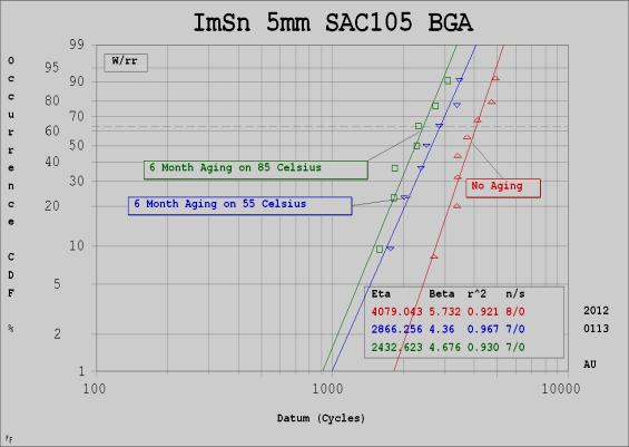
110 (c) (d) 96
 SnPb on SnPb (b) SAC105 on ImAg (c)")
111 (e) Figure Weibull plots vs. thermal cycle for isothermally aged 5mm BGA samples (a) SnPb on SnPb (b) SAC105 on ImAg (c) SAC305 on ImAg (d) SAC105 on ImSn (e) SAC305 on ImSn. 97
112 5mm BGA As-assembled 25C/6 month 55C/6 month 85C/6 month 125C/6 month Thermal cycling number Figure SnPb ImAg-SAC105 ImSn-SAC105 Different board finish Weibull characteristic lifetime vs. isothermal annealing condition for 5mm SAC105 BGAs on ImAg and ImSn, compared to Sn-37Pb. 5mm BGA As-assembled 25C/6 month 55C/6 month 85C/6 month 125C/6 month Thermal cycling number SnPb ImAg-SAC305 ImSn-SAC305 Different board finish Figure Weibull characteristic lifetime vs. isothermal annealing condition for 5mm SAC305 BGAs on ImAg and ImSn, compared to Sn-37Pb. 98
113 4.2 TV7 No Aging and 6 Month Aging Failure Analysis Failure mechanics of the thermally cycled PBGA packages is that the solder joint failure of PBGAs was attributed to the interaction between fatigue and creep. Shear stresses affect on solder joint creating tension and compression forces during the heating and cooling cycle. The CTE mismatches between the silicon die, PBGA substrate and printed circuit board generated these shear stresses. The degradation in Weibull characteristic cycle lifetime is related to the microstructure evolution of solder joints. Figure 4.14 shows backscattered electron images of the SAC105, SAC305 and Sn-37Pb alloy microstructures before and after aging at 125 o C/6 months. The characteristic starting microstructure of SAC alloys contains a -Sn matrix with imbedded Ag 3 Sn second phase particles. SAC alloys with greater Ag content have higher Ag 3 Sn particle densities. After aging at elevated temperatures, it is clear that the Ag 3 Sn particles undergo coarsening caused by solid state diffusion [103]. Specifically, the coarsening of alloy grain and phase structure is governed by the self-diffusivity of atoms, interstitials, and vacancies, given by an Arrhenius relationship [116] (4.1) where D is diffusivity, is a constant, k is the Boltzmann constant, Q is the activation energy, and T is the absolute temperature. Since coarsening is highly dependent on temperature, it is likely that the diminished reliability of SAC alloys under elevated temperature annealing is in part connected to the increased ability of 99

 Ag 3 Sn Ag 3 Sn 10 m")
 SAC105;")

; View after 6 months/125 o C (right")


114 larger sized coarsened Ag 3 Sn particles to enhance grain gliding and dislocation movement, which affects creep deformation. Ag 3 Sn Ag 3 Sn 10 m (a) Ag 3 Sn Ag 3 Sn 10 m 10 m (b) 10 m 10 m (c) Figure Backscattered electron images of (a) SAC105; (b) SAC305; (c) Sn-37Pb microstructures. Overall view of a typical solder joint (left panels); View of the alloy before aging (middle panels); View after 6 months/125 o C (right panels). A second factor affecting the diminished joint lifetime with aging is the well-known growth of Cu 6 Sn 5 intermetallic at the joint interfaces. Fig. 16 shows SEM micrographs at the board and package sides of a SAC305 solder joint before and after aging. With longer aging times and higher aging temperatures the IMC thickness steadily increases. After 6 months/125 o C, the Cu 6 Sn 5 thickness on the package side 100

 10 m 10 m Cu 6 Sn 5 Cu 6 Sn 5 Average IMC Thickness 2.")
115 is ~ 60% thicker than the IMC as reflowed. On the board side, there ~ 43% increase of IMC thickness, shown in Fig. 16(b). Figure 4.16 shows the continuous increase in IMC thickness at both the package and board side interfaces after 6 month of isothermal aging. The reliability of solder joints degrades significantly with increased aging temperature, corresponding to the brittle IMC thickness increase; the crack initiates at the interface between the solder and IMC Cu 6 Sn 5 and propagates along it. 10 m 10 m Cu 6 Sn 5 Cu 6 Sn 5 Average IMC Thickness 3.51 m (a) 10 m 10 m Cu 6 Sn 5 Cu 6 Sn 5 Average IMC Thickness 2.20 m Average IMC Average IMC (b) Figure 4.15 SEM microstructure of 19mm SAC305 on ImAg (a) package side; and (b) board side interface before (left) and after (right) 125 o C/6 month aging. 101
116 19mm BGA SAC ImAg ImSn SnPb IMC Thickness (um) AS-assembled 25C 55C 85C 125C Aging Temperature (C) (a) 19mm BGA SAC ImAg ImSn SnPb IMC Thickness (um) AS-assembled 25C 55C 85C 125C Aging Temperature (C) (b) 102
117 19mm BGA SAC ImAg ImSn SnPb IMC Thickness (um) AS-assembled 25C 55C 85C 125C Aging Temperature (C) (c) 19mm BGA SAC ImAg ImSn SnPb IMC Thickness (um) AS-assembled 25C 55C 85C 125C Aging Temperature (C) (d) Figure 4.16 Package and board side Cu 6 Sn 5 thickness vs. aging temperature and board finish for SAC105 (a) package side; (b) board side; and SAC305 (c) package side; (d) board side. 103


.")
.")
118 Details of the crack initiation and propagation are described below. The most common failure mode during our tests was solder cracking at the corners of the BGA package. For the no aged 0.8 pitch 19mm and 15mm BGAs, most failures were located at the package side along the Cu 6 Sn 5 interface. The cracks initiated at the corner of the package and propagated along the IMC, shown in Figure 4.17(a). After 6 months aging at 85 o C and 125 o C, cracks on the board side were also observed, Figure 4.17(b). The cracks began at the lower corner at the board side and propagated along the interface of Cu 6 Sn m 100 m (a) 100 m 10 m 104
 crack propagation")


 As reflowed and thermal cycling (no")
 after 85 o C aging/6")
119 10 m Figure 4.17 Failure modes for 0.8mm pitch BGA joints (a) crack propagation at (b) 3000 cycles; (b) cracks along the board side. 100 m 100 m (a) (b) 100 m 100 m (c) (d) Figure Failure modes for 0.4mm pitch BGA. (a) As reflowed and thermal cycling (no aging); (b) after 55 o C aging/6 months and thermal cycling; (c) after 85 o C aging/6 months and thermal cycling; (d) after 125 o C aging/6 months and thermal cycling. 105

120 Figure 4.18 illustrates crack propagation in the strain localized region of 0.4mm pitch 10mm and 5mm BGAs. The no aging solder joints had cracks through the upper corners of the solder joint. After aging and cycling, some solder joints exhibited crack paths at an angle down through the solder bulk and, with higher aging temperatures, the angle became larger. This is difficult to explain but is probably related to the degradation of mechanical properties of SAC solders during aging, which is caused by microstructural evolution [111] [113] and dramatic coarsening. As shown in Figure 4.14, there is a high density of small Ag 3 Sn second phase particles present in aged SAC alloys which can block the movement of dislocations and alter the grain boundary evolution. The solder microstructure appearance in the vicinity of crack regions is shown in Figure With increased aging time and temperature, the IMCs formation consumes Cu near the interface region and accelerates the coarsening rate. Cracks initiate and propagate easily in these regions. (a) (b) 106
 As reflowed and thermal cycling (no aging) (b) after 55 o C aging/6 months and thermal cycling (c) after 85 o C aging/6 months and thermal cycling (d) after 125 o C aging/6 months and thermal")
121 (c) (d) Figure 4.19 Failure regions at high magnification for 0.4mm pitch BGAs. (a) As reflowed and thermal cycling (no aging) (b) after 55 o C aging/6 months and thermal cycling (c) after 85 o C aging/6 months and thermal cycling (d) after 125 o C aging/6 months and thermal cycling. 4.3 Discussion and Conclusion The relationship between elevated temperature isothermal aging and the long-term thermal reliability of fine-pitch ball grid array (BGA) packages with Sn-1.0Ag-0.5Cu, Sn-3.0Ag-0.5Cu and 63Sn-Pb solder ball interconnects has been investigated. Significant cycle lifetime degradation was observed for both SAC105 and SAC305 in 19mm, 15mm, 10mm, and 5mm PBGA packages. For the case of 19mm SAC105, there is a 53% reduction in characteristic lifetime at 125 o C aging and a 32% reduction at 85 o C. The 19mm SAC305 package lifetime decreased by 32% at 125 o C. For smaller ball sizes in 10mm and 5mm BGAs, 55 o C and 85 o C aging caused measurable losses in the lifetime of both SAC105 and SAC305. The 5mm SAC
122 decreased by 36% during 55 o C/6 months. Smaller solder balls were more sensitive to aging reductions in lifetime. Failure analysis showed significant bulk Ag 3 Sn coarsening and intermetallic Cu 6 Sn 5 growth at the solder joint interfaces. After 85 o C and 125 o C aging, the cracks appeared at the lower corners at the board side interface and propagated along the Cu 6 Sn 5. The reduced Weybull lifetimes occur coincidently with increasing Cu 6 Sn 5 layer growth at board and package sides of the solder joint. In related work in our laboratory, Cai, et al. [16] has studied doped SAC-X alloys (X = 0.1% Bi) and finds similar joint degradation with aging for all aging temperatures (25, 50, 75, 100 and 125 o C) in the experimental matrix. We are currently exploring the manufacturability of new doped alloys and board level reliability in our ongoing work. 108
123 Chapter 5 TV7_2 Reliability and Failure Analysis This chapter presents the on-going project studying the interaction between 12 month isothermal aging and the long-term reliability of fine-pitch electronic packages located on the TV7 test vehicle. Microstructure analysis was conducted on different specimens. SEM was employed in order to obtain high quality micro-images of solder joints. The following sections will discuss the reliability data for the electronic packages and elevated isothermal aging effect on reliability of electronic packages. 5.1 TV7 Reliability Analysis The TV7 test vehicles were air to air thermally cycled between -40 to 125 with a 90 minute cycles time. Other thermal profile chambers had working problem issues, the data will be published later mm PBGA Figure 5.1 shows Weibull plots for the thermal cycling results on isothermally aged SnPb, ImAg and ImSn 19mm BGA samples both no aging and 12 months aging. A continuous degradation in reliability is observed for both SAC alloys on ImAg and ImSn at elevated aging temperatures. Contrastingly, the SnPb were still minimally 109
124 affected by aging over 12 months over the temperature tested. In Fig. 5.1b, the characteristic lifetime for SAC105 was reduced to 1123 cycles after aging at 125 for 12months. Compared with Fig. 4.4b, the characteristic lifetime was reduced to 1214 cycles after aging at 125 for 6 months. The degradation rate becomes slower from 6 month aging to 12 months aging. But the degradation is continuous. This is a 57% reduction in the characteristic lifetime. For 85 aging, there is a 50% reduction of lifetime, which means after 12 month aging, the 85 aging degradation is close to 125 aging effect. Fig. 5.1c shows the case for aged SAC305 on ImAg. After 125 for 12 months, there was a 50% reduction of characteristic lifetime, nearing to %57 with SAC105 on ImAg. For the same package size (19mm) and aging conditions (125 o C/12 months), the characteristic lifetime of SAC alloys was much larger than Sn-37Pb solder. There is little change in reliability as a function of board finish. (a) 110

125 (b) (c) 111
126 (d) (e) Figure 5.1 Weibull plots vs. thermal cycle for isothermally aged 19mm BGA samples (a) SnPb on SnPb (b) SAC105 on ImAg (c) SAC305 on ImAg (d) SAC105 on ImSn and (e) SAC305 on ImSn. 112
127 The Weibull plots show several clear trends: 1) higher Ag content delays the isothermal aging effect on the reliability of SAC alloys. 2) aging has larger negative impact on reliability for fine pitch packages; 3) with time increased, 55 and 85 isothermal aging effect play important role in SAC alloy solders tested; 4) still only small changes in reliability were observed vs. board finish. 19mm BGA As-assembled 25/12 month 55/12 month 85/12 month 125/12 month Thermal cycling number SnPb ImAg-SAC105 ImAg-SAC305 Board finish Figure 5.2 Weibull characteristic lifetime vs. isothermal annealing conditions for 19mm ImAg compared to Sn-37Pb. 113
128 19mm BGA 4000 As-assembled 25/12 month 55/12 month 85/12 month 125/12 month Thermal cycling number SnPb ImSn-SAC105 ImSn-SAC305 Board finish Figure 5.3 Weibull characteristic lifetime vs. isothermal annealing conditions for 19mm ImSn, compared to Sn-37Pb. Figs. 5.2 and 5.3 show the characteristic lifetime for 19mm SAC105 (SAC305) on ImAg and ImSn compared to control Sn-37Pb. As assembled SAC alloy solders outperform Sn-37Pb but show dramatic decreases in lifetime with higher isothermal annealing temperatures. After 12 months of aging at 85 o C, the characteristic lifetimes of SAC on both ImAg and ImSn are lower than Sn-63Pb. While as assembled Sn-37Pb has a slightly worse characteristic lifetime than SAC alloys, it is much more stable over time and temperature mm PBGA The Weibull plots in Fig. 5.4 show the thermal cycling results on isothermally aged SnPb, ImAg and ImSn 15mm BGA samples. For the Sn-37Pb case (Fig. 5.4a), after 12 months of aging at 55 o C and 85 o C, the characteristic lifetime at both 114
129 temperatures is reduced by only ~ 20% compared with no aging specimens. And aging at 125 o C for 12 months, the characteristic lifetime is reduced by only ~30%. In contrast, the SAC alloys have similar or greater lifetimes than the as-assembled Sn-37Pb alloy, but degrade considerably during aging. Fig. 5.4b shows that SAC105 on ImAg has a characteristic lifetime of 1324 cycles after 6 months of aging at 125 o C, which is ~ 55% lower than the lifetime (2926) of a no aging specimen. SAC305 performs better than SAC105 (Fig. 5.4c). In Fig. 5.1c, the cycle lifetime of SAC305 is ~ 50% lower than the lifetime (3742) of a no aging specimen. The results on ImSn have similar trends (Fig. 5.4d,e). Figs compare the characteristic lifetime vs. annealing precondition for 15mm SAC105 and SAC305 on ImAg and ImSn. All SAC solder alloys showed reduced characteristic cycle lifetimes with elevated annealing temperatures. The degradation rate becomes slower at 125 o C aging compared with 55 o C and 85 o C. (a) 115
130 (b) (c) 116
 SnPb on SnPb (b) SAC105 on ImAg (c)")
131 (d) (e) Figure 5.4. Weibull plots vs. thermal cycle for isothermally aged 15mm BGA samples (a) SnPb on SnPb (b) SAC105 on ImAg (c) SAC305 on ImAg (d) SAC105 on ImSn and (e) SAC305 on ImSn. 117
132 15mm BGA 4000 As-assembled 25/12 month 55/12 month 85/12 month 125/12 month Thermal cycling number SnPb ImAg-SAC105 ImAg-SAC305 Board finish Figure 5.5 Weibull characteristic lifetime vs. isothermal annealing conditions for 15mm ImSn, compared to Sn-37Pb. 15mm BGA 4000 As-assembled 25/12 month 55/12 month 85/12 month 125/12 month Thermal cycling number SnPb ImSn-SAC105 ImSn-SAC305 Board finish Figure 5.6 Weibull characteristic lifetime vs. isothermal annealing conditions for 15mm ImSn, compared to Sn-37Pb. 118

133 mm PBGA Weibull distributions for 0.4 pitch 10mm BGAs with SAC105 and SAC305 on ImAg are shown in Fig The relatively small volume of the solder balls was more sensitive to elevated temperatures at 55 o C and 85 o C than the cases reported above having larger solder balls. After 12 months of aging at 55 o C (85 o C), the cycle lifetime of SAC105 undergoes a ~ 34% (~ 41%) reduced lifetime compared with no aging specimens. Comparing with 6 month aging, the degradation is not stopped, but has a slower degradation rate. There is only 1% degradation from 6 month aging at 125 o C to 12 months 125 o C. We assume that this is the bottom line for the aging result. (a) 119

134 (b) Figure 5.7. Weibull plots vs. thermal cycle for isothermally aged 10mm BGA samples on ImAg (a) SAC105 (b) SAC mm PBGA The Weibull plots in Fig. 5.8 summarize the characteristic cycle lifetimes for isothermally aged 5mm BGA samples. Elevated anneal temperatures of 55 o C and 85 o C caused measurable losses in the characteristic lifetime of both SAC105 and SAC305. The characteristic lifetime for 5mm SAC105 BGAs on ImAg dropped from 4841 cycles as-assembled to 2964 cycles after aging at 55 o C for 6 months (38% reduction). The thermal reliability test results (Figs ) show that both SAC105 and SAC305 have better thermal resistance than Sn-37Pb at the as-assembled stage. After elevated temperature aging, however, the thermal performance degrades significantly. Increasing the Ag content in SAC alloys offers some resistance for aging. For Sn-37Pb, the effect of elevated isothermal aging is insignificant. 120
135 (a) (b) 121

136 (c) (d) 122

137 (e) Figure 5.8. Weibull plots vs. thermal cycle for isothermally aged 5mm BGA samples (a) SnPb on SnPb (b) SAC105 on ImAg (c) SAC305 on ImAg (d) SAC105 on ImSn (e) SAC305 on ImSn. 5mm BGA As-assembled 25/12 month 55/12 month 85/12 month 125/12 month Thermal cycling number SnPb ImAg-SAC105 ImAg-SAC305 Board finish Figure 5.9 Weibull characteristic lifetime vs. isothermal annealing conditions for 15mm ImAg, compared to Sn-37Pb. 123
138 5mm BGA As-assembled 25/12 month 55/12 month 85/12 month 125/12 month Thermal cycling number SnPb ImSn-SAC105 ImSn-SAC305 Board finish Figure 5.10 Weibull characteristic lifetime vs. isothermal annealing conditions for 15mm ImSn, compared to Sn-37Pb Fine-Pitch CSP and QFN In MLF packages isothermal aging caused a serious degradation in solder fatigue life, shown in Figure There is up to 58% degradation for 5mm MLF. Package Body Die Size Ball/Lead Pitch Ball Alloys Type Size (mm) Count (mm) Alignment (mm) CTBGA 7X7 5.9X Perimeter SnPb, SAC305 MLF 5X5 4.5X Sn Table 5.1 TV7 CSP&QFN Matrix 124
139 (a) (b) Figure Weibull plots vs. thermal cycle for isothermally aged 7mm CSP samples (a) SnPb on SnPb (b) SAC305 on ImAg 125

 SnPb on")
140 (a) (b) Figure Weibull plots vs. thermal cycle for isothermally aged 5mm QFN samples (a) SnPb on SnPb (b) SAC305 on ImAg 126

141 4.2 Aging Microstructure Failure Analysis The degradation in Weibull characteristic cycle lifetime is related to the microstructure evolution of solder joints. From the previous Weibull characteristic cycle lifetime, after 12 months the lifetime of aging the 85 components are near to that of aging the 125 components, the thickness growth and coarsening of alloy grain and phase structure are close shown in Figure And all other microstructure analysis is similar to 6 months aging. (a) 127


 128")
142 Figure 5.13 SEM microstructure of 19mm SAC305 on ImAg (a) package side 85 o C/12 month aging (b) package side 125 o C/12 month aging. (b) 128

 package")
143 Figure 5.14 SEM microstructure of 10mm SAC105 on ImAg (a) package side 85 o C/12 month aging (b) package side 125 o C/12 month aging. 129
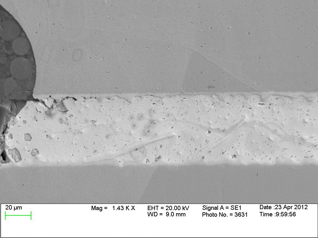
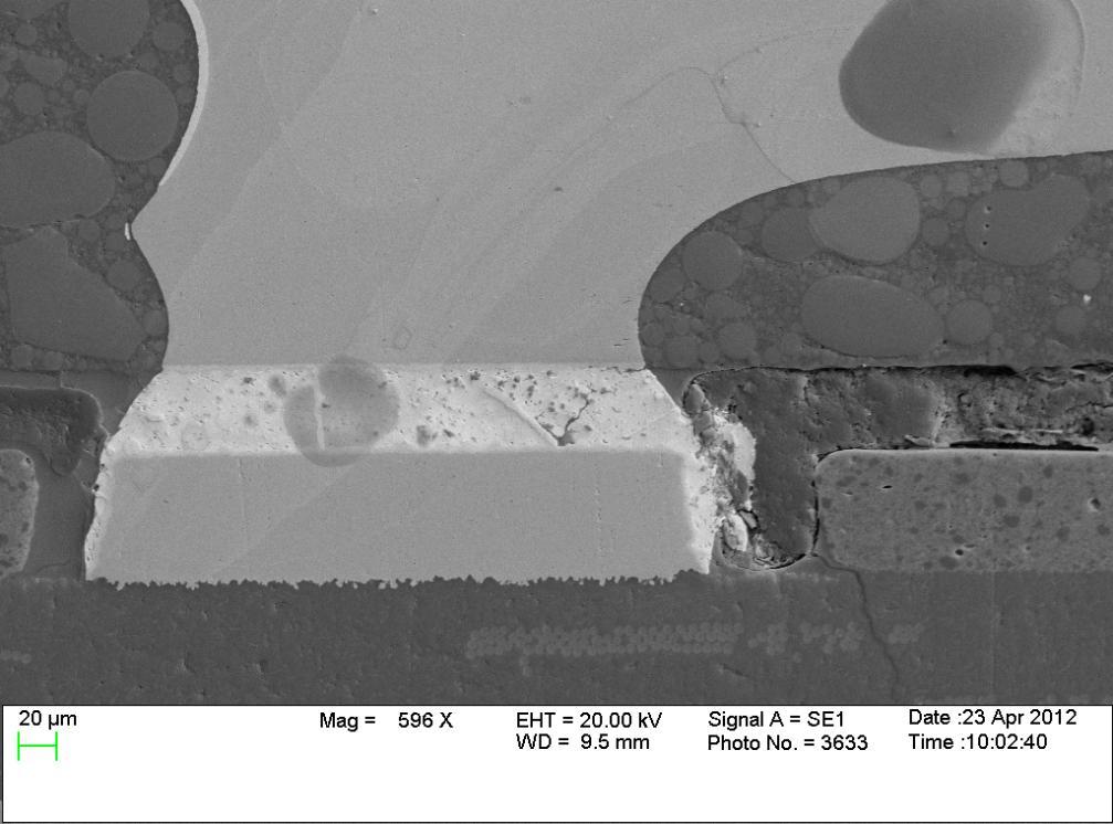
144 130
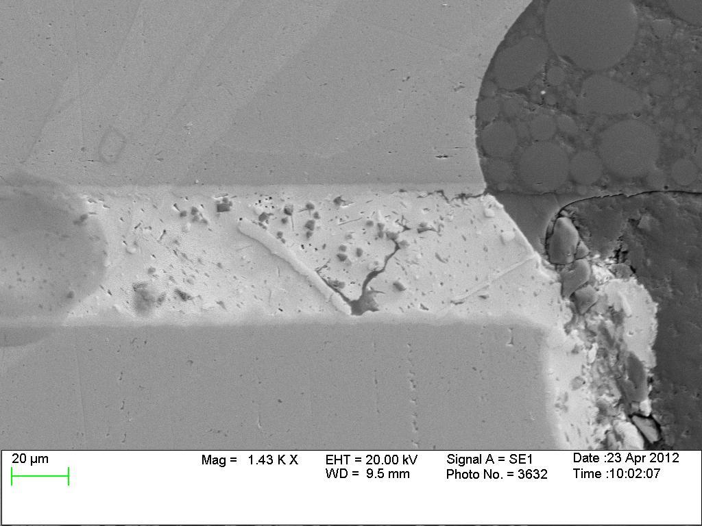
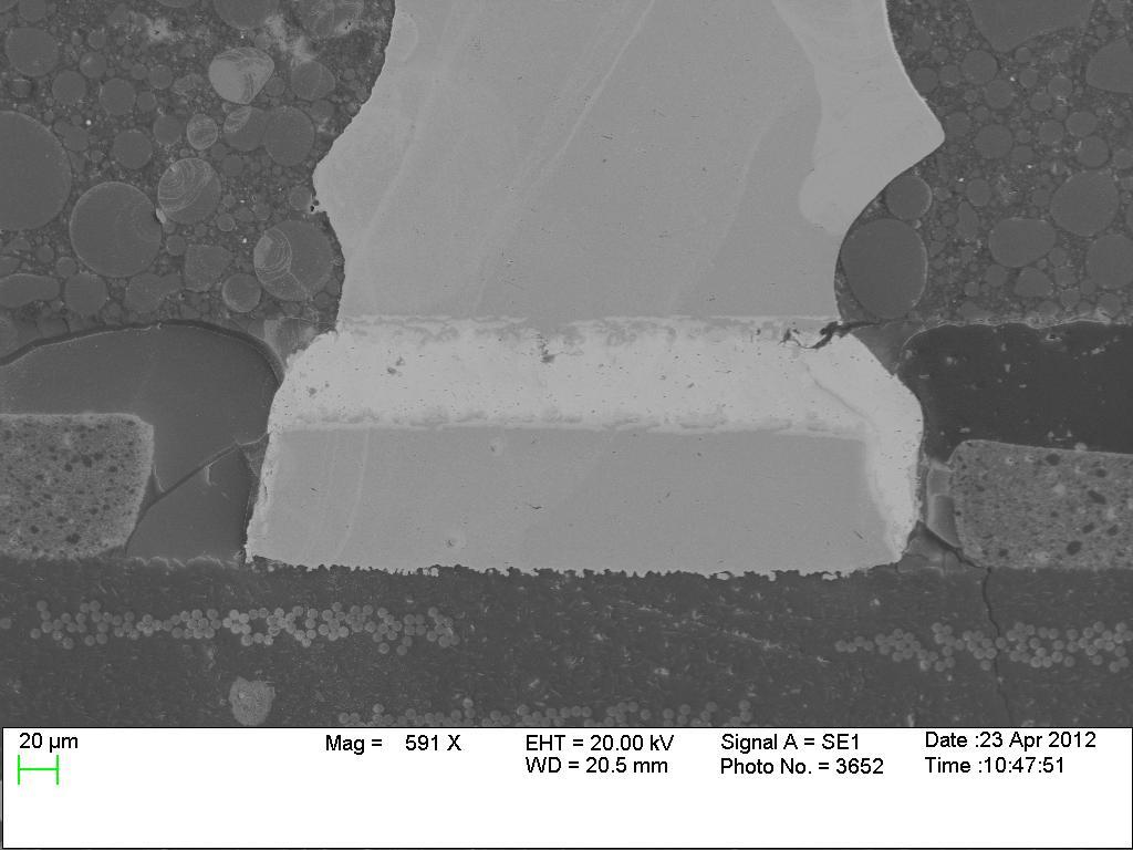
145 131


146 Figure 5.14 SEM microstructure of QFN at months 132
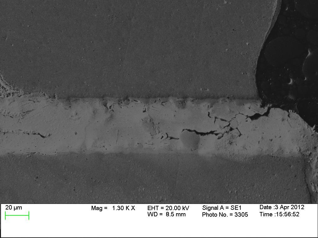
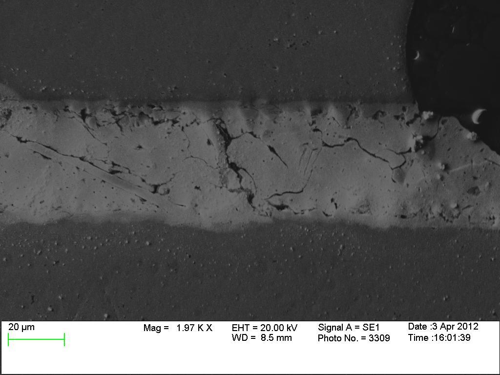
147 133
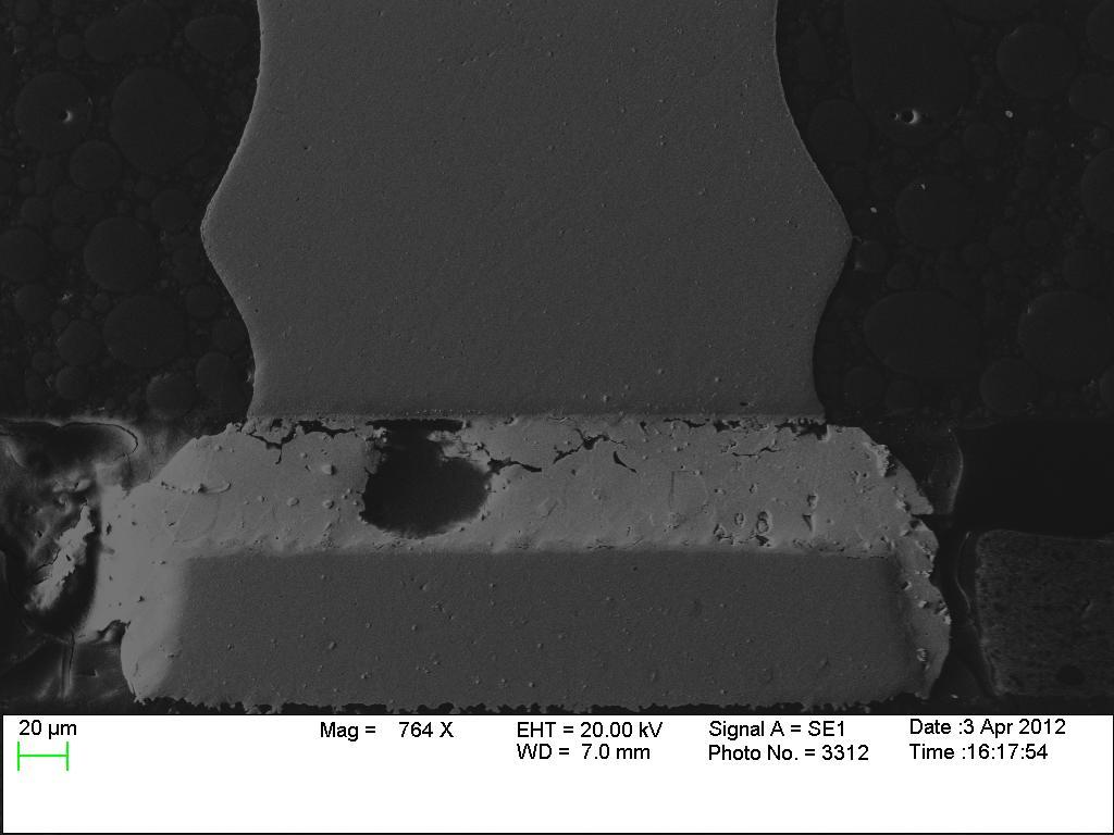
148 134


149 Figure 5.15 SEM microstructure of QFN at months Significant cycle lifetime degradation was observed for QFN after 12 months aging at 85 and 125. Failure analysis showed significant bulk Ag 3 Sn coarsening and intermetallic Cu 6 Sn 5 growth at the solder joint interfaces. And voids are also observed in the aging process for QFN components. 135