Review of CMOS Processing Technology
|
|
|
- Gerard Riley
- 5 years ago
- Views:
Transcription

1 - Scaling and Integration Moore s Law
2 Unit processes Thin Film Deposition Etching Ion Implantation Photolithography Chemical Mechanical Polishing
 - Vaporized material bombards onto substrate.")
3 1. Thin Film Deposition Layer of materials ranging from fractions of nanometer to several micro meters in thickness - Types of Thin Film Deposition Physical Vapor Deposition (PVD) - Vaporized material bombards onto substrate. Chemical Vapor Deposition (CVD) - Gaseous material reacts on substrate to form thin film
 Sputtering (DC, RF, Ion beam) Aluminum, Copper, Titanium, Tungsten")
4 1. Thin Film Deposition Physical Vapor Deposition (PVD) Evaporation (Thermal, E-beam) Sputtering (DC, RF, Ion beam) Aluminum, Copper, Titanium, Tungsten silicide
 PECVD (Plasma Enhanced) LACVD (Laser Assisted) MOCVD (Metal")
5 1. Thin Film Deposition Chemical Vapor Deposition (CVD) Gases react on the substrate to form the desired thin films LPCVD (Low Pressure) PECVD (Plasma Enhanced) LACVD (Laser Assisted) MOCVD (Metal Organic)
6 2. Etching Wet Etching Reactants Products Reaction -SiO 2 etching by HF -Si 3 N 4 etching by H 3 PO 4 - Si etching by KOH -Wet etching avoided if possible: hazard materials, undercut Film Semiconductor Solution

 Typical parallel-plate reactive ion etching")
7 2. Etching - Dry etching: chemical reaction with gases to eliminate desired material - RIE (Reactive Ion Etching), ICP (Inductive Coupled Plama), IBE (Ion Beam Etching) Typical parallel-plate reactive ion etching system.

8 3. Ion Implantation Ion implantation for doping: As, P for N-doping B for for P-doping
 No.")
9 3. Ion Implantation - Gas Source: Ionizes source gas - Acceleration by bias - Beam control by magnetic field Key Control Parameters: - Beam Currents (tens of A ~ tens of ma) No. of ions implanted - Implantation Energy (tens of kev ~ MeV) Depth of implantation - Thermal annealing is required after implantation
")
10 4. Photolithography Produces patterns by transferring mask patterns onto the substrate (Example: patterning of oxide/nitride thin film)
 - Masks are typically realized with direct e-beam")
11 4. Photolithography - Resolution mainly limited by of light UV Deep UV Extreme UV ( tens of nms) - Masks are typically realized with direct e-beam writing


12 5. Chemical Mechanical Polishing (CMP) Makes the wafer surface flat for better lithography Chemical Mechanical Planarization(CMP) combines chemical action with mechanical abrasion to achieve selective material removal through polishing


13 Schematic Layout Invertor Source Drain Gate Metal 1
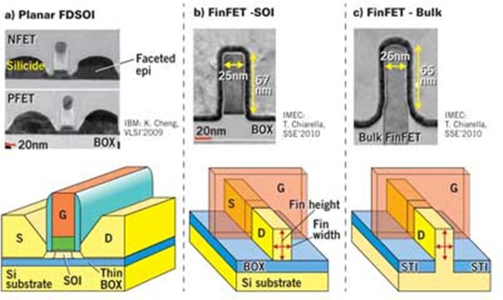
14 CMOS Structure Polysilicon Metal 1 Gate Oxide Dielectric SiN Spacer silicide P+ N+ STI N-well P-substrate

15 Shallow Trench Isolation(STI) Active region SiO Silicon dioxide P-substrate
16 Well Formation Active region Photolithography N-well Ion implantation P-substrate


17 Gate and Source/Drain Formation Gate Drain & Source Poly Silicon Thin Gate Oxide P+ N+ N-well Gate Oxide Formation Photolithography Ion implantation P-substrate


18 Contacts and Metallization Metal 1 Metal 1 Dielectric SiN Spacer silicide N-well P-substrate

19 CMOS Fabrication Result Polysilicon Metal 1 ThinGateOxide Dielectric SiN Spacer silicide P+ N+ STI N-well P-substrate
20 - CMOS Circuit Design Process
21 Design example: CMOS inverter Schematic Simulation (Synopsis HSPICE, Cadence SPECTRE) <Inverter schematic>
22 Layout (Cadence VIRTUOSO) Layout of mask patterns for photolithography
23 Rule Checking (Mentor CALIBRE, Synopsis HERCULES, Cadence ASSURA) - Layout vs. Schematic (LVS) Make sure layout is identical to schematic - Design Rule Checking (DRC) No design rules for a given process should be violated during layout - These rule checking must be satisfied before fabrication can start

24 Parasitic RC extraction (Synopsis StarRC)
25 Post Layout Simulation Pre-sim Po-sim Pre-sim Po-sim - Modify your design if needed
26 - Complicated Digital Circuit Design - Impossible to do transistor-level simulation - Impossible to layout by hands Behavior-level design using Hardware Description Language (Mentor ModelSim)

 -Auto Layout")
27 Review of CMOS Processing Technology - Automatic Gate-level Synthesis (Synopsis Design_Vision) -Auto Layout (Synopsis Astro)

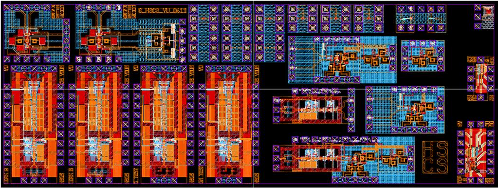
28 Example <Layout> <Fabricated chip>