Building new catalytic. plasma nanostructuring and large-scale synthesis of nanowires PlasmaLab
|
|
|
- Jacob Henry
- 5 years ago
- Views:
Transcription

1 Uros Cvelbar Jozef Stefan Institute, Slovenia Building new catalytic sensors and devices with plasma nanostructuring and large-scale synthesis of nanowires PlasmaLab F4-IJS


2 Sensors - Measurements of neutrals with nanostructured surfaces 1. Linear response 2. Wider operation range 3. Better correlation with O-atom density CVELBAR, et al. [also selected as a topical article for the Aril 14, 2008 issue of Virtual journal of nanoscale science & technology]. Appl. phys. lett., 2008, vol. 92, no. 13, str


3 Applications Nanowire array electrodes for electrochromics ission %Transm V V V Wavelength (nm) 70% % Transm mission FTO glass Electrolyte WO 3 nanowires FTO glass 700 nm 50% Time, Sec bleached colored


4 Applications Nanowire mat electrodes for electrochromics % Transmis ssion V V V Wavelength (nm) ssion FTO glass Electrolyte WO 3 nanowires 700 nm FTO glass 50% 33% % Transmi Time, sec Differences in the timescales of coloration and bleaching bleached colored
5 Problem to solve Synthesize large quantities of NW at small costs for satisfy future industrial needs! Winner processes: 1. Fast process 2. Cheap material in (powders) / out (NW) 3. Yield quantities 4. Efficient (and small) energy consumption 5. Pureness of material and new properties (crystallinity, p/n-type, etc.) 6. No post-processing, purification 3D problem: TIME QUANTITY- QUALITY
6 Time consumption for processing
7 Plasma routes Different plasma routes for nanostructuring ring and large scale synthesis of nanowires Separate NW to build in 1. Plasma-Enhanced Chemical Vapor Deposition (PECVD) 3. Plasma flight-thruthru Pre-deposited NW - electrodes 2. Plasma-Catalyst assisted 4. Direct Plasma synthesis 5. Mixed plasma routes Case of IRON OXIDE and ZINC OXIDE interest in sensors, solar cells, batteries or other photochemical and electrochromic applications
8 1. PECVD Evaporation/melting-plasma interactions-deposition Liu et al. Adv. Mater. 2005, 17, Ostrikov et al Thin Solid Films 516, Liu et al J. Appl. Phys. 95, Kumeta et al Thin Solid Films 518, Ono H et al Thin Solid Films 581, Baxter et al Appl. Phys. Lett. 83, Hong et al Phys. Plasmas 13, Hong et al 2006 Jpn. J. Appl. Phys. 47,


9 Fe3O4 NW 1.PECVD Hong et al Phys. Plasmas 13, ZnO NW Liu et al 2005 Adv. Mater., 17, Ostrikov et al Thin Solid Films 516, Liu et al J. Appl. Phys. 95, Kumeta et al Thin Solid Films 518, Ono H et al Thin Solid Films 581, Baxter et al Appl. Phys. Lett. 83,


10 2. Plasma-catalyst assisted Catalyst deposition plasma interactions NW growth Fe2O3 = O ZnO = book Inorganic nanowires and applications by M. Meyyappan, MK Sunkara


11 DC 3. Plasma flight-thru RF MW Ko TS et al 2006 Mater. Sci. Eng. B 134, Lin Hf et al 2009 J. Cryst. Grow. 311, Peng H et al 2007 J. Phys. Chem. C 111, Kumar V et al 2008 J. Phys. Chem. C 112, Kim JH et al MK 2008 Informacije Midem 38,
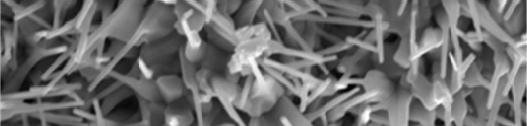
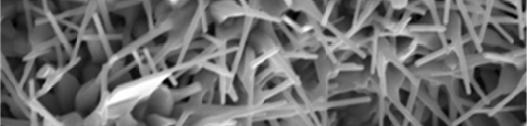


12 3. Plasma flight-thru ZnO Nanowires αfe2o3 Nanowires


 pp 00288y")


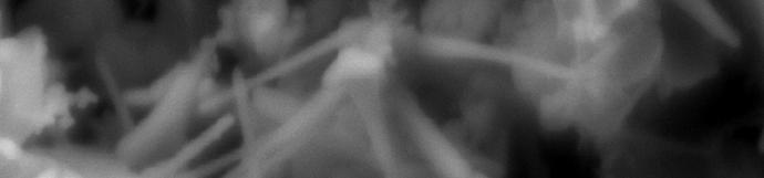
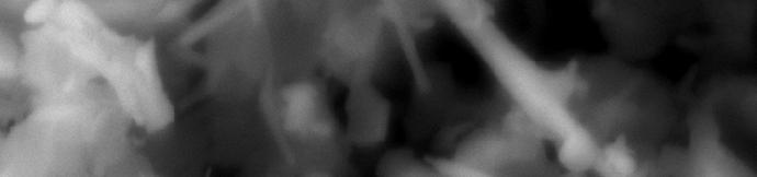
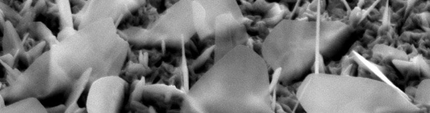
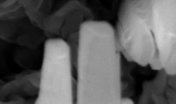
13 4. Direct plasma growth αfe2o3 Nanowires Chen, Cvelbar, Mozetic, Sunkara Chem. Mater. (2008) pp 00288y Cvelbar, Chen, Sunkara, Mozetic, 2008 Small 4, Cvelbar U and Ostrikov K 2008 Cryst. Growth 2 Des. 8, Ostrikov K, Levchenko I, Cvelbar U, Mozetic M and Sunkara MK 2010 Nanoscale 2, a) 3 µm b) Thermal 3 Plasma 4 4 µm


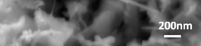
14 4. Direct plasma growth SELF-Nucleation 100nm 200nm


 b)")
15 4. Direct plasma growth ZnO Nanowires Sunkara Solid-solid d interface Cvelbar Solid-liquid interface a) b) Unpublished or hidden?
16 5. Mixed plasma routes Plasma-catalyst assisted + flight-thru Plasma-catalyst assisted + flight-thruthru + PECVD? Iron oxides? ZnO NW a) b)
17 Time vs. Quantity (Fe oxide)


 MW 5g/min, ration")
18 Time vs. Quantity (ZnO) 1. PECVD g/min 3. Plasma flight-thru DC g/min (Mat.Sci. Eng. B 134(2006) RF 20 g/min, ratio l/d=14 [optimal] 37 g/min, ratio l/d=8 53 g/min, ratio l/d=2 (J. Phys. Chem. C 111(2007) MW 5g/min, ration l/d=20 (J.Phys.Chem C (2008)) <20g/min (Midem Info 2008)
19 Time vs. Quantity (Zn oxide)
20 Quality Advanced properties of NW Pure structures / no impurities (in most cases) Dimensions, shapes, ratio l/d Process control


21 Advantages of plasma nanostructures Why is plasma so important for nanostructure or NW growth? - SUPERSTRUCTURE Superstuctured lattices (1/10 oxygen vacancies) grow only on plasma synthesize wires and not on thermal synthesized ones (furnace)! Potential, V vs. SCE n-type 1.5 nm Thermal p-type Time/s nm 1.5 Plasma
22 Prespectives & pros-cons 1. PECVD 2. Plasma catalyst assisted 1. Polycrystalline / crystalline NW 2. Aligned array growth is difficult to achieve 3. NW growth on substrate depends on the substrate 4. Multiple step procedures 5. Low energy efficiency per synthesized NW 1. Impure NW 2. Multiple step procedures 3. High temperatures needed for dissolvation of metal into catalyst for NW growth (e.g. 925C for Zn vapor dissolved into Au catalyst) 4. High energy consumption / low energy efficiency per synthesized NW 5. Growth limited by supplied catalyst 3. Plasma flight-thru 1. Single-crystalline NW 2. High amount of NW yield 3. Particles mixed with NW post-purification purification needed 4. Difficult to control NW shape and ratio length/diameter 5. Difficult to control morphology 6. Synthesis smaller than second 7. Influence of reactor size to feed and efficiency of conversion/syntheis 8. Single-step procedure 9. Good energy efficiency per synthesized NW 4. Direct plasma synthesis 1. Single-crystalline NW 2. Medium amount of NW yield 3. No purification needed 4. Good control of NW shape and ratio length/diameter 5. Difficult to control nucleation 6. Nucleation determines the number of NW 7. Difficult to control aligment of NW 8. Synthesis in order of seconds to minutes 9. Single-step procedure 10.Medium energy efficiency per synthesized NW