Simple Cubic Crystal
|
|
|
- Melanie Burns
- 5 years ago
- Views:
Transcription
1 Starting Material
2 Simple Cubic Crystal
3 Crystal Planes offset by d/4 Diamond lattice cell (C, Si, Ge, etc.) face atom in FCC corner atom in FCC (100) plane (110) plane (111) plane
4 Crystal Planes/Direction Direction [001] z 2 1 Indexing Procedure for Planes 1. Record where the plane intercepts the axes in the unit of the unit cell length. 3, 2, Plane (233) y 2. Invert the intercept values 1 / 3, ½, ½ x 3 3. Convert to the smallest possible set of whole numbers 2, 3, 3 Direction [100] 4. Enclose the whole-number set in parentheses (233)

5 Wafer Flat Wafer flats in 4 and 6 silicon wafers Newer wafers (8 and 12 ) now use a groove to mark the orientation, instead of a cut to save some area for test structures. Manufacturers Data of incoming wafers: Orientation, thickness, doping type, resistivity.
6 Resistivity and Mobility t Four Point Probe Sheet resistance : R s (Ω/ )= ρ(ω.cm) / t (cm) J drift = (qp μp +qn μn )F=σ F ρ = qnμ n 1 + qpμ p
7 Cleaning
8 Wafer Cleaning Contamination Possible source Effects Particles Metal Organic Need to remove the contaminations on wafer surface Microroughness Native Oxide Equipment, ambient, gas, Deionized (DI) water, chemical Equipment, chemical, reactive ion etching (RIE), implantation, ashing Vapor in room, residue of resist, storage containers, chemical Initial wafer material, chemical Low Ambient moisture, DI water rinse Low oxide breakdown field, Poly-Si and metal bridging-induced low yield (both open and short) Low breakdown field, Junction leakage, Vt shift, Reduced minority lifetime Change in oxidation rate oxide breakdown field Low mobility of carrier Degraded gate oxide, low quality of epi-film, high contact resistance, poor silicide formation

9 2007 ITRS Contaminants may consist of particles, organic films (photoresist), heavy metals or alkali ions. Modern IC factories employ a three tiered approach to controlling unwanted contaminants: 1. clean factories 2. wafer cleaning 3. gettering
10 13 Cleaning Steps in CMOS Brief Processes (Front-End) Wafer start Start oxide Zero layer N-well I/I define P-well I/I Well-drive in Etch oxide STI Sac oxide VT, N-apt P-apt Gate oxide Poly-Si N-LDD, p-ldd Spacer S/D thin oxide N + -S/D P + -S/D BPSG Contact etch


11 Polymer and Pillar Formation After metal etching, PR stripping, and metal remove After poly-si etch After contact hole SiO 2 etch
12 Oxide quality is strongly related to the wafer cleaning, which determines the yield, reliability, and performance of IC circuits Cleaning technology DI water Chemical equipment Chemical Impurity, metals Gate Oxide Integrity Wafer Si wafer technology Drying process Particles Cleaning recipe Roughness Gases Temp Oxidation technology
13 Cleaning Technology Wet Cleaning Immersion technique: bulky chemical solution Megasonic cleaning particles and contamination can be removed with dilute solution Centrifugal spray cleaning Cheaper & faster Dry cleaning Ultraviolet-ozone clean (UVOC) Effective in removing hydrocarbon HF/H 2 O vapor clean O 2 plasma cleaning Ar/H 2 plasma cleaning Thermal cleaning
14 Procedure of Wet Wafer Cleaning Wet cleaning = cleaning + rinsing + drying
15 Standard RCA Clean H 2 SO 4 : H 2 O 2 = 3 : 1 to 5:1 (Sulfuric-peroxide mixture, SPM) C for min. Dissolve heavy organic molecules Remove heavy metals HF : H 2 O = 1: 50 ( 1 min ) NH 4 OH : H 2 O 2 : H 2 O = 1 (0.05) : 1 : 5 (RCA-1, SC-1, APM) C for min. oxidize organic molecules Complex BI and BII metals (Cu, Au, Ag, Ni, Zn, Co, Cr etc) Remove particles (with megasonic) HCl: H 2 O 2 : H 2 O = 1 : 1 : 6 (RCA-2, SC-2, HPM) C for min. Remove alkali ions and Al 3+, Fe 3+, Mg 2+ ions, etc. by forming water solvable chloride complex (HF-last) Original RCA clean
16 Dependence of E bd Yield on Particle Density Particle concentration(number/ml) in ULSI-grade semiconductor chemicals 0.2um 0.5um NH 4 OH H 2 O HF HCl H 2 SO
17 Particle Adhesion & Removal Adhesion Static charge Van der Walls forces Electrical double layer Capillary action around the particle Chemical bond Removing Mechanism Dissolution Oxidizing degradation and dissolution Lift-off effect by slight etching of the wafer surface Electric repulsion
18 Deposition of Particles onto Wafer Surface as a Function of PH As a function of PH value H 2 O 2 consumes gradually with time
19 Metallic Contamination Impacts on yield Structural defects at the interface Stacking faults during later oxidation or epitaxial process Increased leakage current of p-n junctions Reduced minority carrier lifetime Adhesion mechanisms Direct binding : Au, Ag, Pt has higher electronegativity tending to neutralize by capturing electron from Si Incorporated in oxide during oxide formation : Al 2 O 3, Cr 2 O 3, CrO 2, Fe 3 O 4. Removal Converting metal into ions which are soluble in the solution Oxide removal

20 Metallic Removal + Si + 2H O SiO + 4H + 4 e (1) 2 2 z+ M M + ze (2) Oxidant/ Reductant Standard Oxidation Potential (volts) Oxidation-Reduction Reaction Mn 2+ /Mn 1.05 Mn Mn e SiO 2 /Si 0.84 Si + 2H 2 O SiO 2 + 4H + + 4e Cr 3+ /Cr 0.71 Cr Cr e Ni 2+ /Ni 0.25 Ni Ni e Fe 3+ /Fe 0.17 Fe Fe e H 2 SO 4 /H 2 SO H 2 O + H 2 SO 3 H 2 SO 4 + 2H + + 2e Cu 2+ /Cu Cu Cu e O 2 /H 2 O H 2 O O 2 + 4H + + 2e Au 3+ /Au Au Au e H 2 O 2 / H 2 O H 2 O H 2 O 2 + 2H + + 2e O 3 /O O 2 + H 2 O O 3 + 2H + + 2e The strongest oxidants are at the bottom (H 2 O 2 and O 3 ). These reactions go to the left grabbing e- and forcing (2) to the right. Fundamentally the RCA clean works by using H 2 O 2 as a strong oxidant.
21 Metallic Contamination Element Eletronegativity Half-cell Reduction potential Au Pt Ag Hg Cu Si Pb Sn Ni Fe Zn Tendency To be participated on bare Si Al Mg Ca Na K
22 Example of SPM clean Metallic Contamination
23 Metallic Contamination Ca 15nm SiO 2


24 Oxide Defect Density Versus Iron Contamination
25 Impacts on yield Organic Contamination Cause incomplete cleaning Adhesion mechanisms/sources Organic vapor in the ambient Container Photoresist Removal Dry ashing (O 2 plasma) SPM Ozone-injected water Lower temperature, simplicity, reduced chemical usuage
26 Surface Roughness Mainly caused in SC1 (SPM and SC2 won t) NH 4 OH acts as etchant of oxide H 2 O 2 acts as oxidants Surface roughness reduction Reduce proportion of NH 4 OH(the etchant) Reduce the temperature of the bath Reduce the cleaning time Be careful, the concentration of NH 4 OH can not be too low ( ; efficiency issue)

27 Today s Gate Dielectric SiO 2 density = 2.2 g/cm 3 1 layer of SiO 2 ~ 0.36 nm
28 Surface Roughness

29 Effect of Roughness on Electrical Properties


30 Native oxide: 1-2 nm Issues caused by native oxide Native Oxide Uncontrolled ultrathin oxide growth High contact resistance Inhibition of selective CVD or epitaxy Metal impurities are included in native oxide HF-last SPM

31 Contact Angle Surface of Si Surface of SiO 2 Hydrophilic surfaces are more easily wet by cleaning solutions and during drying any particles on the surface tend to stay in solutions until solution is removed from the surface Hydrophobic surfaces are more difficult to clean, cleaning solutions do not wet as well and during drying solutions tend to bead up on the surface Leaving the particles on the surface instead of keeping particles in the solution.


32 MOS Capacitor IV with and without Preoxide Preoxide: 300 o C in O 2 ;to prevent Si etch at high-temp


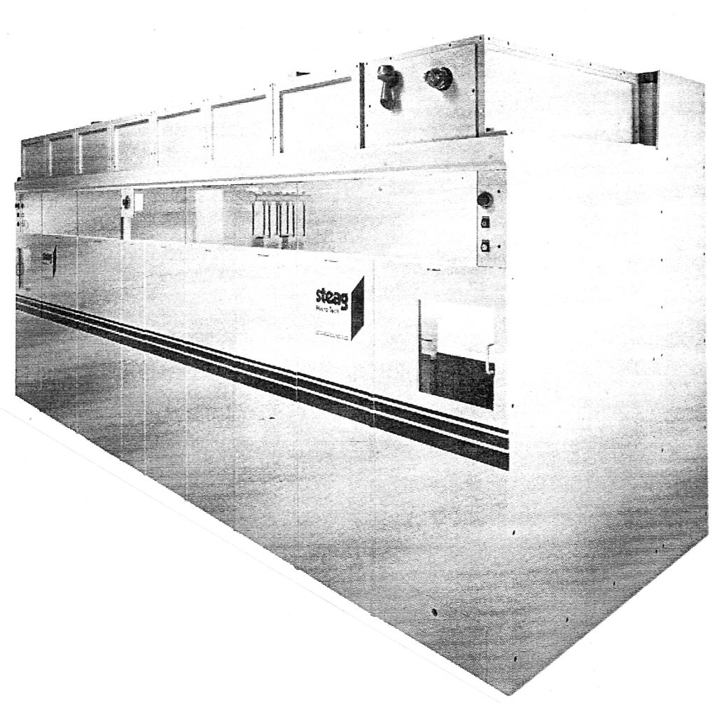
33 Wafer Cleaning Facility Wet Bench DI Water Tank

34 Conventional Wet Bench