Chapter 1. Introduction to Thin Film Technology
|
|
|
- Kimberly Blankenship
- 5 years ago
- Views:
Transcription
1 Chapter 1. Introduction to Thin Film Technology Thin films are deposited onto bulk materials (substrates) to achieve properties unattainable or not easily attainable by substrates alone. How thin? 1
2 Properties: Optical Electrical/ electronic Magnetic Chemical Mechanical Thermal Applications: Reflective/antireflective coatings; interference filters; decoration (color, luster); memory disks (CDs, DVDs); waveguides; displays; solar cells; photodetector arrays Insulation; conduction; semiconductor devices; piezoelectric drives; integrated circuits; solar cells; displays; photodetector arrays Memory disks Barriers to diffusion or alloying; protection against oxidation or corrosion; gas/liquid sensors Tribological (wear-resistant) coatings; hardness; adhesion; micromechanics Barrier layers; heat sinks 2
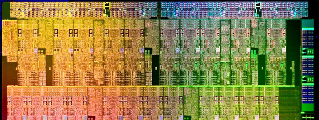
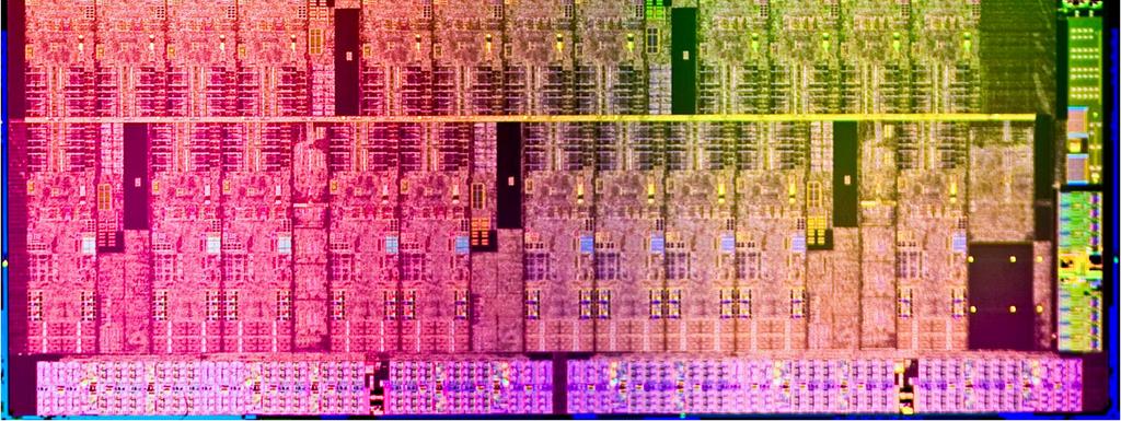
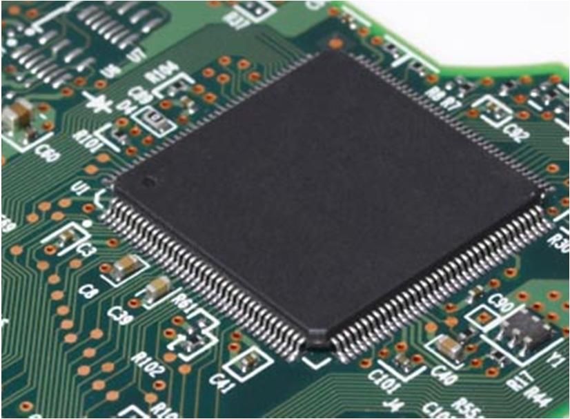
3 Integrated Electronic Circuits 3


4 Inside top Inside cross-section SRAM transistors in Apple s ipad 2 A5 4


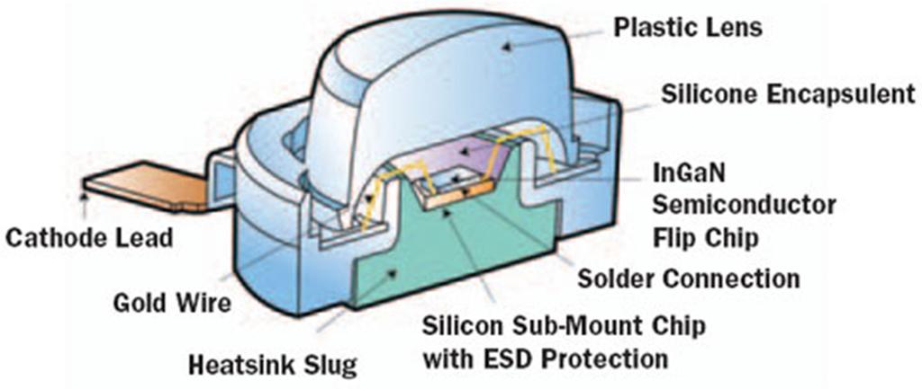
5 LED Arrays as Displays 5
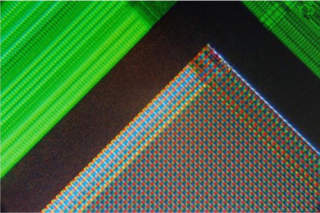
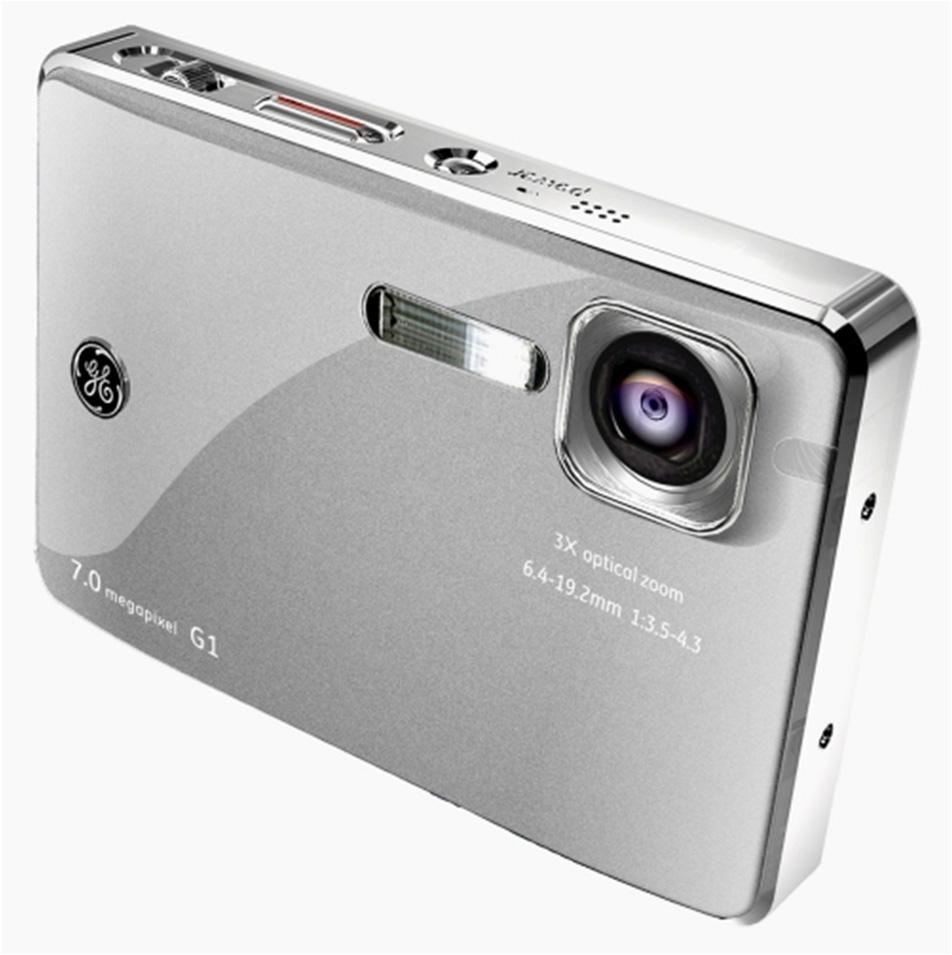
6 Photodetector Arrays in Digital Cameras 6

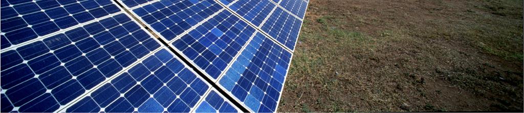
7 Solar cell plant 7


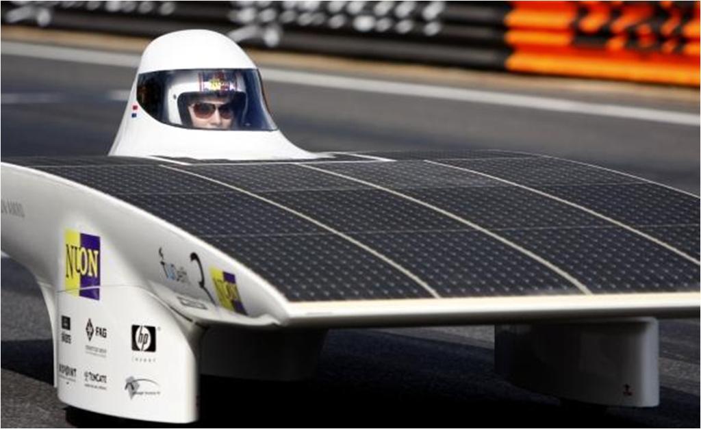

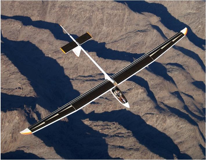
8 Cars and airplanes powered by photovoltaic devices
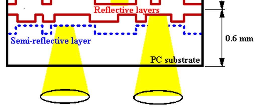
 780 nm Image of")


9 Recordable CD (CD R) 780 nm Image of the data zone on a CD-R Magnification: 32x Total track length: ~3 miles 9

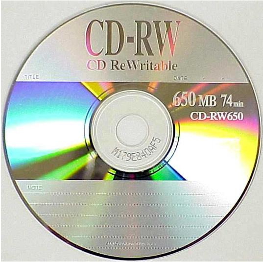
10 Rewritable CD (CD RW) 780 nm 10


11 DVD nm 11


12 DVD nm 12

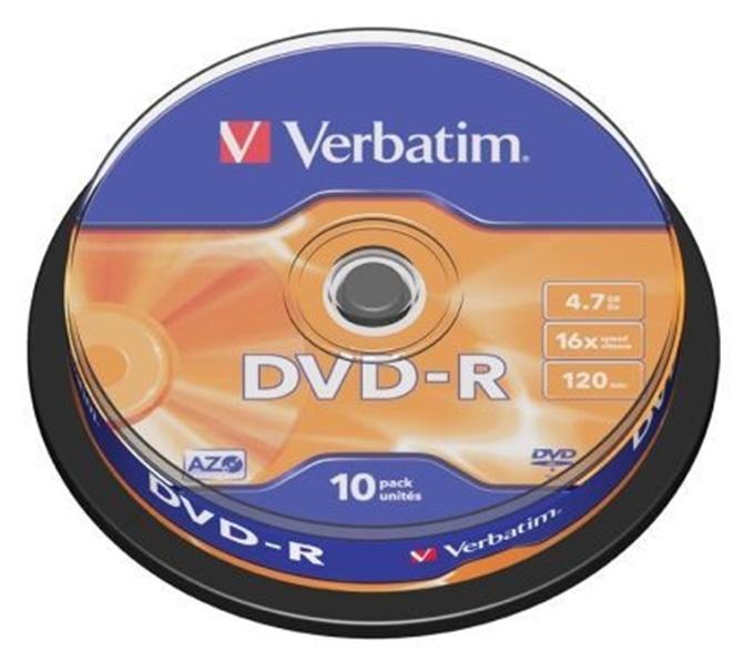
13 DVD nm 13


14 DVD nm 14

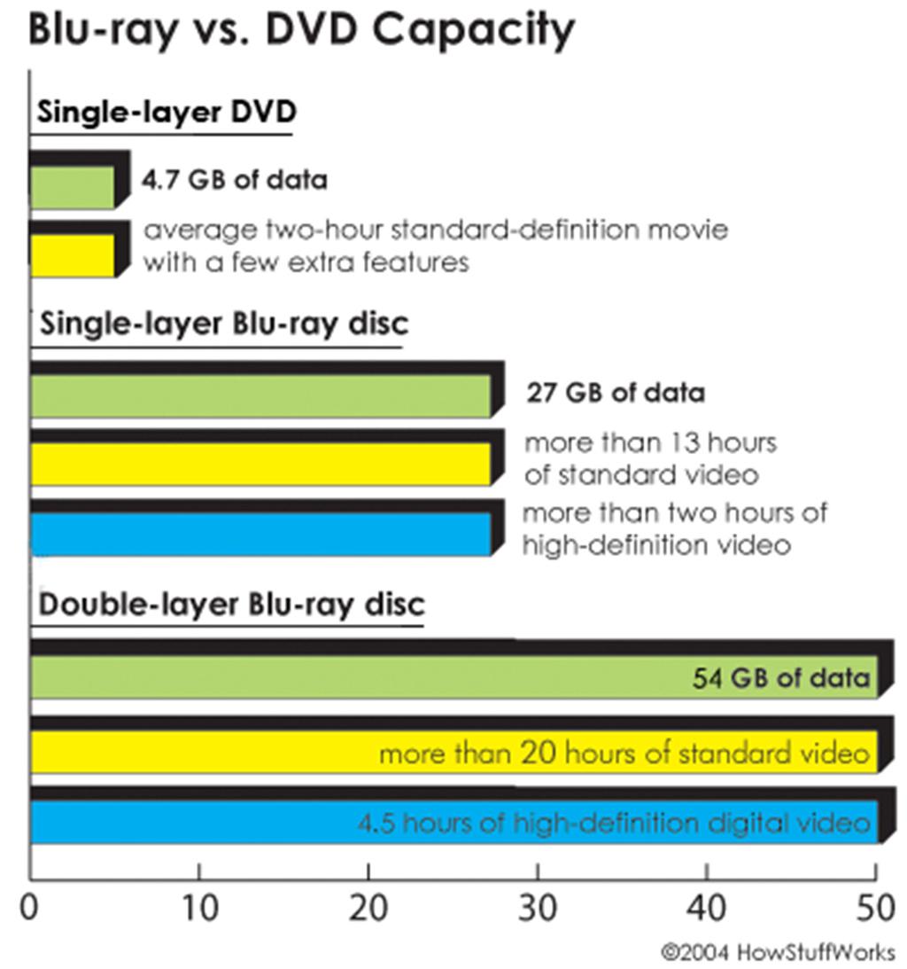

15 Blu ray Disc 405 nm 15

16 Blu ray Disc 16
17 Phase Change Alloys T g : crystallization temperature T m : melting temperature 17


18 Phase Change Alloys To write information, a short pulse of high-intensity laser beam locally heats the phase-change material above its T m. Rapidly cooling the alloy at rates > 10 9 K s 1 quenches the liquid-like state into a disordered, amorphous phase. To erase stored information, an intermediate-power laser pulse is used. The laser locally heats the film above its T g, where the atoms become increasingly mobile and can revert to the crystalline state, erasing the recorded information. 18
19 Phase Change Alloys Nat. Mater. 2007, 6,


20 Multilayer films of different materials Dielectric mirrors consist of multiple layers of films alternating between high and low indexes of refraction. A, B, and C waves are in phase with each other and interfere constructively. 20
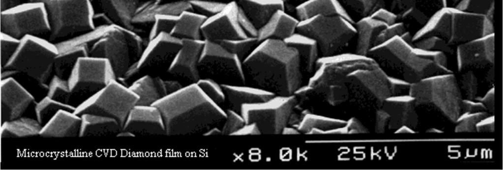
. A mean free path and coherence length on the order of 10 m insure that the carriers are coherent and ballistic.")
21 Semiconductor heterostructures 2D electron gas: Electrons are confined vertically to the ground state of a quantum well located at a GaAs/AlGaAs interface, and form a twodimensional electron gas (2DEG). A mean free path and coherence length on the order of 10 m insure that the carriers are coherent and ballistic. Metallic gates deposited by electron beam lithography confine electrons laterally. A number of interesting phenomena related to quantum Hall effect (both integer and fractional) have been discovered on this system. 21


22 Thin films for multiple properties Cr coatings on automobile parts Impart hardness, metallic luster, and protection against ultraviolet light. Cr coatings on plastic parts achieve the same functionality as the bulk metal but at significant savings in cost and weight. TiN coatings on cutting tools Offer hardness, low friction, and a chemical barrier to alloying of the tool with workpieces. 22


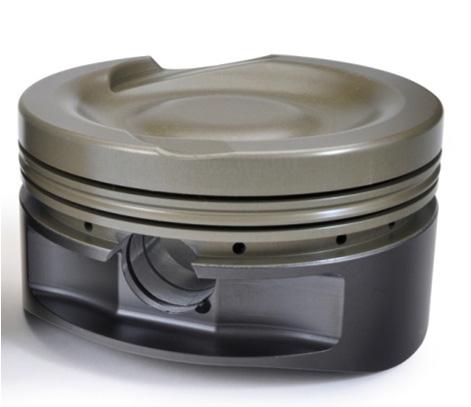
23 Coatings for prevention from corrosion 23

, and radio (3 khz 300 GHz,")

24 Stealth aircraft: employing a combination of technologies to reduce visibility in the visual, infrared (700 nm 1 mm), audio (20 Hz 20 khz), and radio (3 khz 300 GHz, for radar) frequency spectral regions. F-117A Nighthawk 歼 20 B-2 Spirit Stealth Bomber 24


25 歼 20 Perfect black carbon nanotube coatings make things invisible. 25
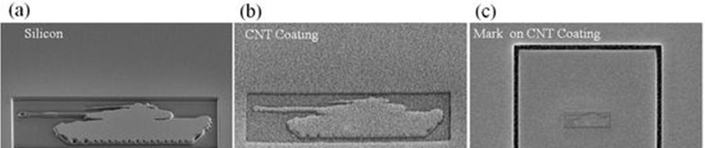
26 歼 20 26
27 Two more examples closer to current research: Diamond films and wafers Metallic quantum wells 27

28 QMWG800 Synthetic Diamond HPHT Hydraulic Cubic Press 28
 than any other material; (3) One of the highest resistivities ( > 10 16 cm) when no impurities are present; (4) Very high thermal conductivity ( = 1100 W m 1 K 1 ) exceeding those of Cu and Ag;")
29 Diamond films In addition to its unmatched beauty, diamond has a number of other remarkable properties: (1) Hardest substance ever known (H v > 8000 kg mm 2 ); (2) Higher elasticity modulus (E = 1050 GPa) than any other material; (3) One of the highest resistivities ( > cm) when no impurities are present; (4) Very high thermal conductivity ( = 1100 W m 1 K 1 ) exceeding those of Cu and Ag; (5) Low thermal expansion coefficient ( = K 1 ) to yield high resistance to thermal shock; (6) Resistance to chemical attack. These facts have spurred exciting and competitive quests in materials science: the preparation of diamond. The most common method for depositing diamond films is chemical vapor deposition (CVD). 29

30 30
31 31


32 Nonstick pan Medical implants Piston Part in AK47 rifle 32
33 Diamond wafers Diamond can also be an outstanding semiconductor material, superior in many ways to silicon. Diamond devices could operate at higher temperatures (>400 C) and higher power than those of silicon, as well as being faster, denser and more resistant to radiation. But practical diamond electronics will need large-area, single-crystalline diamond wafers to be fabricated, analogous to silicon wafers commonly used in the semiconductor industry. Diamond can be grown on diamond (homoepitaxy) by chemical vapor deposition. Electronics-grade diamond has been made in this way. But single-crystal diamond substrates are small and expensive. The alternative is to grow diamond on a foreign (non-diamond) single-crystal wafer (heteroepitaxy). 33


34 Comparison between Diamond and Silicon 34
35 Room-temperature drift mobilities of 4500 cm 2 V 1 s 1 for electrons and 3800 cm 2 V 1 s 1 for holes have been measured in high-purity single-crystalline diamond. Such high charge mobilities of single-crystalline diamond films are encouraging for the development of high-performance diamond electronics. J. Isberg, J. Hammersberg, E. Johansson, T. Wikström, D. J. Twitchen, A. J. Whitehead, S. E. Coe, G. A. Scarsbrook, Science 2002, 297,
 and temperature (2500 2800 K). The superconducting transition temperature T c is ~4 K. E. A.")
36 Superconductivity in diamond Boron is relatively easily doped into diamond as a charge acceptor. Superconductivity has been discovered in B-doped diamond synthesized at high pressure (nearly 10 5 atm) and temperature ( K). The superconducting transition temperature T c is ~4 K. E. A. Ekimov, V. A. Sidorov, E. D. Bauer, N. N. Mel nik, N. J. Curro, J. D. Thompson, S. M. Stishov, Nature 2004, 428,


37 Epitaxial Growth Nature 2003, 424, 500; Science 2008, 319,

38 Pb Films Grown on Si Substrates Science 2004, 306,
39 Superconducting T c Changes 39
40 This course will focus on the deposition of thin films from the vapor phase. Omitted will be the deposition of thin films from the liquid phase and films grown by reaction with the substrate rather than by deposition, such as SiO 2 grown by the thermal reaction of water vapor with Si. Vapor phase thin-film techniques have three advantages: (1) applicability to any material, (2) wide adjustability in substrate temperature, and (3) access to the surface during deposition. Liquid-phase techniques, such as electroplating, are useful for low-cost production. However, they are more related to chemistry instead of physics. 40

41 A typical Thermal Evaporation System 41
42 Process Steps Solid materials are vaporized by heat or by an energetic beam of electrons, photons (laser ablation), or positively ions (sputtering) in order to transport them to substrates. These methods are categorized as physical vapor deposition (PVD). Thin-film processes that use gases, evaporating liquids, or chemically gasified solids as source materials are categorized as chemical vapor deposition (CVD). 42
43 A major issue in the transport step is the uniformity of the arrival rate over the substrate area. In a high vacuum, molecules travel from the source to the substrate in straight lines, whereas in a fluid there are many collisions among molecules during the transport step. Therefore, in a high vacuum, the uniformity is determined by the geometry, whereas in a fluid it is determined by gas flow patterns and by the diffusion of source molecules through other present gas molecules. Substrate surface conditions include roughness, contamination level, degree of chemical bonding with arriving materials, and crystallographic parameters. The reactivity factor refers to the probability of arriving molecules reacting with the surface and becoming incorporated into the film. The probability is known as the sticking coefficient, S c. It can vary from unity to less than Energy input (substrate heating, photons, plasma, chemical reaction) has profound effects on both the reactivity of arriving materials and on the composition and structure of films. 43
44 Contents 1. Introduction to thin-film technology 2. Vacuum science and technology 3. Evaporation 4. Deposition 5. Epitaxy 6. Chemical vapor deposition 7. Film analysis 8. Physical properties of thin films 44
45 Reference Chapter 1. Thin-Film Technology in Thin-Film Deposition: Principles & Practice. 45