Equipment and Process Challenges for the Advanced Packaging Landscape
|
|
|
- Roxanne Johnston
- 5 years ago
- Views:
Transcription


1 Equipment and Process Challenges for the Advanced Packaging Landscape Veeco Precision Surface Processing Laura Mauer June Copyright 2018 Veeco Instruments Inc.
2 Outline» Advanced Packaging Market Landscape» Packaging Concepts and Equipment Challenges» Approaches and Examples» Summary 2 Copyright 2018 Veeco Instruments Inc.

3 Advanced Packaging Landscape - Markets 3 Copyright 2018 Veeco Instruments Inc.

4 Moore s Law Moore s Law and More than Moore Analog/RF Passives Power MEMS/ Sensors LED BioChips 130nm Si SiC GaAs Sapphire Ge 90nm 65nm CMOS Market Based Roadmap Chip Functions and Applications 45nm NVM Heterogeneous Integration 32nm 22nm 14nm SOI FinFET Scaling Roadmap and beyond 4 Copyright 2018 Veeco Instruments Inc.


5 3D High Performance Devices Require TSV Hybrid Memory Cube (HMC) High Bandwidth Memory (HBM) High End Graphics 5 Copyright 2018 Veeco Instruments Inc.

, through glass vias (TGV) or through organic vias (TOV),")

6 2.5D Interposers for Heterogeneous Integration A configuration where dies are mounted side by side on one side of a thin (~ 100 um) silicon, glass, or organic interposer using through silicon vias (TSV), through glass vias (TGV) or through organic vias (TOV), respectively through the interposer to connect the dies with the package substrate. Xiinx s Virtex 7 FPGA 6 Copyright 2018 Veeco Instruments Inc.
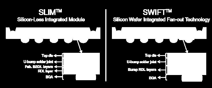
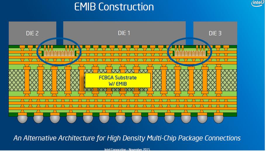
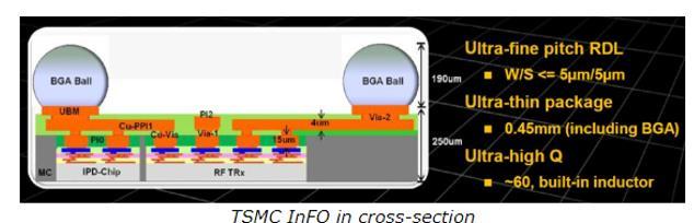
7 Other Technologies for Heterogeneous Integration Amkor TSMC Intel 7 Copyright 2018 Veeco Instruments Inc.

8 Wafers / Panels / Sizes for Advanced Packaging Source: Yole 8 Copyright 2018 Veeco Instruments Inc.

9 Panel Size Uncertainty for Large Area Fan-Out Source: TechSearch International 9 Copyright 2018 Veeco Instruments Inc.

10 Dimensions and Cost 10 Copyright 2018 Veeco Instruments Inc.


11 Advanced Packaging Options Package Max Size <15mm> Substrate Form Factor Wafer/Panel 300/330/450/500+ Materials Si/Glass/Organic Performance CTE Cost Bandwidth Performance Yield Chip Placement 2D/Stacked/Embedded Dimensions Line/Space Via/Pitch # I/O per mm 11 Copyright 2018 Veeco Instruments Inc.


12 Equipment and Process Flexibility for Advanced Packaging Options Substrate Handling Wafer/Panel Size Bow/Warp/Thickness Chemistry Selectivity for Materials Recirculation Replenishment Cost Cleanliness Debond Clean Post Dice Clean Process Control Endpoint Detection Profile Match For Uniformity 12 Copyright 2018 Veeco Instruments Inc.
13 Chemistry Example: Wafer Thinning 13 Copyright 2018 Veeco Instruments Inc.


14 Requirements for 2.5D and 3D Wafer Thinning Applications TSV Reveal FOWLP Si Etch for TSV Reveal: No etch of SiO2 liner or Cu TSV Fast Si etch rate Smooth surface finishing Good etch uniformity Cost effective Si Etch for FOWLP: Compatible with materials present in package structure such as Cu, Ti/TiW, SiO2, Si3N4, PI, and PBO Fast Si etch rate Good etch uniformity Cost effective 14 Copyright 2018 Veeco Instruments Inc.
15 Silicon Wet Etch Options > KOH (Potassium Hydroxide)» Good etch rate and selectivity (Silicon to Oxides /Cu)» Ionic contamination (K+) > TMAH (Tetramethyl Ammonium Hydroxide)» Safety concerns (toxicity) at high concentration» Slow etch rate > HF / Nitric based chemistry Spinetch» High etch rates but poor selectivity (Silicon to Oxides /Cu) > SACHEM Reveal Etch» Lower toxicity than TMAH» Higher etch rate and good selectivity (Silicon to Oxides /Cu) 15 Copyright 2018 Veeco Instruments Inc.


16 Etch Selectivity > Ability to etch silicon and stop on a variety of materials without causing damage * Spinetch D 1:6:2:1 HF:Nitric:Phosphoric:Sulfuric 16 Copyright 2018 Veeco Instruments Inc.
17 Two-Step Etch Process Developed > Step 1» Spinetch D (HF / Nitric mixture)» To smooth surface and eliminate grind marks» Contour silicon thickness for improved uniformity > Step 2» SACHEM Reveal Etch (or ST2011)» Selective etch of silicon» TSV oxide liner and Cu via» Other materials present at end of silicon etch for FOWLP 17 Copyright 2018 Veeco Instruments Inc.

18 Speed Wafer Center Etch Uniformity > Post Grind non-uniformities can have radial dependence» Center to edge variations Motion Profile Arm Motion > Single wafer etch process can compensate for radial nonuniformities» More/Less etch in center of wafer Post Grind Position on Wafer Dwell Time > Resulting Silicon wafer thickness is more uniform Post Etch 18 Copyright 2018 Veeco Instruments Inc.


19 Integrity of Via and Oxide Liner for TSV Reveal 19 Copyright 2018 Veeco Instruments Inc.
 caused damage to underlying RDL structure")


20 FOWLP Silicon Etch Results Strong Alklaine Etch (TMAH) caused damage to underlying RDL structure Use of acid etch or 2 step etch process provides good results with no damage to underlying structure High Density TSV-Free Interposer (TFI) Packaging with Submicron Cu Damascene RDLs for Integration of CPU/GPU and HBM IME presentation at ECTC Copyright 2018 Veeco Instruments Inc.
21 Process Control: Etch and Undercut 21 Copyright 2018 Veeco Instruments Inc.


22 UBM/RDL Etch and Dimensions > Smaller bumps with increased density > Need for less undercut and controlled etch» PSP WaferChek Process Monitor for endpoint detection > Recent demonstration on 10 and 20µm pitch bumps Current Products Future 22 Copyright 2018 Veeco Instruments Inc.

23 UBM Etch smaller bumps and higher density 23 Copyright 2018 Veeco Instruments Inc.


24 RDL Etch Pattern Density Challenges Isolated and Dense Features Embedded structures 24 Copyright 2018 Veeco Instruments Inc.

25 Undercut and Overetch > Isotropic etch results in undercut equal to thickness of film if etch stopped at endpoint > For narrow Line/Space dimensions undercut must be minimized» Reduce Thickness of seed layer» Eliminate / Reduce overetch 25 Copyright 2018 Veeco Instruments Inc.


26 WaferChek In-Situ Process Control for Endpoint Detection UBM Etch : Cu Over TiW Cu Etch TiW Etch Process Requirements Completely etch away field metal (barrier and seed metals) Plated Bump Keep overetch to a minimum for bump integrity, electrical performance and throughput No substrate attack Low Cost - $/wafer processed 26 Copyright 2018 Veeco Instruments Inc. 26

27 Undercut and Etchant Selection 27 Copyright 2018 Veeco Instruments Inc.
 Etch Example 28 Copyright 2018 Veeco")
28 Quantifying the Impact of Over-Etch on WPY Under Bump Metallization (UBM) Etch Example 28 Copyright 2018 Veeco Instruments Inc.
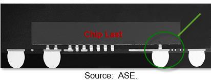
29 29 Copyright 2018 Veeco Instruments Inc. Substrate Handling Example: Cleaning on Film Frame


30 Cleaning Wafers on Film Frames post debond from carrier Larger than 300mm wafer ~380mm Removing residual adhesive without affecting tape film frame combination of appropriate chemistry and physical force 30 Copyright 2018 Veeco Instruments Inc. 30


31 Removing thick layer of adhesive without damage 31 Copyright 2018 Veeco Instruments Inc.
32 Cleaning post debond on film frames > Fixturing to handle and support wafer on film frame > Chemistry for cleaning/stripping residual and compatible with tape > Use of physical force (high pressure spray / high velocity spray) to assist in cleaning 32 Copyright 2018 Veeco Instruments Inc.
33 Summary > No single road being followed for Advanced Packaging > Many different types of packages depending upon application requirements > Equipment flexibility and versatility will be needed to address» Substrate size and form factor» Shrinking dimensions» Materials > Process solutions combine equipment and chemistry 33 Copyright 2018 Veeco Instruments Inc.

34 34 Copyright 2018 Veeco Instruments Inc. Thank you