Mikrosensorer. Microfabrication 1
|
|
|
- Iris Doyle
- 5 years ago
- Views:
Transcription
1 Mikrosensorer Microfabrication 1 Literature Introductory MEMS Fabrication and Applications Thomas M. Adams and Richard A. Layton Available as ebook on This lecture chapters (2) 3 & 4 MEMS Litography 1
2 Sensor fabrication Silicon manufacturing Litography Doping Etch techniques What is a micro sensor? A sensor with at least one dimension less than a millimeter 2
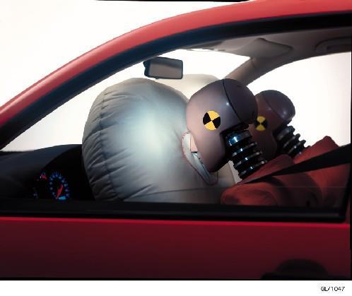

3 Accelerometers Inclinometer Gyro Compass Air bag sensor 3

4 Micro sensors Mechanical sensors Acceleration, pressure, angle Thermal sensors Temperature, flow, acceleration Magnetic sensors Digital compass, flow, position Optical sensors Absorbance, fluoroscence, position Chemical sensor / Biosensors / Gas sensors 4

5 Why micro sensors? Small Fast Low energy consumption Batch processing No material fatigue or hysteresis in silicon Polymer technology Laminar flow 5


6 Why not? Packaging o Mounting o Bonding o Sealing Signal out Energy supply MEMS Micro Electric Mechanical Systems Bulk Micromachining Surface Micromachining (Thin Film Technology) 6

7 Material Glass, quartz chemical sensors Polymers Single use Metals, Ceramics, Biomaterials Semiconductors - Silicon Czochralskiteknik 7

8 Czochralskiteknik Segregation Coefficient: k 0 =C S /C 1 C s = dopant concentration in the crystal C l = dopant concentration in the melt C 0 = original dopant concentration in the melt dopant concentration vs. Used melt Float zone teknik 8
9 Float zone teknik dopant concentration for multiple float zone passes Czochralski Float zone Starting material Molten polysilicon Most common method 90 % of all monocrystalline silicon ton per year Less pure silicon than with FZ Crucible contaminates with O 2 Starting material Poly silicon rod Less common 10% of world production Very pure silicon Successive purification 9
10 Öronmärkning av kisel Litography 10
11 Spin coating Litography 11

12 Positive photoresist Photo resists Negative photoresist Inverted photoresist 12


13 µ µ µ Permanent resists SU-8 Polyimide A 5µm wide, 500µm long isolated structure in 75µm thick resist 13

14 Lift-off Litography processes UV-litography Electron beam litography X-ray litography Ion beam- litography DWL LIGA 14

15 Litography processes Direct Writing Techniques Shadow projection High resolution Wear out the mask Lower resolution Longer lasting mask Resolution : 15
16 Resolution of Proximity litography Fresnel diffraction limits the resolution and minimum feature size to ~5µm Projections litography 16


17 Projections litography The mask is exposed in small portions ==> Better resolution ( 1 µm) than exposure of the entire mask Double sided litography 17
18 Intensity profiles for different litography methods Litography 18

19 Silicon dioxide Fabrication Wet oxidation H 2 +O 2 Water vapor 1000 C C Gasfasdeponering (CVD) Silicon dioxide Usage Mask layer Insulator Sacrificial layer Since the silicon dioxide lattice is much larger, thicker layers may induce stress in the material 19

20 Doping Deposition followed by thermal diffusion Most used method Solid phase deposition Gas phase deposition Thermal diffusion limits the resolution Ionimplantation; High concentrations Etching Techniques 20


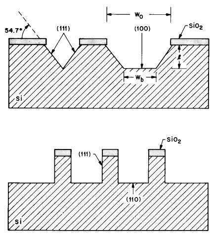
21 Isotropic / Anisotrop etch Anisotropic coefficient A f = 1- L H f Isotropic etching 21
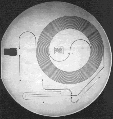
22 Standfordkromatografen 1978 Anisotropic wet etch 22

23 Silicon unit cell Silicon unit cell 23
24 Nearest neighbours <111> - silicon <100> - silicon Stop etch plane {111} 24
25 Crystal plane projection <100>-silicon Crystal plane projection <100>-direction 25

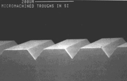
26 Anisotropic etch in <100>-silicon Anisotropic etch in <100>-silicon 26


27 Micro vials Masking of <100>-silicon 27

 EDP TMAH")
28 Underetch of <100>-silicon Before Underetching is finished Underetch of a random mask Freehanging structures over a V-trench Etch solutions Isotropic HNO 3 :HF:CH 3 OOH Anisotropic KOH (+IPA) EDP TMAH Hydrazine 28
29 Anisotropic etch KOH/water (isopropyl alcohol) Standard: 40 g KOH ml H 2 O 80 C Etch rate 1-2 µm/min Reduced surface roughness at higher concentrations SiO 2 etch mask is etched faster in a higher concentration Sticking of H 2 bubbles reduced by agitation (e.g. ultrasonic) Incompatible with IC (electronics) fabrication Etch rate in KOH 29
30 Anisotropy for various etch solutions KOH EDP TMAH Etchrates in different directions are exponentially dependent on the temperature, with different proportionality coefficients for different directions Trenches etched in (100)-silicon Etchrate for (100) and (110) plane change places when etch solutionchanges from KOH to EDP 30


31 Trenches etched in (100)-silicon for alignment of optical fibers Chip integrated optic cuvet 31

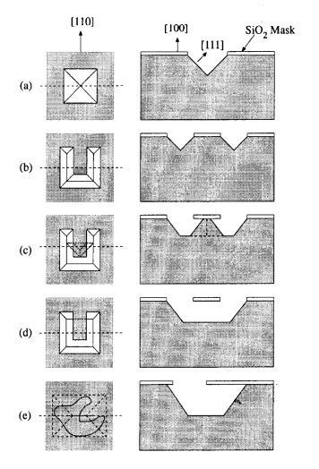
32 Anisotropic etching of convex structures 32
33 33