Deposition of niobium and other superconducting materials with high power impulse magnetron sputtering: Concept and first results
|
|
|
- Jesse Victor Dorsey
- 5 years ago
- Views:
Transcription

1 15th International Conference on RF Superconductivity July 25-29, 2011, Chicago Deposition of niobium and other superconducting materials with high power impulse magnetron sputtering: Concept and first results André Anders*, Rueben J. Mendelsberg, Sunnie Lim, Matthijs Mentink, Jonathan L. Slack, and Joseph G. Wallig, Lawrence Berkeley National Laboratory, Berkeley, California, U.S.A. Alexander V. Nollau, University of the German Armed Forces, Neubiberg, Germany Georgy Yu. Yushkov, High Current Electronics Institute, Tomsk, Russia * aanders@lbl.gov This work was initially supported by an LDRD grant of Lawrence Berkeley National Laboratory, and by the Office of High Energy Physics, U.S. Department of Energy, under Contract No. DE-AC02-05CH11231.
2 Nb-coated SRF Cavities: The promise of very substantial savings bulk Nb cavities are very expensive so far mixed results for sputtered films adhesion issues on copper relatively low RRR a proven technology for up to about 10 MV/m but Q 0 -slope at high field Breakdowns observed even at relatively low field Nb films on copper were demonstrated and utilized: LEP (CERN, 1996): 216 cavities with sputtered Nb, 6 MV/m with Q 0 = 3.4 x 10 9 at 4.5 K best sputtered Nb films on electropolished Cu cavities Fig. 4 of C. Benvenuti et al., Physica C: Superconductivity 351, 421 (2001).
3 Magnetron Sputtering Concept for Nb (1990s) Nb tube to be sputtered J. Langner, et al., 5th Int. Conf. on Modification of Materials with Particle Beams and Plasma Flows, Tomsk, Russia, 2000, pp


4 Thorton s Structure Zone Diagram Contains the effects of energetic particle bombardment J. A. Thornton, J. Vac. Sci. Technol. 11, 666, 1974

5 Generalized Structure Zone Diagram including the Effects of Plasma Assistance on Films ( Energetic Condensation ) derived from Thornton s diagram, 1974 T* = normalized temperature and potential energy t* = normalized film thickness E* = normalized kinetic energy A. Anders, Thin Solid Films 518 (2010) 4087


 A. Anders, Surf.")
6 HIPIMS: A Form of Ionized Sputtering. One Approach to Energetic Deposition. What distinguishes HIPIMS from the long-practiced pulsed sputtering? Technical Definition: HIPIMS is pulsed sputtering where the peak power exceeds the average power by typically two orders of magnitude. (implies a long pause between pulses, hence the term impulse ) about 500 kw peak 15 cm dia. Cu target Physical Definition: HIPIMS is pulsed sputtering where a very significant fraction of the sputtered atoms becomes ionized. (implies that self-sputtering occurs, which may or may not be sustained by target ions) A. Anders, Surf. Coat. Technol. 205 (2011) S1. image from the seminal (but not first) paper: V. Kouznetsov, et al., Surf. Coat. Technol. 122 (1999) 290 Why do we care? Because bias can be applied to affect film-forming ions (not atoms)!


7 Metal Plasma Generator: High Power Impulse Magnetron Sputtering Copper target 2 magnetron A. Anders, et al., JAP 103 (2008)
 S1.")
8 substrate ions to substrate atoms to substrate Probability for ion to return to target β secondary electron yield γ SE target α sputter yield γ Ionization probability Condition of selfsputtering runaway Π αβγ> 1 Condition of steady-state self-sputtering Π αβγ= 1 A. Anders, Surf. Coat. Technol. 205 (2011) S1.

9 Ar 0.13 Pa 1.75 Pa 4.00 Pa 6 cm 14 cm at low pressure, little compression and rarefaction 22 cm at large distances, significant differences in ion speed and plasma arrival 30 cm D. Horwat and A. Anders, J. Appl. Phys. 108 (2010)
 221503 J. Andersson and A. Anders, Phys. Rev. Lett. 102 (2009) 045003")
10 HIPIMS without any gas: Pure Self-Sputtering in Vacuum Arc kickstarter 2 magnetron Ion collector J. Andersson and A. Anders, Appl. Phys. Lett. 92 (2008) J. Andersson and A. Anders, Phys. Rev. Lett. 102 (2009)


11 HIPIMS and Self-Sputtering of Niobium HIPIMS with Nb target, 5 cm in 0.25 Pa of Ar in 0.50 Pa of Kr A. Anders, Surf. Coat. Technol. 205 (2011) S1.
12 Minimizing Argon trapping into the growing film: We look for the minimum gas pressure at given average power plasma self-assistance by previous pulse lower peak power; lack of ionization A. Anders, G.Y. Yushkov, J. Appl. Phys. 105 (2009)
 about the substrate HIPIMS-Nb on chem.")
 421. Observation: Adhesion on aluminum (incl.")
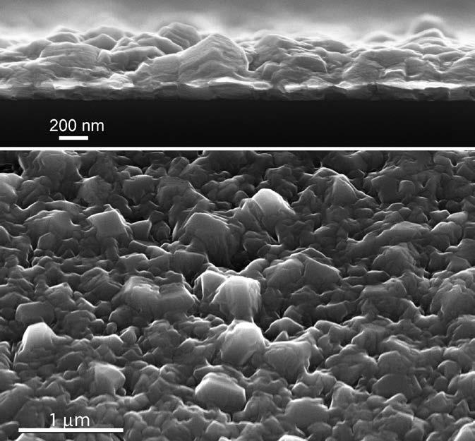
13 Preliminary Nb coatings by HIPIMS Grains as well as defects in substrate are reproduced in the coatings this points to the importance to care (worry!) about the substrate HIPIMS-Nb on chem. polished Cu chemically polished Cu substrate optical micrograph by Anne-Marie Valente-Feliciano, JLab SEM from C. Benvenuti, et al., Physica C: Superconductivity 351 (2001) 421. Observation: Adhesion on aluminum (incl. its oxide) is superior consider aluminum substrates and cavities!
14 Our First T c and RRR Measurements of Nb Nb on Al on Si Test currents A T c = 8.35 K RRR = 4.36, seems disappointingly low, but: measurement includes Al underlayer residual gas contamination expected in hindsight: this sample had a very rough sputtered Al underlayer 14


15 Niobium Films on Aluminum-Silicon Substrates Nb on Al on Si Al on Si 15
16 Great Effect of Temperature indicates: Ion Assistance is still insufficient XRD of Nb on Al on Si At RT: small crystallites At 200 C: gradually greater grains, stress relaxation At 400 C: major change to larger, aligned crystals These films were grown without any bias! future work. 16

17 One more piece of evidence for the importance of the substrate HIPIMS film of Nb on (amorphous!) glass nanocrystalline film 17


18 Custom Movable, Cylindrical Magnetrons for 1.3 GHz Cavities


19 Cylindrical Magnetron - Cavity as Anode sheath plasma ion trajectory possible collision cavity magnetron


20 Dual Magnetron: Most effective for a Biasing Approach: Affecting Ion Energies and Trajectories nearly perpendicular incidence! sheath plasma cavity V bias ion trajectory possible collision magnetron 1 magnetron 2


21 A Dedicated Nb-HIPIMS Berkeley with initial LDRD and later DOE-HEP FY10 funding: chamber for 1.3 GHz SRF cavities base pressure in the low 10-8 range residual gas analyzer 2 small cylindrical, movable magnetrons decoupled substrate heating and biasing pyrometer C 2 SIPP pulsers for dual-hipims and bias

22 A state-of-the-art HIPIMS system for 1.3 GHz, Offering optional dual-hipims and two-material HIPIMS turbo pump gauges cryo pump substrate heater linear motion linear motion movable magnetrons, each with cylindrical Nb target IR temp. sensor magnetron pump
 Dominated by niobium emission Outlook: besides the single and dual magnetron modes, we should extend our goals to other materials Relatively straight forward to include NbN and")
23 HIPIMS Coatings Technology for SRF Cavities dual cylindrical magnetron in at relatively low power sputtering mode Dominated by argon emission dual cylindrical magnetron in high power mode (above runaway threshold) Dominated by niobium emission Outlook: besides the single and dual magnetron modes, we should extend our goals to other materials Relatively straight forward to include NbN and Nb/NbN multilayers One could use two different materials with two asymmetrically operating magnetrons to produce Nb 3 Sn, NbTi alloys, Mg 2 B, and multilayer structures
 Nb has a relatively low")
24 Summary / Conclusions there is a compelling story for thin Nb-film SRF cavities many issues need to be solved, including substrate preparation and coatings technology cathodic arc and HIPIMS are distinct technologies, each delivering an energetic condensation approach HIPIMS has the advantage of not generating macroparticles (assuming that arcing is prevented) Nb has a relatively low self-sputtering yield gasless self-sputtering in vacuum could not be demonstrated low pressure operation works well with optimized pulse frequency. a dedicated HIPIMS system with two cylindrical magnetrons is completed and waiting to be used. Material systems beyond Nb could and should be investigated.