1
|
|
|
- Lynette Henry
- 5 years ago
- Views:
Transcription

 ~1950 1947 Number of transistors per chip doubles every 1.")
1 Analog Chip CAD design tools Process technology Physical layout with L-Edit Neuromorphic Engineering 2 Lecture 3 Cadence Virtuoso Composer XL Schematic editor Cadence Virtuoso Layout XL Layout editor Mentor mmdrc Design rule checker Design Extract Netlist extractor Verification Analog Design Environment Spectre Circuit simulator Mentor mmlvs Layout vs. Schematic Mask layout (GDS finally) L-Edit Outline 1. History and economics of silicon fabrication 2. Fabrication process requirements Your exercise: layout of a composable follower-integrator delay line cell. Bardeen and Brattain Moore s law (or observation) ~ Number of transistors per chip doubles every 1.5 to 2 years Cost/bit drops 29%/year True for last 45 years! 0.25u nm 1

2 ~2000 A finished wafer Historical timeline of fabrication technology development 1930 Lilienfield patents on field-effect transistors Ohl Silicon PN junction Bell labs, Bardeen Brattain make point contact bipolar Phillbrick tube opamp bipolar u 10u 1u 0.25u 90nm 22nm Fairchild founded Accutron watch Kilby/TI integrated circuit, Noyce/Fairchild planar process 63 Widlar/National ua701 opamp Intel founded ($34B sales 2004) Faggin silicon gate 73 Intel 8008 DEC PDP National LM324 opamp 78 Intel 8086 TSMC fab founded ($6B sales 2003) IBM s CMP planarization enables many metal levels Motorola PowerPC 601 nmos CMOS ITRS Roadmap Cost of chip production At 1000 wafers/month (lots of parts!) ~$600/6 inch 0.25u wafer=~$3.50/cm 2 Add for packaging ~0.25 cents/pin for QFP (about most expensive) Add for testing $200/hour for 256 pin mixed signal tester; about 1 second to move sites (6 inch wafer ~ 180 cm 2, 8 inch ~ 310 cm 2 ) From these numbers you can estimate production price of your chip E.g. 40 pin chip of area 5x5mm^2 with 10 second test: Each chip cost 700k parts/month ITRS roadmap - wikipedia Thanks to Chuck Neugebauer for prices ca Inverter layout N-Select (implant) P-Select (NOT N-select) S G holes D S G electrons D n + p + p + n + n + p + n well p well p --- epi (thin oxide) p + wafer 2

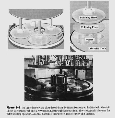
3 CMOS process technology A wafer is photolithograpically processed using a set of masks A typical process has ~15-55 masks Each mask patterns a layer Fabrication occurs in a series of steps: What steps are used in a fabrication process? Pattern Photolithography exposes photoresist to remove it selectively Deposit Use chemical vapor deposition (CVD) or sputtering to coat wafer with layer of stuff Implant Shoots ions into silicon with controlled energy Diffuse Heats wafer to diffuse implants Etch Uses plasmas or wet etches to remove silicon or oxide Polish CMP (Chemical Mechanical Polishing) uses wet slurry and rotating wheels to smooth surface Photolithography a) Wafer preparation b) A photoresist is spun onto the wafer c) The mask is aligned with a stepper d) It is exposed e) The photoresist is chemically developed. Where the resist has been exposed, it is washed away (this is a positive resist) f) The remaining resist blocks an implant or etch g) The resist is removed Wafer prep - Gettering Gathers impurities like Au, Na away from surface by diffusion. Scratched back of wafer along with oxygen interstitials act as nucleation sites. Creates denuded zone at surface. 3
4 Silicon nitride blocks Si oxidation N-Select Si 3 N 4 can be deposited and patterned by photolithography It can be very selectively etched without etching silicon After patterning, it efficiently blocks oxidation of silicon (aka Diff) LOCOS (Local Oxidation of Silicon) (Shallow Trench Isolation) Harder than LOCOS but now used for deep submicron processes Used extensively in the past and still used for many processes 4

5 FOX N-Select P-well=! Ion implantation for doping Simulated ion tracks Doping profiles; note that implants can have retrograde doping, unlike diffusions 5
6 N-select!N-select (P-select) Gate oxide and poly 6

7 N-Select Gate oxide is tricky Nowadays is about 10 atomic layers thick Dangling bonds create havoc by allowing charge to stick Plummer, Deal, Griffen Bravman 7
8 LDD (Lightly Doped Drain) is used in sub-micron processes to reduce the electric field at transistor drains It reduces damage caused by hot electrons It is necessary because power supply voltage has not dropped as quickly as process dimensions 8
9 N-Select P-Select=!N-Select P-Select (NOT N-select) N-select!N-select 9

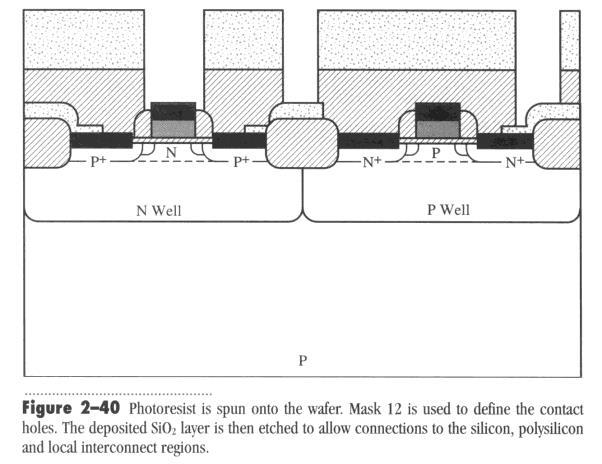
10 N-Select contacts can be separate or butted contacts n + p + p + n + n + p + n well p well p --- epi Butted contacts form uncontrolled lateral pn junctions that must be shorted by metal! Common beginner mistake. These local interconnects are also called Silicidation. They reduce resistance. Called Salicide for and cide for. 10

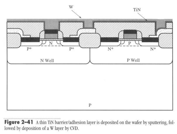
11 CMP N-Select W=tungsten 11


12 Ti/N/W prevents wormholes where Al makes spikes into Si N-Select Schematic-Driven Layout exercise Delay line cell 12
13 Credits for illustrations Plummer, Deal, Griffin Silicon VLSI A. Bergemont in Liu, Indiveri, Kramer, Delbruck, Douglas, Analog VLSI van Zant, Microchip Fabrication 13