Hot wire CVD deposition of nanocrystalline silicon solar cells on rough substrates
|
|
|
- Laureen Potter
- 5 years ago
- Views:
Transcription
00093-5 DOI: doi: 10.1016/j.tsf.2009.01.078 Reference: TSF 25563 To appear in: Thin Solid Films Please cite this article as: Hongbo Li, Karine H.M. van der Werf, Jatin K.")
1 Accepted Manuscript Hot wire CVD deposition of nanocrystalline silicon solar cells on rough substrates Hongbo Li, Karine H.M. van der Werf, Jatin K. Rath, Ruud E.I. Schropp PII: S (09) DOI: doi: /j.tsf Reference: TSF To appear in: Thin Solid Films Please cite this article as: Hongbo Li, Karine H.M. van der Werf, Jatin K. Rath, Ruud E.I. Schropp, Hot wire CVD deposition of nanocrystalline silicon solar cells on rough substrates, Thin Solid Films (2009), doi: /j.tsf This is a PDF file of an unedited manuscript that has been accepted for publication. As a service to our customers we are providing this early version of the manuscript. The manuscript will undergo copyediting, typesetting, and review of the resulting proof before it is published in its final form. Please note that during the production process errors may be discovered which could affect the content, and all legal disclaimers that apply to the journal pertain.
2 Hot wire CVD deposition of nanocrystalline silicon solar cells on rough substrates Hongbo Li*, Karine H. M. van der Werf, Jatin K. Rath, Ruud E. I. Schropp Utrecht University, Faculty of Science, Debye Institute for Nanomaterials Science, P.O. Box 80,000, 3508 TA Utrecht, The Netherland. * Corresponding author. address: h.li@uu.nl Abstract In silicon thin film solar cell technology, frequently rough or textured substrates are used to scatter the light and enhance its absorption. The important issue of the influence of substrate roughness on silicon nanocrystal growth has been investigated through a series of nc-si:h single junction p-i-n solar cells containing i-layers deposited with Hot-wire CVD. It is shown that silicon grown on the surface of an unoptimized rough substrate contains structural defects, which deteriorate solar cell performance. By introducing parameter v, voids/substrate area ratio, we could define a criterion for the morphology of light trapping substrates for thin film silicon solar cells: a preferred substrate should have a v value of less than around , correlated to a substrate surface rms value of lower than around 56 nm. Our Ag/ZnO substrate with rms roughness less than this value typically do not contain microvalleys with opening angles smaller than ~ 110 degree, resulting in solar cells with improved output performance. We suggest a voids-formation model based on selective etching of strained Si-Si atoms due to the collision of growing silicon film surface near the valleys of the substrate. 1
3 Keywords Nanocrystalline silicon, solar cell, rough substrate, hot wire chemical vapour deposition 1. Introduction Thin film solar cells containing hydrogenated nano-crystalline silicon (nc-si:h) absorber layers are being intensively studied [1]. To further increase the energy conversion efficiency while maintaining low production costs, considerable efforts are put in studying and optimizing the light enhancement components such as a rough substrate, in order to sufficiently absorb the incident sun light. Under certain deposition conditions, the structure of the deposited layer generally depends on the substrate used and on the initial stage of the silicon growth. Apart from the influence of the physical/chemical properties of the specific substrate materials such as lattice spacing, atomic bonding properties etc., it is found that substrate roughness can also influence the layer structure, leading to cracks near the micro-valleys of the substrate surface [2,3,4]. While such cracks, due to their very small volume density, typically cannot be observed by bulk material characterization methods such as x-ray diffraction (XRD) or Raman spectroscopy, their influence on device quality can be quite dramatic [2]. A connection between device output performance and the appearance of the microcracks has long been proposed, but an experimental correlation of the presence of cracks with the solar cell J-V characteristics is only proposed very recently [5, 6]. Understanding the origin of the formation of such cracks is of fundamental importance to control the deposition process that would further improve the device performance. In this paper we present our investigation of silicon materials and devices grown on rough Ag/ZnO substrate, and report a correlation of the appearance of observed voids in the nc-si:h layers with the shape of substrate microvalleys, and propose a criterion for the morphology of light trapping substrates for thin film nc-si:h solar cells. 2
4 2. Experimental Details The solar cells discussed in this contribution have a structure of Corning 1737 glass/rough Ag/ZnO/phosphorous doped nc-si:h n-layer/ nc-si:h i-layer/ boron doped nc-si:h p-layer /ITO/Au grid. Except for the surface roughness of the Ag/ZnO coated substrates and a few modifications to the n-layer, the deposition conditions of all other layers (including the silicon layers, ITO and metal grids) are identical. The intrinsic nc-si:h layers were deposited by hotwire CVD and the doped layers by RF PECVD at MHz. ITO, Ag and ZnO layers were made by RF magnetron sputtering. Detailed deposition conditions for these layers have been published previously [2,7]. The roughness of the silver layers was tuned by varying the substrate temperature during Ag sputtering. The substrate surface roughness was characterized with root mean square value (rms) and lateral feature size (L) determined from atomic force microscope (AFM) images. Raman scattering spectroscopy and cross-sectional transmission electron microscopy (XTEM) were used to study the structure of the silicon layers. The XTEM specimens were prepared in an identical process. Solar cell/glass sandwiches were prepared with silicon layers glued facing to each other; they were first cut into thin slices in a direction perpendicular to the substrate surface; then polished to slices of around 20 µm thick, and were further thinned by an ion mill. A FEI Technai 20 electron microscope was used for the XTEM investigation. The solar cells were characterized by current density-voltage (J-V) measurement under dark and AM1.5 illumination at 25 (± 0.5) ºC. 3. Results By varying the Ag deposition conditions, the morphology of the Ag layers can be varied over a wide range. Fig. 1 summarizes the surface properties of the Ag substrates (coated with a 3
5 thin ZnO layer) used for the solar cell deposition. Data points shown in this figure are grouped according to Si deposition runs. Each deposition contains a group of two substrates with different surface roughness. By studying the difference between samples in each group, we can eliminate any run to run difference of Si deposition. The rms value of Ag surface varies from ~10 nm to around ~130 nm, with an average lateral feature size ranging from 0.5 µm to ~ 3 µm (Fig. 1). For the solar cell series deposited on such substrates under exactly the same conditions, the AM1.5 open circuit voltage (V oc ) shows a consistent trend with the rms values, as well as the diode quality factor (n) and reverse saturation current density (J 0 ) (Fig. 2). The structure of silicon stacks grown on such substrates are studied by Raman scattering spectroscopy and cross-sectional transmission electron microscopy (XTEM). Although the normalized Raman scattering spectra of all the samples completely overlap with each other (not shown), the layer structure appeared to be significantly influenced by the roughness of the Ag substrate. In silicon layers deposited on a nearly smooth substrate (rms ~ 4 nm) no cracks are observed (Fig. 3a). When increasing the substrate temperature during sputtering, the substrate rms roughness increases, and stripe-like voids (cracks) start to appear within the micovalleys of the substrate. If we define δ as the angle between adjacent ZnO facets, the appearance of these cracks seems to correlate with the degree of such angle: the smaller the angle is, the wider the cracks are and the more frequently they can be observed in the TEM images. This opening angle crack width dependence is summarized in Fig. 4a, in which the error bar is taken as ± 15 nm for the width measurement and ± 10 degrees for the angle measurement. In valleys with an opening angle larger than a certain value, no voids are formed. This angular threshold has been found to be around 110 o. 4
6 4. Discussion The correlation between the substrate surface roughness and nc-si:h J-V characteristics has been intensively studied recently. It has become more and more clear that the formation of micro-voids or cracks in the bulk silicon layer is one of the most important reasons for the deterioration of the output performance of nc-si:h solar cell deposited on a rough substrate. Under illumination, such performance deterioration is typically reflected by a reduced open circuit voltage (V oc ) [3-6], and sometimes also by a decrease in fill factor (FF) [8]. Due to the absence of photon injection, the solar cell dark J-V characteristics (n and J 0 ) give clearer indication on the electrical influence of such defects. For the samples shown in Fig. 2, except for samples in Group 4 where the difference between their substrate roughness is smaller than the rms error bar, the samples show an increase in n and J 0 values (decrease in V oc ) with increasing substrate rms roughness. The increase of diode quality factor n indicates an enhanced carrier recombination in the bulk of the i-layer. As suggested in references [5, 6], the amount of decrease in solar cell dark J-V performance may be correlated with the density of voids (cracks) in the i-layer, such as that shown in Fig. 3c and Fig. 3d. The rougher the substrate is, the higher the density of these voids might be, and therefore the higher the solar cell J 0 and n values are. If we assume that the mechanism of J-V deterioration or, in simpler words, the appearance of voids is the same for samples made on substrate with various roughness (various rms values), we might be able to correlate J 0 and n values with the density of such voids. A possible description of void density is (1/L) 2, where L is the average lateral feature size of the substrate surface estimated from the substrate AFM images. Fig. 5a and Fig. 5b show the dependence of J 0 and n on the value of (1/L) 2. Surprisingly, in these 5
7 figures we do not observe decreases of J 0 and n with the decrease of (1/L) 2. Instead, they clearly increase. This suggests that the assumptions used above are not valid. Namely, either the void density is not correlated with (1/L) 2 or the appearance of such voids are not the same for samples made on substrates with different roughness. When we look at the AFM images (not shown) of these substrates, we could see that the substrate roughness generally increases with increasing L (Fig. 1), which suggests that the Ag poly-crystalline grains grow larger in both lateral and vertical directions. This type of Ag growth most possibly results in different appearance of the microvalley formed between Ag poly-crystals. From the XTEM images of substrates with different rms values (such as shown in Fig. 3a-d), we can indeed see large differences in the appearance of substrate surface morphology. From Fig. 3a to 3d, the estimated opening angle of the microvalleys shown in these images are ~180, ~120, ~89 and ~30, correlated to substrate rms roughness values of ~ 4nm, ~66nm, ~ 96 nm and ~133 nm respectively. Starting from the sample shown in Fig. 3c, stripe-like voids can often be observed in the XTEM images, the density of which increases with increasing substrate surface rms roughness, so does the width of the voids estimated from the XTEM images. By introducing a parameter v, voids/substrate area ratio, defined as v = mw 2 /l 2, where m is the number of stripe-like voids observed in the XTEM images, w the estimated average void width, and l the measured substrate length as appeared on the XTEM images, we obtain a correlation between v and substrate surface rms roughness, as shown in Fig. 4b. The parameter v contains not only the areal density of the voids but also the average size of the voids observed on each substrate, therefore better characterize the substrate roughness contribution on solar cell V oc and dark J-V properties. From Fig. 4b, one can see that to minimize the 6
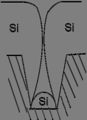
8 deterioration influence of stripe-like voids introduced by substrate roughness, a v value of less than around is needed, correlated to a substrate surface rms value of lower than around 56 nm. Our Ag/ZnO substrate with rms roughness less than this value typically do not contain many valleys with opening angles smaller than 110 degree. From the study on the XTEM images, the appearance of these structural defects clearly connects with the shape of microvalleys formed on the substrate local surface. For Ag layers sputtered at a very high substrate temperature, Ag (poly-) crystals with acute angles formed between the local crystal surfaces and the substrate plane are often observed in the EM images. When two or more of such Ag crystals are adjacent to each other, sharp valleys are formed between them, accompanied by very small opening angles. Silicon grown in these valleys is typically accompanied by large voids located in the middle of the valleys, in which no silicon atoms exist. An image showing this phenomenon is given in Fig. 3d, where the width of the void is estimated to be around 120 nm. (Note that for the sample examined in this image, no ZnO layer is used). Voids with this size may be large enough to short-circuit the complete device, if they extend through the entire i-layer [2]. One of the most possible reasons for the formation of large voids (cracks) is the limited trench coverage ability of silicon growth. Si deposited on the upper surface of the valley may have higher growth rate than on the inner walls. As illustrated in Fig. 6, during Si deposition the thickening films developing around the upper surface of the valley can meet each other before the valley is filled, leaving a large void in the middle of the valley. A similar explanation was used by Sakai et al. for the voids observed in a-si:h layers [9]. 7
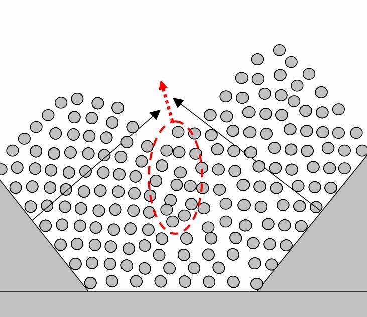
9 One important feature of the voids observed in this set of samples is that once they are formed, they tend to develop along the growth direction and extend further into the bulk of the i- layer, with a trend of decreasing in width as measured from the XTEM images (Fig. 3c and d). Most voids are found to continuously develop up to the top surface of the p-layer. It is obvious that this type of voids should particularly be avoided in a solar cell device. In Fig. 7 we show another possible explanation for the formation of such voids. This is based on the diagrams shown in Fig. 4a. Assuming that Si develops layer by layer on top of the surface of the valley, the local films will grow freely until the layer growth fronts from different plates meet. As soon as they meet, there will be stress created in the silicon network. Due to the high density of atomic hydrogen present during the CVD process, the strained Si-Si bonds may be etched away, resulting in regions with a low density of silicon atoms - a void is therefore formed in that region, (the solid arrows shown in Fig. 7 indicate the layer growth direction; the region encircled with a dashed line: strained atoms that can be easily etched away by H). As long as the layer continues to grow in the same direction, stresses are constantly formed near the corner of the layer growth front. Therefore, the voids will continue to develop along the layer growth direction. By controlling Ag deposition conditions, a surface containing microwells or valleys with low aspect ratio and wide opening angles is obtained. It is observed in TEM images of silicon films on these surfaces, that the presence of voids is reduced or completely eliminated, as that shown in Fig. 3b. We note that the angular threshold (110 º) as marked in the Fig. 4a can be related to the material growth technique and conditions. For the deposition involving plasma CVD, the 8
10 influence of energetic ions on the growth of silicon layer may result in different strain condition between silicon atoms. A slightly different threshold angle might be observed. 5. Conclusions We have presented the correlation between the appearance of the micro-cracks and the substrate surface morphology, and the angular dependence of the width of the nanosized-cracks. Such cracks are the main cause for the deterioration of the single junction nc-si:h n-i-p diode quality when deposited on a rough substrate. By introducing parameter v, voids/substrate area ratio, we could define a criterion for the morphology of light trapping substrates for thin film silicon solar cells, where the nc-si:h layers are deposited directly on the rough surface: a preferred substrate should have a v value of less than around , correlated to a substrate surface rms value of lower than around 56 nm. Our Ag/ZnO substrate with rms roughness less than this value typically do not contain microvalleys with opening angles smaller than ~ 110 degree, resulting in solar cells with improved output performance. We suggest a voids-forming model based on selective etching of strained Si-Si atoms due to the collision of growing silicon film surface near the valleys of the substrate. Further study will be focused on the formation process of such voids in the silicon layers. Acknowledgements The authors thank Ronald Franken and Hans Meeldijk for the sample preparation and part of the TEM images. The research was financed by the Netherlands Agency for Energy and the Environment (SenterNovem) of the Dutch Ministry of Economic Affairs. 9
11 References 1. A.V. Shah, J. Meier, E. Vallat-Sauvain, N. Wyrsch, U. Kroll, C. Droz, U. Graf, Solar Energy Materials & Solar Cells 78 (2003) H. Li, R.H. Franken, R.L Stolk, J.K. Rath, R.E.I. Schropp, Solid State Phenomena (2008) Y. Nasuno, M. Kondo and A. Matsuda, Jpn. J. Appl. Phys. 40 (2001) L J. Bailat, E. Vallat-Sauvain, L. Feitknecht, C. Droz, and A. Shah, J. Appl. Phys. 93 (2003) M. Python, E.Vallat-Sauvain, J.Bailat, D. Dominé, L. Fesquet, A. Shah, C. Ballif, J.Non- Crys. Solids 354 (2008) Hongbo Li, Ronald H. Franken, Jatin K. Rath, Ruud E.I. Schropp, submitted to Sol. Energ. Mat. Sol. C. 7. R.H. Franken, R.L. Stolk, H. Li, C.H.M. van der Werf, J.K. Rath, R.E.I. Schropp, J. Appl. Phys. 102, (2007) Luc Feitknecht, Jerôme Steinhauser, Romain Schlüchter, Sylvie Faÿ, Didier Dominé, Evelyne Vallat-Sauvin, Fanny Meillaud, Christophe Ballif & Arvind Shah, Tech. Digest of PVSEC-15, Shanghai, Oct H. Sakai, T. Yoshida, T. Hama and Y. Ichikawa, Jpn. J. Appl. Phys. 29 (1990)
12 List of table and figure captions Fig. 1 Surface rms roughness of the Ag/ZnO layers used for this study. Samples are grouped according to the Si deposition runs. Lines are a guide to the eye, same to all other figures. Fig. 2 Dependence of solar cell J-V characteristics (V oc, J 0 and n) on substrate surface rms roughness. Fig. 3 XTEM images of nc-si:h n-i-p cells deposited under identical conditions but on Ag/ZnO coated Corning glass substrates (except for Fig.3d, where only Ag is present) with various roughness. From a) to d), the rms values for each substrates are ~ 4 nm, ~ 66 nm, ~ 96 nm and ~133 nm respectively. The angle and width values marked in the figures are (89º, 17nm) for Fig. 3c and (30º, 94 nm) and (110º, 2 nm) for Fig. 3d. The scale bar shown in Fig. 3d is 200nm. Fig. 4 a) Correlation between the opening angle of the Ag/ZnO surface texture and the diameter of the microvoids (white stripes) determined from the TEM images of the n-i-p samples. b) Correlation of the area ratio of voids and substrate, v, and substrate surface rms roughness. Fig. 5 Correlation of solar cell dark J-V characteristics (J 0 and n) on (1/L) 2, where L is the lateral feature size of the substrate surface. Fig. 6 Formation of large voids due to limited trench coverage ability of nc-si:h growth. Fig. 7 Diagram of a possible mechanism for the formation of cracks, where H etching on strained Si-Si bond is depicted. 11
13 Fig. 1 lateral feature size (nm) rms (nm) group1 group2 group3 group4 12
14 Fig. 2 Voc (V) Dark Current Density J 0 (ma/cm 2 ) a) Group 1 Group 2 Group 3 Group 4 Substrates rms roughness (nm) 1E-6 Group 1 Group 2 Group 3 Group 4 1E-7 b) 1E Substrates rms roughness (nm) 13
15 Diode Quality Factor n Group 1 Group 2 Group 3 Group Substrates rms roughness (nm) c) 14


16 Fig. 3 a c ZnO/Ag nc-si:h i-layer ITO ITO b nc-si:h i-layer nc-si:h i-layer nc-si:h i-layer Ag Ag/ZnO d ZnO/Ag Glass 15
17 Fig. 4a diameter of the strip-like voids (nm) Fig. 4b estimated voids/substrate area ratio Si no stripes observed opening angles of Ag/ZnO surface texture (degree) 10-3 b) no stripes-like voids observed rms (nm) 16
18 Fig. 5 n J 0 ma/cm 2 1E-6 1E-7 1E /L 2 (μm -2 ) group1 group2 group3 group4 group1 group2 group3 group /L 2 (μm -2 ) 17

19 Fig. 6 18
20 Fig. 7 19