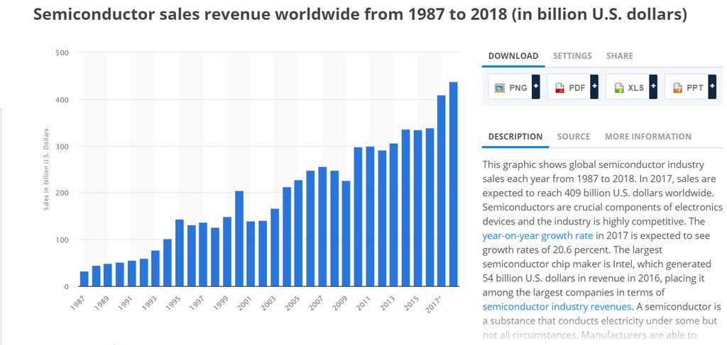
IC Fabrication Technology Part III Devices in Semiconductor Processes
|
|
|
- Abigail Willis
- 5 years ago
- Views:
Transcription
1 EE 330 Lecture 10 IC Fabrication Technology Part III Metalization and Interconnects Parasitic Capacitances Back-end Processes Devices in Semiconductor Processes Resistors Diodes

2
3
4

5
6 Review from Last Lecture IC Fabrication Technology Crystal Preparation Masking Photolithographic Process Deposition Etching Diffusion Ion Implantation Oxidation Epitaxy Polysilicon Planarization Contacts, Interconnect and Metalization
7 Review from Last Lecture Contacts A A B B Acceptable Contact Unacceptable Contact Vulnerable to pin holes (usually all contacts are same size)
8 Review from Last Lecture Contacts B B Acceptable Contact
9 Contacts 2λ 2λ 1.5λ 1.5λ 2λ Dog Bone Contact Design Rule Violation
10 Contacts Common Circuit Connection Standard Interconnection Buried Contact Can save area but not allowed in many processes
11 Metalization Aluminum widely used for interconnect Copper often replacing aluminum in recent processes Must not exceed maximum current density around 1ma/u for aluminum and copper Ohmic Drop must be managed Parasitic Capacitances must be managed Interconnects from high to low level metals require connections to each level of metal Stacked vias permissible in some processes
12 Metalization Aluminum Aluminum is usually deposited uniformly over entire surface and etched to remove unwanted aluminum Mask is used to define area in photoresist where aluminum is to be removed Copper Plasma etches not effective at removing copper because of absence of volatile copper compounds Barrier metal layers needed to isolate silicon from migration of copper atoms Damascene or Dual-Damascene processes used to pattern copper
13 Patterning of Aluminum Contact Opening from Mask Photoresist
14 Patterning of Aluminum Contact Opening after SiO 2 etch Photoresist
15 Patterning of Aluminum Contact Opening after SiO 2 etch Photoresist
16 Patterning of Aluminum Metal Applied to Entire Surface
17 Patterning of Aluminum Photoresist Patterned with Metal Mask
18 Patterning of Aluminum Aluminum After Metal Etch (photoresist still showing)
19 Copper Interconnects Limitations of Aluminum Interconnects Electromigration Conductivity not real high Relevant Key Properties of Copper Reduced electromigration problems at given current level Better conductivity Challenges of Copper Interconnects Absence of volatile copper compounds (does not etch) Copper diffuses into surrounding materials (barrier metal required)

20 Source: Sept 13, 2017
21
22
23 Copper Interconnects Practical methods of realizing copper interconnects took many years to develop Copper interconnects widely used in some processes today
24 Damascene Process Patterning of Copper Contact Opening after SiO 2 etch Photoresist
25 Damascene Process Patterning of Copper Tungsten (W) CMP Target W has excellent conformality when formed from WF6

26 Chemical-Mechanical Planarization (CMP) Polishing Pad and Wafer Rotate in non-concentric pattern to thin, polish, and planarize surface Abrasive/Chemical polishing Depth and planarity are critical Acknowledgement:
27 Patterning of Copper Damascene Process After first CMP Step CMP Target W-plug
28 Damascene Process Patterning of Copper After first CMP Step Oxidation
29 Damascene Process Patterning of Copper Photoresist Patterned with Metal Mask Defines Trench
30 Patterning of Copper Damascene Process Shallow Trench after Etch W-plug
31 Damascene Process Patterning of Copper Barrier Metal (Barrier metal added before copper to contain the copper atoms)
32 Damascene Process Patterning of Copper W-plug Copper Deposition
33 Patterning of Copper Damascene Process W-plug CMP Target Copper Deposition Copper is deposited or electroplated (Barrier Metal Used for Electroplating Seed)
34 Patterning of Copper Damascene Process After Second CMP Step W-plug Copper CMP Target
35 Dual-Damascene Process Patterning of Copper Shallow Trench Defined in PR with Metal Mask Photoresist
36 Dual-Damascene Process Patterning of Copper Shallow Trench After Etch Photoresist
37 Dual-Damascene Process Patterning of Copper Via Defined in PR with Via Mask Photoresist
38 Dual-Damascene Process Patterning of Copper Via Etch Defines Contact Region Photoresist (Barrier Metal added before copper but not shown)
39 Dual-Damascene Process Patterning of Copper Copper Deposited on Surface Copper is deposited or electroplated (Barrier Metal Used for Electroplating Seed)
40 Dual-Damascene Process Patterning of Copper Copper Deposited on Surface CMP Target
41 Dual-Damascene Process Patterning of Copper Copper Via Copper Interconnect CMP Target
42 Patterning of Copper Both Damascene Processes Realize Same Structure Damascene Process Two Dielectric Deposition Steps Two CMP Steps Two Metal Deposition Steps Two Dielectric Etches W-Plug Dual-Damascene Process One Dielectric Deposition Steps One CMP Steps One Metal Deposition Steps Two Dielectric Etches Via formed with metal step
43 Multiple Level Interconnects 3-rd level metal connection to n-active without stacked vias
44 Multiple Level Interconnects 3-rd level metal connection to n-active with stacked vias
45 Interconnect Layers May Vary in Thickness or Be Mostly Uniform Metalization 12.5μ
46 Interconnects Metal is preferred interconnect Because conductivity is high Parasitic capacitances and resistances of concern in all interconnects Polysilicon used for short interconnects Silicided to reduce resistance Unsilicided when used as resistors Diffusion used for short interconnects Parasitic capacitances are high
47 Interconnects Metal is preferred interconnect Because conductivity is high Parasitic capacitances and resistances of concern in all interconnects Polysilicon used for short interconnects Silicided to reduce resistance Unsilicided when used as resistors Diffusion used for short interconnects Parasitic capacitances are high
48 Resistance in Interconnects B W A L H A R B
49 Resistance in Interconnects B W D A H L R L A ρ D R B A=HW ρ independent of geometry and characteristic of the process
50 Resistance in Interconnects B W D A H H << W and H << L in most processes Interconnect behaves as a thin film Sheet resistance often used instead of conductivity to characterize film R =ρ/h R=R [L / W] R L L A ρ L W ρ H
51 Resistance in Interconnects W L R=R [L / W] The Number of Squares approach to resistance determination in thin films N S = 21 L / W=21 R=R N S
52 Resistance in Interconnects Fractional Squares Can Be Represented By Their Fraction Corners Contribute about.55 Squares The squares approach is not exact but is good enough for calculating resistance in almost all applications In this example: N S = =13.25 R=R 13.25
53 Example: The layout of a film resistor with electrodes A and B is shown. If the sheet resistance of the film is 40 Ω/, determine the resistance between nodes A and B. 10u A 3u 1u B
54 Solution 10u A 3u 1u B N S = (.55)=22.1 R AB =R N S =40x22.1=884Ω
55 Resistance in Interconnects (can be used to build resistors!) Serpentine often used when large resistance required Polysilicon or diffusion often used for resistor creation Effective at managing the aspect ratio of large resistors May include hundreds or even thousands of squares
56 Resistance in Interconnects (can be used to build resistors!) d 2 2 d 1 Area requirements determined by both minimum width and minimum spacing design rules
57 End of Lecture 10