Lecture 3: Description crystal structures / Defects
|
|
|
- Anabel Cannon
- 5 years ago
- Views:
Transcription

1 Lecture 3: Description crystal structures / Defects Coordination Close packed structures Cubic close packing Hexagonal close packing Metallic structures Ionic structures with interstitial sites Important structure types Defects Point defects Solid solutions Extended defects Dislocations Figures: AJK 1
2 Coordination (1) Ref: Müller p. 5 2
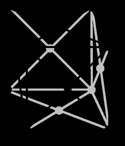
3 Coordination (2) (dodecahedral = 12 faces. The polyhedron shown is actually a snub disphenoid) Ref: Müller p. 5 3

4 Close Packing (1) Many metallic, ionic, covalent and molecular crystal structures can be described using the concept of close packing (cp) The structures are usually arranged to have the maximum density and can be understood by considering the most efficient way of packing equal-sized spheres The most efficient way to pack spheres in two dimensions is shown below Each sphere, e.g. A, is in contact with six others -> six nearest neighbours and the coordination number, CN = 6 (the largest possible for a planar arrangement) (a) a cp layer of equal-sized spheres; (b) a non-cp layer with coordination number 4; Within a cp layer, three close packed directions xx, yy, and zz occur Ref: West p. 19 4

: Third layer at T, layer sequence ABCABC (c, d) alternative positions P and R for a second cp layer Ref: West p. 20 Two cp layers A and B.")
5 Close Packing (2) The most efficient way to pack spheres in three dimensions is to stack cp layers on top of each other There are two simple ways to do this, resulting in hexagonal close packed and cubic close packed structures The most efficient way for two cp layers A and B to be in contact is for each sphere of one layer to rest in a hollow between three spheres in the other layer (P or R) Addition of a third cp layer can also be done in two ways: Hexagonal close packing (hcp): Third layer at S, layer sequence ABABAB Cubic close packing (ccp): Third layer at T, layer sequence ABCABC (c, d) alternative positions P and R for a second cp layer Ref: West p. 20 Two cp layers A and B. The B layer occupies the P positions 5
6 Close Packing (3) The simplest layer stacking sequences hcp and ccp are the most important ones More complex sequences with larger repeat units, e.g. ABCACB or ABAC can occur and some of these give rise to the phenomenon of polytypism. In a 3D cp structure, each sphere is in contact with 12 others 74.05% of the total volume is occupied by spheres (maximum density possible in structures constructed of spheres of only one size) Ref: West p. 21 6


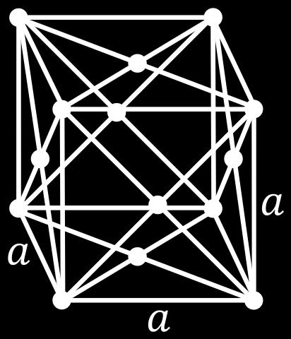
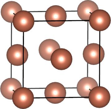
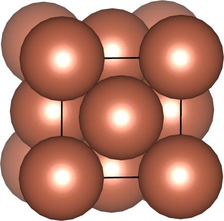
7 ccp = fcc Body diagonal The unit cell of a ccp arrangement is in fact face centered cubic (fcc) A B C A Figure: Wikipedia F (fcc) Cu (fcc metal) Figures: AJK 7

8 hcp hcp structure of Zn metal (space group P6 3 /mmc) The structure is slightly distorted, with 6 neighbors at 2.66 Å and 6 at 2.91 Å A B A B Figure: AJK 8
9 Structures of common metals Most metals crystallise in one of the three arrangements, ccp (fcc) hcp or bcc bcc is not a close packed structure! It is still not well understood why particular metals prefer one structure type to another Calculations reveal that the lattice energies of hcp and ccp metal structures are comparable and, therefore, the structure observed in a particular case probably depends on fine details of the bonding requirements or band structures of the metal Ref: West p. 25 9


![..] = predicted](/docs-images/89/97717324/images/10-5.jpg "structure P I")
10 Periodic table of crystal structures Legend:.. /.. = mixed structure [...] = predicted structure P I (bcc) F (fcc) Figures: Wikipedia 10
11 Close packing in ionic structures The structures of materials such as NaCl, Al 2 O 3, Na 2 O and ZnO, in which the anion is larger than the cation, are built of cp layers of anions with the cations placed in interstitial sites Many structures are possible in which the variables are the anion stacking sequence, either hcp or ccp, and the number and type of interstitial sites occupied by cations. The cations are, however, often too large for the prescribed interstitial sites and the structure can accommodate them only by expanding the anion array Consequently, the anion arrangement is the same as in cp, but the anions may not be in contact (the term eutactic has been suggested for such structures) Furthermore, the rigid sphere model is an oversimplification of reality since, in ionic structures, it can be difficult to specify ion sizes exactly. Two types of interstitial site, tetrahedral and octahedral, are present in cp structures Ref: West p

12 T +, T, and O sites Ref: West p
13 Examples of interstitial sites It is rare that all the interstitial sites in a cp structure are occupied; often one set is full or partly occupied and the remaining sets are empty Ref: West p


14 Octahedral interstitials in NaCl structure Na Cl Figures: AJK 14
15 Cation sites in an fcc anion array Ref: West p

16 Close packing in covalent structures Some materials such as diamond and silicon carbide, which have very strong, directional, covalent bonds, can also be described as cp structures or eutactic structures Diamond can be regarded as a sphalerite structure as ionic compounds in which half of the C atoms form a ccp array and the other half occupy T + sites The two types are equivalent since there are only carbon atoms! Classification of diamond as a eutactic structure is useful since in diamond all atoms are of the same size and it is unrealistic to distinguish between packing atoms and interstitial atoms F (fcc) Ref: West p. 31 Diamond structure, T + sites highlighted Figure: AJK 16
 sites occupied (anion and cation sites are interchangeable) Na 2 O (antifluorite), T + and T - sites occupied F (fcc)")
17 Cubic structure types with fcc anion array Figures: AJK Na Cl Zn S Na O NaCl (rocksalt) O sites occupied ZnS (zincblende), T + (or T - ) sites occupied (anion and cation sites are interchangeable) Na 2 O (antifluorite), T + and T - sites occupied F (fcc) 17
18 NaCl/ZnS -type structures Ref: West p

19 Fluorite/antifluorite structures Figures: AJK F Na Ca O Ref: West p. 41 CaF 2 (fluorite) Na 2 O (antifluorite) 19


20 CsCl structure Primitive cubic, not body centered cubic since there are different ions at corner and body center positions! The anion and cation sites are interchangeable Figures: AJK Ref: West p

, T +")
: O sites")

21 Hexagonal structure types with hcp anion array Figures: AJK Ni Zn As O ZnO (wurtzite - ZnS), T + (or T - ) sites occupied NiAs (NiAs): O sites occupied. Coordination: Ni octahedral (6); As trigonal prism (6) 21
22 Wurtzite/NiAs type structures Ref: West p
23 Interatomic distances in some simple structures Ref: West p

24 Defects In a perfect crystal, all the atoms are at rest on their correct lattice positions Such a perfect crystal can be obtained, hypothetically (or computationally), only at absolute zero; at all real temperatures, crystals are imperfect Atoms vibrate, which may be regarded as a form of defect, but also a number of atoms are inevitably misplaced In some crystals, the number of defects may be very small, <<1%, as in, e.g., highpurity silicon, diamond, or quartz In highly defective crystals, the question often arises as to whether the defects themselves should be regarded as forming a fundamental part of the structure rather than as some imperfection in an otherwise ideal structure. Pure diamonds, before and after irradiation and annealing. Clockwise from left bottom: 1) Initial (2 2 mm) 2 4) Irradiated by different doses of 2-MeV electrons 5 6) Irradiated by different doses and annealed at 800 C. Ref: West p. 83 Figure: Wikipedia 24
25 Why do crystals have defects? Crystals are invariably imperfect because the presence of defects up to a certain concentration leads to a reduction of free energy (Figure 2.1) Let s consider the effect on the free energy of a perfect crystal of creating a single defect (e.g. a vacant cation site) This requires a certain amount of energy, ΔH It also causes a considerable increase in entropy, S, because of the large number of positions which this defect can occupy (configurational entropy) At some point, the energy required to create more defects will be larger than any subsequent gain in entropy ΔG = ΔH - TΔS S = k B ln W W = number of possible configurations for one mol of cations! Ref: West p
26 Defect types (1) For a given crystal, curves such as shown in Fig. 2.1 can be drawn for every possible type of defect and the main difference between them is the position of their free energy minimum The defect that predominates is the one which is easiest to form, i.e. with the smallest ΔH and for which the free energy minimum occurs at the highest defect concentration In Table 2.1, the defects which predominate in a variety of inorganic solids are summarized Ref: West p
27 Defect types (2) One classification of defect types: Stoichiometric defects, in which the crystal composition is unchanged on introducing the defects (also called intrinsic defects) Non-stoichiometric defects, which are a consequence of a change in composition (also called extrinsic defects) Another classification based on the size of the defect: point defects involve only one atom or site, e.g. vacancies or interstitials, although the atoms surrounding the defect are also somewhat perturbed line defects, i.e. dislocations, are effectively point defects in two dimensions but in the third dimension the defect is very extensive or infinite; in plane defects, whole layers in a crystal structure can be defective Sometimes the name extended defects is used to include all those which are not point defects Ref: West p
28 Schottky defect In ionic solids such as halides or oxides, the Schottky defect, a stoichiometric defect, is a pair of vacant sites, an anion vacancy and a cation vacancy To compensate for the vacancies, there should be two extra atoms at the surface of the crystal for each Schottky defect The Schottky defect is the principal point defect in the alkali halides Equal numbers of anion and cation vacancies required to preserve local electroneutrality Vacancies tend to associate because they attract each other For NaCl at room temperature, typically one in of the sites is vacant In other terms, 1 mg of NaCl (~10 19 atoms) contains ~10 4 Schottky defects Schottky defects are responsible for the optical and electrical properties of NaCl Ref: West p

29 Frenkel defect An atom displaced off its lattice site into an interstitial site that is normally empty AgCl (with the NaCl crystal structure) has predominantly this defect (interstitial Ag) There is probably some covalent interaction between the interstitial Ag + ion and its four Cl neighbours which acts to stabilise the defect and give Frenkel defects, in preference to Schottky defects, in AgCl Na + with its harder, more cationic character, would not find much comfort in a site which was tetrahedrally surrounded by four other Na+ ions. Frenkel defects therefore do not occur to any significant extent in NaCl Calcium fluoride, CaF 2, has predominantly anion Frenkel defects in which F occupies interstitial sites As with Schottky defects, the vacancy and interstitial are oppositely charged and may attract each other to form a pair Ref: West p
30 Color centers (1) The best known example of a color center is the F-center (Farbzentrum), which is an electron trapped on an anion vacancy (Figure) F-centres can be prepared by heating an alkali halide in vapour of an alkali metal NaCl heated in Na vapour becomes slightly non-stoichiometric due to the uptake of Na to give Na 1+δ Cl (δ << 1), which has a greenish yellow colour The trapped electron provides a classic example of an electron in a box. A series of energy levels are available for the electron within this box and the energy required to transfer from one level to another falls in the visible part of the electromagnetic spectrum Ref: West p
31 Color centers (2) Many other colour centres have been characterised in alkali halide crystals H- and V-center containing the chloride molecule ion Cl 2 are shown in the Figure Other defect centers which have been identified in the alkali halides include: the F -center, which is two electrons trapped on an anion vacancy the FA-center, which is an F-center, one of whose six cationic neighbors is a foreign monovalent cation, e.g. K+ in NaCl the M-center, which is a pair of nearest neighbour F-centres the R-center, which is 3 nearest neighbour F-centres located on a (111) plane ionised or charged cluster centres, such as M +, R + and R Ref: West p
32 Solid solutions In extrinsic defects associated with dopants or impurities, the dopants either occupy interstitial sites or substitute for atoms or ions in the parent lattice As the dopant concentration rises, above 0.1 1%, it is common practice to refer to the materials as solid solutions rather than as doped materials, but these two terminologies are interchangeable A solid solution is basically a crystalline phase that can have variable composition. As with doped crystals, simple solid solutions are one of two types: in substitutional solid solutions, the atom or ion that is being introduced directly replaces an atom or ion of the same charge in the parent structure in interstitial solid solutions, the introduced species occupies a site that is normally empty and no ions or atoms are left out Starting with these two basic types, a considerable variety of more complex solid solution mechanisms may be derived Ref: West p

33 Some extended defects Stacking faults are plane defects that are common in materials with layered structures, especially those that exhibit polytypism For example: Co metal exhibits both polytypism and stacking faults. It occurs in two main polytypes, either ccp (ABC) or hcp (AB). Stacking disorder occurs when the normal stacking sequence is interrupted by the presence of wrong layers, e.g.... ABABABABCABABA Subgrain boundaries and antiphase domains (boundaries) Within the domains, typically Å in size, the structure is relatively perfect, but at the interface between domains there is a structural mismatch Another type of boundary, an antiphase boundary, involves a relative lateral displacement of two parts of the same crystal Ref: West p
34 Dislocations Dislocations are an extremely important class of crystal defect They are responsible for the relative weakness of pure metals and in certain cases (after work-hardening) for just the opposite effect of extra hardness The mechanism of crystal growth from either solution or vapour appears to involve dislocations Reactions of solids often occur at active surface sites where dislocations emerge from the crystal Dislocations are stoichiometric line defects Dislocations can be one of two extreme types, edge or screw dislocations, or can have any degree of intermediate character Ref: West p
35 Edge dislocation A simple edge dislocation is an extra half-plane of atoms, i.e. a plane of atoms that goes only part of the way through a crystal structure To understand the effect of dislocations on the mechanical properties, consider the effect of applying a shearing stress to a crystal that contains an edge dislocation Ref: West p