DEVELOPMENT OF A DEEP TRENCH RIE ETCH FOR CAPACITOR AND ISOLATION TECHNOLOGIES
|
|
|
- Nigel Dickerson
- 5 years ago
- Views:
Transcription
1 DEVELOPMENT OF A DEEP TRENCH RIE ETCH FOR CAPACITOR AND ISOLATION TECHNOLOGIES Joseph W. Wisemari Senior Microelectronic Engineering Student Rochester Institute of Technology ABSTRACT A silicon trench 2um deep was etched in a PlasmaTher m 246 RIE tool using an SF6/C2 chemistry with an oxide mask. The single crystal silicon etch rate was 11A/min, with a high selectivity to oxide. A trench slope approximately 5 degrees was obtained, with no undercut of the oxide mask. INTRODUCTION The development of trenches for capacitors and device isolation is essential to meet the demands for increased circuit densities. Continued shrinking of device sizes may be limited by the size of capacitors and isolation areas. One such application where this is evident is a capacitive structure for DRAM cells. Since there is a minimum charge necessary for reliability concerns, the gate area of the capacitor cannot be reduced into the submicron range [1]. Thus for the two dimensional DRAM, shown in Figure 1, the area of stored charge occupies significant portion of the cell. In order to solve this problem, a trench capacitor can be used to minimize the area occupied on the surface, while still maintaining the necessary charge in the device. A trench capacitor is a device that utilizes a third dimension(depth into the silicon), so that it consumes less area on the surface of the wafer and still meets the minimum requirements for stored charge. METAL7 STORAGE GATE TRANSFER GATE IMPLANTS~ LBIT LINE Figure 1: DRAM cell with two dimensional capacitance [2]. To create a trench capacitor, a trench with a relatively high aspect ratio (meaning a large depth etched from a narrow opening) is needed. A Reactive Ion Enhanced(RIE) etch with high selectivity to the oxide mask is needed to form the deep trench etch with vertical sidewalls. The etched trenches will then be filled with a dielectric and polysilicon for the capacitor structure. 171
2 In order for the fill to be successful, the resultant profile should have a sidewall slope around 87 degrees and be slightly rounded at the bottom to reduce stress effects [3]. If the slope is greater than 87 degrees, the filling of the trench will be pinched off, due to corner enhanced oxidation during the oxide growth and the conformal properties of the polysilicon filling the trench. A rounded profile at the bottom of the trench is desired for filling purposes as well, and can be obtained with a brief isotropic etch at the end of the RIE etch [4]. A DRAM cell with a trench capacitor is illustrated in Figure 2, along with the critical concerns of trench formation. Al DATA LINE TO Figure 2: DRAM trench capacitor and critical areas [5]. Common isolation techniques are also obstacles to smaller dimensions. In particular, the LOCOS process can not be made smaller as easily as capacitors, because of the bird s beak. The bird s beak is a phenomenon that comes from lateral oxidation that can narrow device regions when smaller geometries are attempted. This growth laterally is as long as the total oxidation is high, thus not allowing it to be diminished or eliminated without a more complicated process. Trench isolation can go deeper into the substrate in a smaller horizontal dimension and give the same, if not better, isolation. Figure 3 shows the bird s beak effect from LDCDS limiting the active region to about 1.5um. Also shown is the trench isolation does not encroach on the active area and allows for narrower channels. A trench for isolation is formed with the same etch as the capacitors, but the trench is commonly filled with a dielectric only. Bird s Beak Encroachm.nt ~h. I/, Field oxide / ///// II NItnd~.y.r Figure 3: LOCOS isolation versus Trench isolation [6]. 9_1~I~1 To form a deep trench with vertical sidewalls a RIE process is required which removes silicon from the horizontal surfaces while forming polymers on the sidewalls. Gases commonly used in the industry include: HBr, NF3, CF4/2, Cl2, CC14, CC13F, or SF6/CBrF3. Chlorine is the primary etchant because of its slow 172
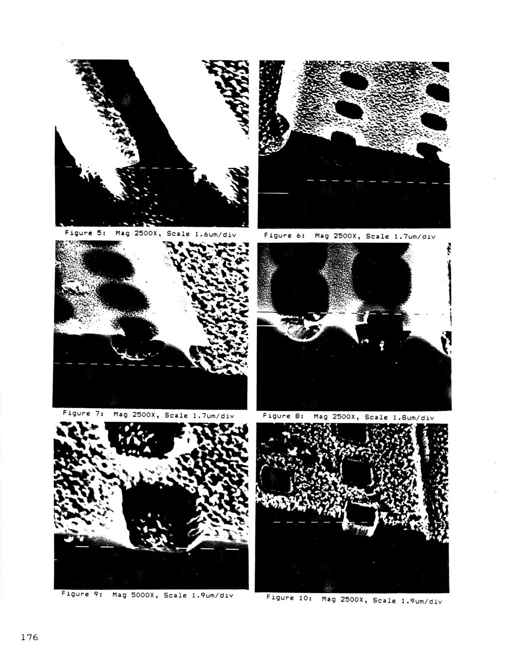
3 reactivity on the sidewalls, thus producing a more anisotropic etch through sidewall passivation. It has been reported in literature that problems with bowing in the trench exists. The phenomenon of bowing can be seen by the rounded edges inside the trench, as shown in Figure 4. One cause for bowing is that at higher pressures there are more molecular interactions in the plasma, so that the higher chance of collision and scattering cause the etching of the sidewalls below the surface. This problem, however, has not been evident in trench openings greater than 2um wide [7]. Figure 4: Trench bowing effect [B]. Since the gases mentioned above are primarily hazardous, they were not available for use in our lab. ~ standard SF6/D2 process for isotropic (same etch rate in all directions) polysilicon etching cannot produce vertical sidewalls. Improving the anisotropy was investigated by reducing pressure and increasing power to encourage more ionic bombardment. This led to the use of C2 to create a situation for sidewall passivation, due to the unsuccessful attempts with modifying the standard isotropic process. The C2 will dissociate in the plasma and some of the C in the plasma will react with the F ions generated from the dissociation of the SP~ in the plasma, this can form CF2 to polymerize the sidewalls of the trench during the etch. EXPERIMENT Twelve 3, <1> silicon wafers were obtained and scribed with DT-1 to DT 15. ~pproximately 6A of thermal oxide was grown on the wafers. They were then coated with 1.2um of KTI-82 positive photoresist. The photoresist was patterned with a test mask containing various sizes of line/space pairs and square openings. ~fter patterning the photoresist, the oxide mask was etched in the RIE tool. For all the etches the substrate cooling was set at its minimum, which kept the temperature between 16-1BC. The process parameters used were CHF3 flow of 6sccm, C2F6 flow of l7lsccm, pressure of 127mT, and power of 35W. ~fter etching the oxide mask, the remaining photoresist was ashed off half of the wafers, ji~ order to examine the effects of extra carbon in the plasma for creating sidewall passivation. Two wafers were then etched with the SF6/D2 chemistry to explore the anisotropy of the etch. Wafer DT-1, which had the patterning resist it was etched for 7 sec with conditions of SF6 flow of 3Osccm, 2 flow of lsccm, pressure of loomt, Power of 3W. Wafer DT-2 was etched for about 24 sec with the following 173
4 process: SF6 flow of lsccm, 2 flow of 3sccm, pressure of 6OmT, power of 25W. Seven wafers saw the addition of various amounts of CO2 to the etch process used for DT-2. Recall that some of these wafers still had the resist layer, thus not only was C2 varied in this experiment, but the presence or absence of resist as well. Table 1 shows the variation in C2 flow for these seven wafers. Finally, wafer DT-15 was etched for 3 minutes with the power increased to 35W, and a CO2 flow of 3sccm. The last 2 wafers were lost. Wafer # Mask C2 flow(sccm) Etch Time(min) DT 4 Oxide 5 1 DT-8 Oxide 1 15 DT-9 Oxide 2 15 DT-1 Oxide 4 1 DT-12 PR + Oxide 5 1 t)t-13 PR + Oxide 2 15 DT-14 PR + Oxide 4 2 Table 1: Experimental Parameters for the SF6 + C2 runs. RESULTS/DISCUSSION The wafers were evaluated with an ~lpha-step Profilometer and a SEM for verification of trench depths and profiles. For the wafers etched with SF6 and 2, there were Si etch rates (vertical) of 1-1.5um/min, with the latter etch rate for wafer DT-2. ~s expected, the etch was almost perfectly isotropic, etching only twice as fast vertically, as horizontally. The etch depths for DT-1 and 2 were 1 and 6um respectively, with the undercutting of the oxide mask being of approximately 5 and 3um. This can be seen in the corresponding SEM micrographs in Figures 5 and 6. The CO2 addition proved to be successful in passivating the sidewall, with the etch rate decreasing significantly with the increased CO2 flow. The results of this experiment are shown in Table 2 below, with the etch rates(er) in 1~/min. Wafer # Vert ER Hor ER Depth Undercut Fig ~ DT DT DT DT DT DT DT Table 2: Data for SF6/C2 experiment Overall, the C2 addition had a dramatic impact on the sidewall slope,, with results that predict a better process. From a graph of the vertical and horizontal etch rates, shown in Figure 11 at the end, it can be seen that the horizontal etch rate approaches zero around a F::C ratio of 2.6::1. This ratio is theoretical, but it predicts a process flow with 13 sccm of SF6 and 3 sccm of CO2. With these flows and the same etch parameters used for the seven 174
5 wafers in the C2 experiment, vertical sidewalls should be obtained. This result was verified by an equation developed to express the anisotropy of the trench. This relationship, as shown on the graph in the appendix, shows that 1~ anisotropy(or a vertical sidewall) would occur around a F:C ratio of 2:1, which is very similar to the results obtained from the etch rates alone. Figures 7, 6, and 9 show the change in the profile as the C2 flow was increased for wafers DT-9, 12 and 14, respectively. The polymer formation on wafer DT-14 is shown in Figure 1. CONCLUSIONS The SF6/C2 chemistry proved to be an effective method for, obtaining a more anisotropic trench profile, when compared to the SF6+2 chemistry. From the etch rates obtained during the C2 experiments, it can be concluded that an optimum process would be: SF6 flow of l3sccm, C2 flow of 3sccm, pressure of 6OmT, power of 25W. This process should be attempted, with a wafer patterned with photoresist on about 6P~ of oxide. The trench obtained, however, may have extreme problems with polymer formations, that cannot be removed. ~ method should be investigated to remove of these polymers, along with possibly trying a CF4/2 chemistry. ACKNOWL EDGMENTS I would like to thank the following people for their contributions to the Deep Trench Etch pro.~ect: Dr. Richard Lane, Prof. Mike Jackson, Mr. Gary Runkle, Mr. Scott Blondell, Mr. Daniel Morvay and Mr. Eric Thompson. REFERENCES [1] S. Wolf, Silicon ProcessinQ for the VLSI Era: Volume 2, Chapter 4, 199. [2] ibid, p [3] ibid, pp [4] ibid, p. 54. [5] ibid, p. 63. [6] ibid, pp. 24, 52. [7] M. Ameen, M. Monfils, Z. Hasan, and D. Gates, Semiconductor International, 126 (Sep 1988). [8] 6. Herb, Advanced Plasma Processes, NATO Advanced Study Institute, Live Satellite Broadcast, Apr 22, 1991, p
6 3
7 Etch Rates vs. F::C Ratio (Negative Lateral E.R. means no undercut) ER-Vertical ER-Lateral LU F::C Ratio I Anisotropy vs. F::C Ratio (For anisotropy = 1%, sidewalls = 9 ) 2 > LU LU >. ~ ~ 1 Anisotropy ~ I- U, C F::C Ratio Figure 11: Graphs of etch rate results 177