An SOI Process for Fabrication. of Solar Cells, Transistors and Electrostatic Actuators. Berkeley Sensor and Actuator Center
|
|
|
- Abigayle Fitzgerald
- 5 years ago
- Views:
Transcription
1 An SOI Process for Fabrication of Solar Cells, Transistors and Electrostatic Actuators Colby L Bellew, Seth Hollar and K.S.J. Pister University of California at Berkeley Berkeley Sensor and Actuator Center
2 Target Applications Autonomous Microsystems Distributed sensor networks - SmartDust Microrobots System Components Power sources Circuits Actuators/Sensors

3 Golem Dust
4 Process Goals Integration - Simplify Reduce the number of separate components Simplify assembly Reduce size Solar Power Reduce/eliminate need for stored power Increase life of device High-Aspect Ratio MEMS Devices Wide range of possible sensors and actuators
5 Deputy Dust
6 System Architecture Two chip solution for autonomous MEMS MEMS chip power and actuation High voltage solar cell arrays Electrostatic actuators and sensors High voltage buffers CMOS chip control Low voltage, commercial CMOS chip
7 Selected Technology Single crystal silicon Good efficiencies are possible Solar cell performance is stable over time Established processing technology Processing is similar to CMOS processing Requires thicker cells for full power extraction Silicon-On-Insulator High-aspect ratio MEMS devices Available means of isolation Back-filled isolation trenches
8 Summary of Process Features Single crystal silicon solar cells Fabricated in the device layer of an SOI wafer High-aspect ratio MEMS devices Back-filled isolation trenches Connect many solar cells in series to achieve high voltage output Mechanically attached but electrically isolated MEMS devices Basic circuits from solar cell processing steps
9 First generation NMOS process Design focus Solar cells Circuit capabilities NMOS transistors with metal gates
10 Process overview Four process stages SOI wafer fabrication Isolation trench etching and back-filling Solar cell and circuit fabrication Actuator etch and release
11 SOI Wafer Fabrication Standard fusion bond of two oxidized wafers followed by grind and polish to desired thickness Silicon Oxide
12 Isolation Trench Etching and Back-filling Protective oxide is grown on wafer surface Bonding oxide layer Handle wafer Silicon Oxide
13 Isolation Trench Etching and Back-filling 2 µm wide isolation trench pattern is applied Bonding oxide layer Handle wafer Silicon Oxide Photoresist
14 Isolation Trench Etching and Back-filling Trenches are etched to bonding oxide layer using DRIE Bonding oxide layer Handle wafer Silicon Oxide Photoresist
15 Isolation Trench Etching and Back-filling Trenches are lined with silicon nitride Bonding oxide layer Handle wafer Silicon Oxide Nitride
16 Isolation Trench Etching and Back-filling Trenches are filled with undoped polysilicon Bonding oxide layer Handle wafer Silicon Oxide Nitride Polysilicon
17 Isolation Trench Etching and Back-filling Back-fill materials and protective oxide are removed Bonding oxide layer Handle wafer Silicon Oxide Nitride Polysilicon
18 Solar Cell and Circuit Fabrication Solar Cell NMOS Transistor Bonding oxide layer Handle wafer p- p+ n- n+ Oxide Metal PR
19 Solar Cell and Circuit Fabrication Solar Cell NMOS Transistor Bonding oxide layer Handle wafer p- p+ n- n+ Oxide Metal PR
20 Actuator Etch and Release Remove oxide from actuator area Solar Cell Actuator Bonding oxide layer Handle wafer Photoresist Silicon Germanium
21 Actuator Etch and Release Deposit blanket layer of silicon germanium Bonding oxide layer Handle wafer Photoresist Silicon Germanium
22 Actuator Etch and Release Apply pattern for actuators Bonding oxide layer Handle wafer Photoresist Silicon Germanium
23 Actuator Etch and Release DRIE etch through to the bonding oxide layer Bonding oxide layer Handle wafer Photoresist Silicon Germanium
24 Actuator Etch and Release Remove photoresist Bonding oxide layer Handle wafer Photoresist Silicon Germanium
25 Actuator Etch and Release Perform timed etch of bonding oxide layer Bonding oxide layer Handle wafer Photoresist Silicon Germanium
26 Actuator Etch and Release Remove silicon germanium in 90 C H 2 O 2 Critical point dry Bonding oxide layer Handle wafer Photoresist Silicon Germanium
27 Problems with Silicon Germanium and Aluminum SiGe will react with any exposed Al during deposition Voids form through SiGe layer, exposing Al underneath Interaction does not occur with Ti or TiN Buried Al is safe but exposed metal replaced with Ti/TiN

28 Design Configurable solar cell array with 200 cells Pre-wired buffer + actuator sets


29 Solar Cells and Arrays - Design
30 Solar Cell Arrays - Results Number of Cells Short Circuit Current Open Circuit Voltage Maximum Power Efficiency ua V uw % % % % % % % % % % % Individual cell size = 400µm x 400µm Solar illumination = ~AM1.71 Incident power = ~758µW/mm 2


31 Buffers - Design Simple NMOS Inverter Vdd Input Output Two Stage Inverter Input Vdd Input Output
32 Buffers - Results Simple NMOS Inverter 25.0 Vdd = 30 V 20.0 Vdd = 25 V Vdd = 20 V Vdd = 15 V Vdd = 10 V Output Voltage (V) Input Voltage (V)
33 Buffers - Results Two Stage Inverter 25.0 Vdd = 25 V 20.0 Vdd = 20 V 15.0 Vdd = 15 V 10.0 Output Voltage (V) Vdd = 10 V Input Voltage (V)


34 Electrostatic Actuators Test structures gap closing actuator arrays
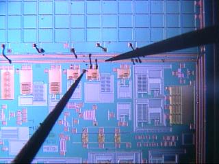
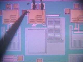
35 Integrated Device
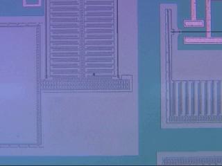
36 Integrated Device
37 Process Limitations NMOS only capabilities Transistor breakdown voltages ~27 V
38 Second generation CMOS process Design focus Improved circuit performance Self-aligned, polysilicon gates CMOS circuit capabilities Higher breakdown voltage Better control of threshold voltages Isolation trenches etched and back-filled after solar cell and circuit fabrication Meet specific project needs
39 Second generation CMOS process SmartDust Integrated solar cell arrays and electrostatic actuators

40 Second generation CMOS process Microrobots Integrated solar cell arrays and high-voltage buffers
41 Results CMOS capabilities allow for more sophisticated buffers Voltage translator circuit using a variant of a cross coupled inverter
42 Conclusions Integrated process has been developed including High voltage solar cell arrays High aspect ratio electrostatic actuators High voltage buffers Integrated device fabricated in the process has been demonstrated Second generation process has been developed solving the most significant process limitations
43 Acknowledgements SmartDust and Microrobot projects at UC Berkeley Prof. A.P. Pisano Prof. K.S.J. Pister Staff of the Berkeley Microfabrication Laboratory