Materials: Structures and Synthesis
|
|
|
- Raymond Stewart Copeland
- 5 years ago
- Views:
Transcription


1 微纳光电子材料与器件工艺原理 Materials: Structures and Synthesis Xing Sheng 盛兴 Department of Electronic Engineering Tsinghua University 1

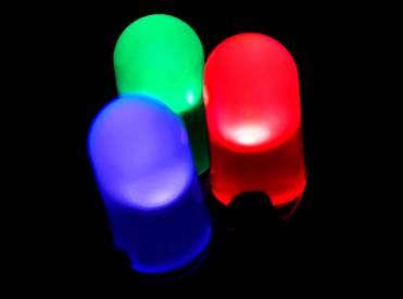


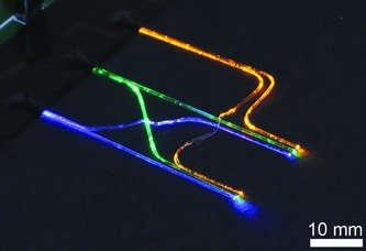

2 Optical and Electronic Devices LEDs lasers waveguides fibers detectors solar cells metamaterials photonic crystals integrated circuits 4


3 Raw Materials MOS: Metal-Oxide-Semiconductor Silicon SiO 2 Metal 6

4 Crystal Structures video 7
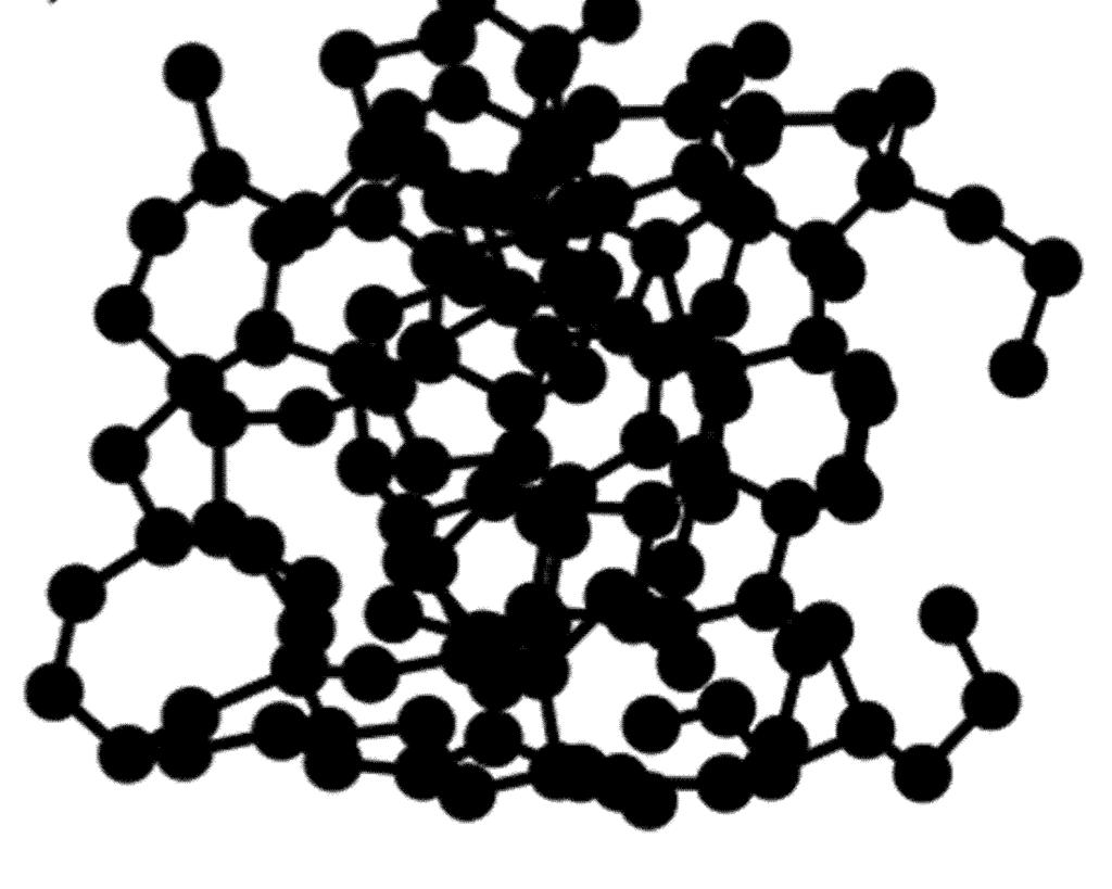
5 It is all about energy Lennard-Jones Potential V ( r) A r 12 B 6 r video 8

6 Crystal Structures Li, Na, Cr,... Al, Cu, Au,... Mg, Zn, Ti,... 3D: 14 Bravais lattices 32 point groups 230 space groups 9

7 Miller Indices (lmn) plane intercepts at a 1 /l, a 2 /m, a 3 /n 10
8 Exercise in class draw planes below (120), (112), (131) (lmn) plane z intercepts at a 1 /l, a 2 /m, a 3 /n x y 11
9 Defects in Crystals Q: why? 0D point defect 1D dislocation 2D grain boundary 12


10 Single Crystal (Mono Crystal) Xing Sheng, Quartz Sugar Silicon wafers, GaAs, GaN, sapphire,... turbine blade 13
11 Polycrystal Q: why blue? grain boundary polycrystalline silicon metal ceramic 14


12 Amorphous Materials Xing Sheng, Defects are everywhere... silica fiber glass Q: why is glass transparent? plastics 15


13 Carbon diamond graphite amorphous carbon Q: which one is electrically conductive, diamond or graphite? 16

 graphene A.")
14 Carbon H. Kroto, R. Curl, R. Smalley 1996 Nobel Prize in Chemistry carbon nanotube S. Iijima, Nature 354, 56 (1991) graphene A. Geim, K. Novoselov 2010 Nobel Prize in Physics 17

")
15 2D Materials Single atomic layer crystal graphene A. Geim, K. Novoselov 2010 Nobel Prize in Physics Transition metal dichalcogenide (TMDC) MoS 2, WSe 2,... 18


16 Liquid Crystals Liquid crystal display (LCD) P. de Gennes 1991 Nobel Prize in Physics 19

17 Organic Materials Small Molecules OLED 20

18 Organic Materials LCD vs. OLED 21


19 Organic Materials Polymers 22


20 Quasi-Crystal Neither crystalline nor amorphous 5, 8, 10, or 12-fold symmetry Penrose tiling A Ho-Mg-Zn quasicrystal D. Shechtman 2011 Nobel Prize in Chemistry 23


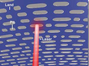
21 Optical Disc Phase Change Memory 24


22 Materials Characterization HRTEM High Resolution Transmission Electron Microscope amorphous single crystal quantum dot 25


23 Materials Characterization HRTEM High Resolution Transmission Electron Microscope diffraction patterns single crystal polycrystal amorphous 26

24 Materials Characterization XRD X-ray Diffraction 27
25 Materials Characterization DSC Differential Scanning Calorimetry Glass Transition Crystallization Melting 28
26 CMOS Device polycrystalline amorphous single crystalline Silicon SiO 2 Metal 29
27 Substrates for Devices Xing Sheng, Usually single crystals (why?) diamond structure: Si, Ge, C,... 30

 amorphous")
28 Substrates for Devices Xing Sheng, quartz (SiO 2 ) amorphous glass 31


29 Substrates for Devices Xing Sheng, zinc blende structure: GaAs, InP, -SiC,... Wurtzite structure: -SiC, GaN, ZnO,... sapphire (Al 2 O 3 ) 32


30 Lattice Constants vs. Bandgap 33
31 Requirement for Electronics low cost single crystal p-doping and n-doping low defect level purity > % dislocation < 1000 /cm 2 suitable bandgap too large -> high voltage, power,... too small -> thermal noise, leakage, defects,... semiconductor/oxide interface quality mobility, surface uniformity,... Xing Sheng, EE@Tsinghua 34
32 Silicon vs. Germanium Xing Sheng, Silicon earth abundant > 25% on earth perfect Si/SiO 2 interface bandgap 1.1 ev vs. Germanium expensive GeO 2 is not stable bandgap 0.67 ev Silicon wins and will always win (?) 35
33 Properties of Silicon Xing Sheng, Structural diamond structure (FCC) lattice constant a = Å atomic density = /cm 3 melting point = 1417 C a Electronic bandgap E g = 1.12 ev dielectric constant r = 11.9 mobility: electron e = 1500 cm 2 /V/s, hole h = 450 cm 2 /V/s intrinsic carrier density n i = /cm 3 Optical refractive index n = 3.6 absorbs < 1100 nm, transparent > 1100 nm 36

34 How to Make Silicon Wafers? Xing Sheng, Video SiO 2 raw Si IC chips Si ingots and wafers 37
35 How to Make Silicon Wafers? Xing Sheng, SiO 2 raw Si SiO 2 + 2C = Si + 2CO at 2000 o C Metallurgical Grade Silicon, purity ~ 98% Applications: aluminum, silicone,... 38
36 How to Make Silicon Wafers? Xing Sheng, SiO 2 raw Si Si + 4HCl = SiCl 4 + 2H 2 SiCl 4 + 2H 2 = Si + 4HCl purification (Siemens process) Polycrystalline Silicon, purity > 99.99% Applications: solar cells,... 39
37 How to Make Silicon Wafers? poly crystal -> single crystal Xing Sheng, Czochralski process (CZ) Float-zone process (FZ) raw Si Si ingots and wafers 40

")
38 How to Make Silicon Wafers? Xing Sheng, Czochralski process (CZ) Float-zone process (FZ) 41


39 How to Make Silicon Wafers? Xing Sheng, wafer slicing wafer polishing 42


40 Silicon wafers: size 4 inch 6 inch 8 inch 12 inch 18 inch 18 inch wafer 43
41 Silicon wafers: purity Xing Sheng, Metallurgical grade polycrystalline purity > 98% application: aluminum alloy, silicone Solar grade polycrystalline purity > 99.99% (4N) application: solar cells Electronic grade single crystalline purity > % (9N) application: IC industry, high efficiency solar cells 44

42 Silicon wafers: defects Xing Sheng, 45

43 Silicon wafers: doping Xing Sheng, 46

44 Silicon wafers: orientation Xing Sheng, cleavage direction why??? 47

45 Breaking Amorphous Materials 48
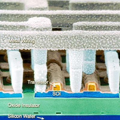

46 Silicon-on-Insulator (SOI) Xing Sheng, 49

47 Silicon-on-Insulator (SOI) Xing Sheng, Silicon waveguide Ring resonator 50


48 Other single crystals Xing Sheng, Ge GaAs sapphire Q: Can we make diamond crystal? 51
 2009 Nobel Prize")

49 Optical Fibers K. Kao ( 高锟 ) 2009 Nobel Prize in Physics K. C. Kao, G. A. Hockham, Proc. IEE 113, 1151 (1966) 52

50 Absorption of Silica (SiO 2 ) Xing Sheng, EE@Tsinghua minimum loss at 1550 nm, 0.2 db/km ~ 2% loss every kilometer 53


51 preform Optical Fiber Drawing Xing Sheng, fibers Video 54


52 Glass Transition 吹 玻璃 1st order tansistion 2nd order tansistion glassy / plastic state viscous / rubbery state 55


53 Optical Fibers 56
54 Thank you for your attention 59