Semiconductor device fabrication
|
|
|
- Cody Perkins
- 5 years ago
- Views:
Transcription
1 REVIEW
2 Semiconductor device fabrication is the process used to create the integrated circuits (silicon chips) that are present in everyday electrical and electronic devices. It is a multiplestep sequence of photographic and chemical processing steps during which electronic circuits are gradually created on a wafer made of pure semiconducting material. Silicon is the most commonly used semiconductor material today, along with various compound semiconductors. The entire manufacturing process, from start to packaged chips ready for shipment, takes six to eight weeks and is performed in highly specialized facilities referred to as fabs. How many fabs are there in India? In India: Semiconductor Complex (SCL) Chandigarh DRDO, ISRO, BEL have facilities Source: Wikipedia
3 Now, we will see, by photographs, the entire process sequence! Sand With about 25% (mass) Silicon is after Oxygen the second most common element in the earth's crust. Sand especially Quartz - has high percentages of Silicon in the form of Silicon dioxide (SiO2) and is the base ingredient for semiconductor manufacturing. Source: INTEL

4 Melted Silicon Silicon is purified in multiple steps to finally reach semiconductor manufacturing quality which is called Electronic Grade Silicon. Electronic Grade Silicon may only have one alien atom every one billion Silicon atoms. In this picture you can see how one big crystal is grown from the purified silicon melt. The resulting mono crystal is called Ingot. Polycrystalline silicon, also called polysilicon, or simply Poly, is a material consisting of small silicon crystals or crystallites. The structure is different from single-crystal silicon, used for electronics and solar cells, and from amorphous silicon, used for thin film devices and solar cells. Source: INTEL
5 Source: INTEL Mono-crystal Silicon Ingot An ingot has been produced from Electronic Grade Silicon. One ingot weights about 100 kilograms (=220 pounds) and has a Silicon purity of %

6 Ingot Slicing The Ingot is cut into individual silicon discs called wafers. Thickness is also very important warpage grinding rigidity Source: INTEL
7 Source: INTEL Wafer The wafers are polished until they have flawless, mirror-smooth surfaces. Intel buys those manufacturing ready wafers from third party companies. Intel s highly advanced 45nm High-K/Metal Gate process uses wafers with a diameter of 300 millimeter (~12 inches). When Intel first began making chips, the company printed circuits on 2-inch (50mm) wafers. Now the company uses 300mm wafers, resulting in decreased costs per chip.
8 Applying Photo Resist The liquid (blue here) that s poured onto the wafer while it spins is a photo resist finish similar as the one known from film photography. The wafer spins during this step to allow very thin and even application of this photo resist layer. Coating methods? Source: INTEL
9 Source: INTEL Exposure The photo resist finish is exposed to ultra violet (UV) light. The chemical reaction triggered by that process step is similar to what happens to film material in a film camera the moment you press the shutter button. The photo resist finish that s exposed to UV light will become soluble. The exposure is done using masks that act like stencils in this process step. When used with UV light, masks create the various circuit patterns on each layer of the microprocessor. A lens (middle) reduces the mask s image. So what gets printed on the wafer is typically four times smaller linearly than the mask s pattern.

10 Exposure Although usually hundreds of microprocessors are built on a single wafer, this picture story will only focus on a small piece of a microprocessor from now on on a transistor or parts thereof. A transistor acts as a switch, controlling the flow of electrical current in a computer chip. Intel researchers have developed transistors so small that about 30 million of them could fit on the head of a pin. Source: INTEL Other advanced exposure methods?
11 Washing off of Photo Resist The unexposed photo resist is completely dissolved by a solvent. This reveals a pattern of photo resist made by the mask. Source: INTEL Types of photoresist Dry, Wet Positive, Negative Developers Rinse with deionized water Dry
12 Etchant material types of etchant dry (plasma, RIE), wet (chemical) Resolution after etching Isotropic and Anisotropic etching For Si- KOH etchant Etching The photo resist is protecting material that should not be etched away. Revealed material will be etched away with chemicals. Source: INTEL
13 Removing Photo Resist After the etching the photo resist is removed and the desired shape becomes visible. Resist Strippers Aqueous No residues Inspection for residues Source: INTEL
14 Source: INTEL Applying Photo Resist (for Doping or Ion Implantation) There s photo resist (blue color) applied, exposed and exposed photo resist is being washed off before the next step. The photo resist will protect material that should not get ions implanted.
15 Source: INTEL Ion Implantation Through a process called ion implantation (one form of a process called doping), the exposed areas of the silicon wafer are bombarded with various chemical impurities called Ions. Ions are implanted in the silicon wafer to alter the way silicon in these areas conducts electricity. Ions are shot onto the surface of the wafer at very high speed. An electrical field accelerates the ions to a speed of over 300,000 km/h (~185,000 mph)
16 Source: INTEL Removing Photo Resist After the ion implantation the photo resist will be removed and the material that should have been doped (green) has alien atoms implanted now (notice slight variations in color)
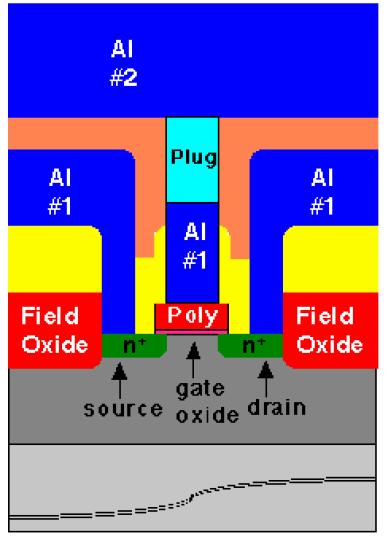
17 Source: INTEL Ready Transistor This transistor is close to being finished. Three holes have been etched into the insulation layer (magenta color) above the transistor. These three holes will be filled with copper which will make up the connections to other transistors.
18 Electroplating The wafers are put into a copper sulphate solution as this stage. The copper ions are deposited onto the transistor thru a process called electroplating. The copper ions travel from the positive terminal (anode) to the negative terminal (cathode) which is represented by the wafer. Other deposition methods? Source: INTEL
19 After Electroplating On the wafer surface the copper ions settle as a thin layer of copper. Metallization can also be done by CVD, evaporation or sputtering Source: INTEL

20 Source: infras.com
21 Source: INTEL Polishing The excess material is polished off.

22 Source: infras.com
.")
23 Source: INTEL Metal Layers Multiple metal layers are created to interconnect (think: wires) in between the various transistors. How these connections have to be wired is determined by the architecture and design teams that develop the functionality of the respective processor (e.g. Intel Core i7 Processor ). While computer chips look extremely flat, they may actually have over 20 layers to form complex circuitry. If you look at a magnified view of a chip, you will see an intricate network of circuit lines and transistors that look like a futuristic, multi-layered highway system. Use of microvias will be essential for creating multilayers.
24 Wafer Sort Test This fraction of a ready wafer is being put to a first functionality test. In this stage test patterns are fed into every single chip and the response from the chip monitored and compared to the right answer. Electrical Probe Test/Flying probe test Source: INTEL
25 Wafer Slicing The wafer is cut into pieces (called dies). Diamond saw is used Slicing along the scribe areas Source: INTEL
26 Discarding faulty Dies The dies that responded with the right answer to the test pattern will be put forward for the next step (packaging). Sort out KGDs- Known Good Die Source: INTEL
. The die shown here is a die of an Intel Core i7 Processor.")
27 Individual Die This is an individual die which has been cut out in the previous step (slicing). The die shown here is a die of an Intel Core i7 Processor. Source: INTEL
28 Inspection & Measurement! Multiple Inspection points throughout the Process: " Reticle and Mask Inspection " Wafer Inspection " Metrology/Critical Dimensions " Defect Inspection " Parametric! Critical Issues " Finer Geometries " Volumes of Data " Process Control