Organic Light-Emitting Diodes. By: Sanjay Tiwari
|
|
|
- Debra Stephens
- 5 years ago
- Views:
Transcription
1 Organic Light-Emitting Diodes By: Sanjay Tiwari

2
3
4 Inorganic Vs. Organic Material Properties
5 Limitations At Early Stage Organic materials have often proved to be unstable. Making reliable electrical contacts to organic thin films is difficult. When exposed to air, water, or ultraviolet light, their electronic properties can degrade rapidly. The low carrier mobilities characteristic of organic materials obviates their use in highfrequency (greater than 10 MHz) applications. These shortcomings are compounded by the difficulty of both purifying and doping the materials.
6

7
8

9

10
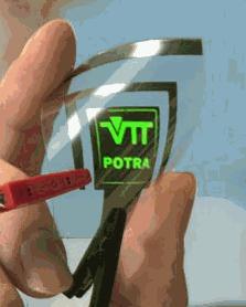
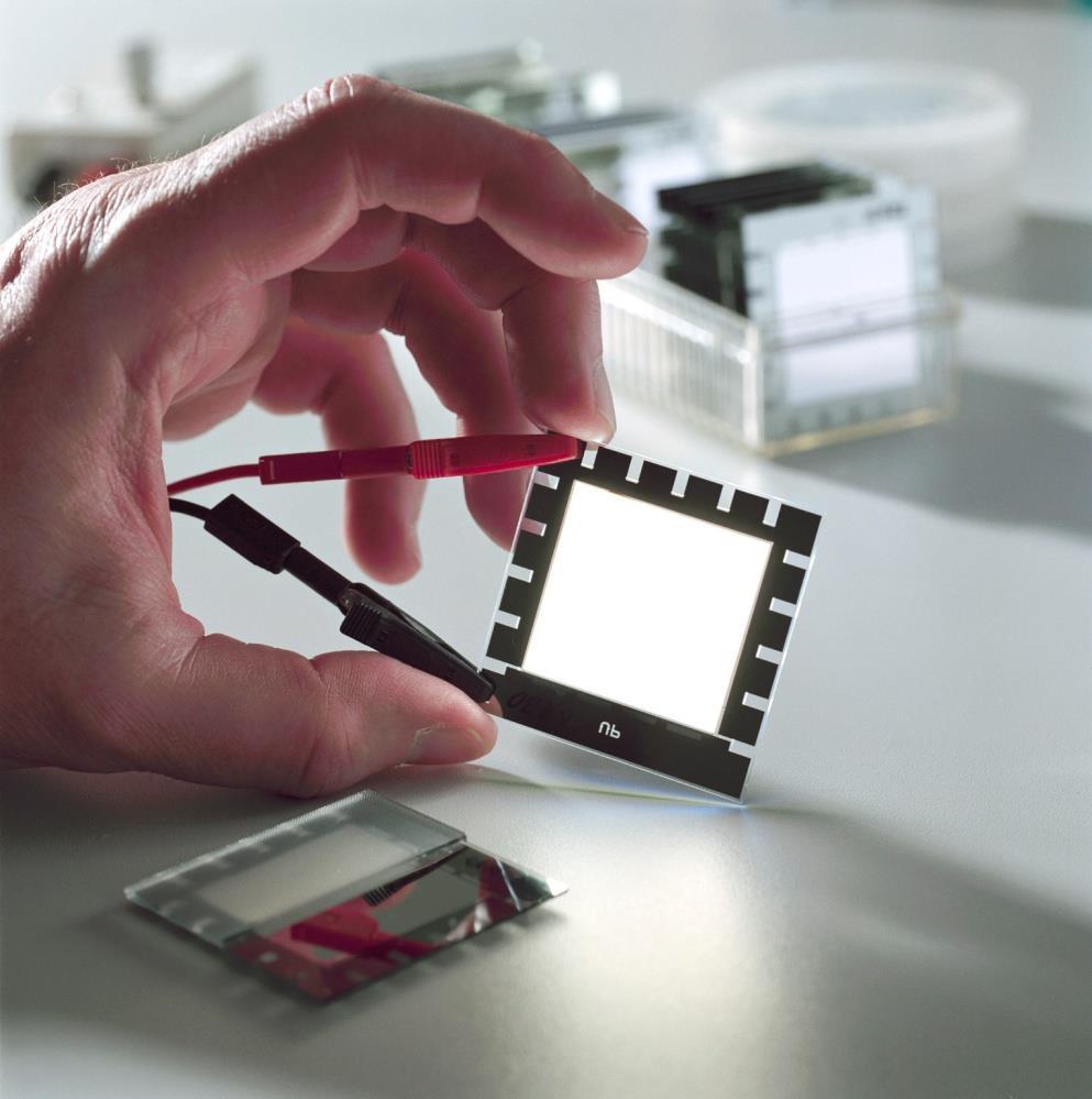
11 What is an OLED? An OLED is an electronic device made by placing a series of organic thin films between two conductors. When electrical current is applied, a bright light is emitted. A device that is 100 to 500 nanometers thick or about 200 times smaller than a human hair.

12

13
![Polymer Light Emitting Diode Cathode: Metal (0.1 0.5 mm) [Ca, Mg/Al] Polymer (~ 0.1 mm) Curtesy: R. H.](/docs-images/89/98239774/images/14-0.jpg "Friend Glass or PET (10 mm 5 mm) Anode: Indium-Tin Oxide (0.1 0.3 mm) transparent, e.g.")
14 Polymer Light Emitting Diode Cathode: Metal ( mm) [Ca, Mg/Al] Polymer (~ 0.1 mm) Curtesy: R. H. Friend Glass or PET (10 mm 5 mm) Anode: Indium-Tin Oxide ( mm) transparent, e.g., in LCDs The active part is very thin (< 1 mm)
15 Polymer Light Emitting Diode Polymer LED Conduction band ITO V Metal cathodes Polymer Glass substrate ITO h + e - Metal hn Valence band J.H. Burroughes, et al, Nature p539


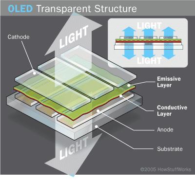
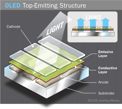
16 The OLED Structure

17 How OLEDs Emit Light The battery or power supply of the device containing the OLED applies a voltage across the OLED. An electrical current flows from the cathode to the anode through the organic layers. (an electrical current is a flow ( electrons of At the boundary between the emissive and the conductive layers, electrons find electron holes. The OLED emits light.
18

19
20 Polymer Light Emitting Diode Polymer LED V Metal cathodes Cathode Interface Metal Diffusion Introduction of Impurities Barrier - poor e - injection Polymer ITO Glass substrate Anode (ITO) Interface Indium, Oxygen Diffusion Barrier poor h + injection Variations in morphology Variations in work function
21

22

23

24
25
26

27
28 Types of OLEDs Passive-matrix Active-matrix Transparent Top-emitting Flexible White
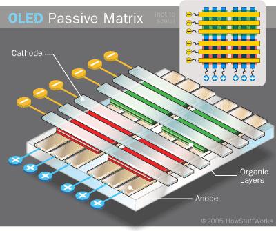


29 Passive-Matrix


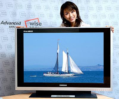
30 Active-Matrix


31 Transparent

32 Top-Emitting


33 Flexible


34 White
35 Advantages Thinner, lighter and more flexible Brighter Consume much less power Easier to produce and make into larger sizes Large field of view
36 Disadvantages Lifetime Manufacturing Water

37 Current OLEDs


38 Future of OLEDs?

39
40

41

42
43
44
45

46
47

48
49
50
51
52

53 Inorganic Vs. Organic LEDs
54 Molecular Orbitals
55 Organic LED Energy Diagram
56

57

58
 Organic material Organic")
59 Organic Thin Film Transistors (OTFTs) Organic material Organic material
60 An Example of an I-V of OTFTs Lg = 20 µm W = 220 µm 400 nm SiO 2 50 nm organic
61
62 Simulation to charge injection and transport in OLED
63 1. motivation outline 2. Charge injection issue 3. Overview of charge injection 4. Charge transport 5. Experiment & Simulation 6. Conclusion Simulation to charge injection and transport in OLED
64 Motivation of development of organic electronic devices low cost and various kinds of substrate Traditional devices restrict to silicon substrate, though with a better performance. Attractive application: the novel flat-panel display technology based on OLED.
65 Obstacles Research difficulties : Complexity of interface Hard to experimentally measure trap distribution Necessity: electrical contact with other components significant issue if new material Goal: To overcome energy barrier.
66 Overview of Charge injection
67 Early theories Fowler-Nordheim theory & Richard-Schottky theory fail to consider the amorphous nature of the organic. Amorphous, not crystalline Organic, not semiconductor However, J mobility & DOS Monti-Carlo Simulation (1993)
68 Energy diagram of RS & FN

69 Theory in 2003 the barrier height the image potential applied voltage disorder
70 Charge transport
71 2 characteristics of OLED insulator Eg large->n 0 very small V large -> n i large When n i >>n 0 -> SCLC Disorder Molecule, not lattice Poole-Frenkel effect
/(v/cm)")
72 Murgatroyd vs. Barbe L=1e-5; %cm u=1e-5; % (cm/s)/(v/cm) die=5*8.85e-14; %F/cm V=0.5; T=27~150 C
73 Experiment & simulation


74 Experiment Goal: Work ft dependence of OLED Check temperature dependence of OLED Device structure: Al/Alq/various cathodes Not aim to light Data: Not yet

75 simulation SCLC + Frenkel + thermal carrier
76 Conclusion & future work While SCLC theory has describe charge transport very well, a comprehensive theory to charge injection is needed. For transport, find out the Temperature dependence. For injection, find out the work function dependence.
77 reference 1. M. A. Baldo and S. R. Forrest PHYSICAL REVIEW B, VOLUME 64, J. Campbell Scott J. Vac. Sci. Technol. A M. A. Lampert, current injection in solids