Optimizing the Insulated Metal Substrate Application with Proper Material Selection and Circuit Fabrication
|
|
|
- Richard Edwards
- 5 years ago
- Views:
Transcription
1 Abstract Optimizing the Insulated Metal Substrate Application with Proper Material Selection and Circuit Fabrication Dave Sommervold, Chris Parker, Steve Taylor, Garry Wexler. The Bergquist Company Prescott, WI The ever expanding growth in the use of insulated metal substrates (IMS) in power electronics requires a focus on material and mechanical configuration for each application. By optimizing the material makeup and printed board format, performance and reliability expectations can be further achieved. The thermal performance and electrical isolation needs are driven by the power requirements, but considerations of temperature range, mechanical durability and format, along with the physical package surrounding the substrate must also be managed. With a variety of material configurations and circuit format capabilities, the choices become a balancing of options to maximize performance and minimizing cost through Design For Manufacturability (DFM) in the circuit board fabrication. These challenges present the IMS printed board fabricator with material selections and fabrication processes unlike those for other printed board or ceramic applications. Introduction With the enormous growth of (IMS) used in LED lighting, automotive applications, power conversion, motor drives and semiconductor modules the complexity of the designs will require proper material selection and optimized circuit fabrication processes. Designs have gone beyond the basic platform to mount specific devices that need thermally efficiency. Critical control of maximum junction temperatures and power densities require optimum thermal performance. Electrical isolation requirements will continue to vary, but most applications will continue to require safety agency testing at higher than operating voltages. Thus the importance of proper material selection, including type of base substrate, dielectric thermal performance and thickness, along with circuit foil weight cannot be lightly considered. Lastly the extreme cost sensitivity of all the components in the application requires realistic expectations from the printed board fabrication and the (DFM) process be utilized throughout the design, from printed board fabrication through printed board assembly. There is also the importance of proper safety agency recognitions, RoHS and REACH compliance, along with the need for Pb-free assembly processes. Material Selections Making the major decision as to what use for IMS substrate printed board is much more than finding a thermal solution. The selection of materials from base substrate material to dielectric type to foil weight will have significant outcome on the design and its ability to meet performance requirements and fulfill the challenges of reliability in the applications operating environment. The construction of these composite materials forces considerations of thermal-mechanical effects not only on substrate material, but also on the components mounted to the circuit board. The most common base material in use today is aluminum, but underwater lightning applications require a copper base metal. As the power requirements continue to increase, the circuit copper increase in thickness to support the amperage needs. The copper/dielectric/aluminum composite are more heavily affected by differences in Coefficient of Thermal Expansion (CTE). A general Rule-of-Thumb has been as the copper foil thickness becomes greater than 10% of the base aluminum thick, not only is CTE effects during temperature cycling an issue, but printed board overall flatness becomes a real challenge. That is to maximize the thermal transfer to a heatsink full contact must be made, air gaps are not acceptable. Cte Effects Differences in CTE in composite materials can dramatically affect reliability in applications that have a large operating temperature range. This CTE mismatch can mechanically stress the design causing solder joint fatigue and component fracture. As a result, the choice of base metals needs to be carefully considered. Choosing copper base material instead of aluminum has emerged as a popular solution to the requirements of heavy weight copper foil as devices need to carry more and more power. With a copper base, the foil and base metals are the same resulting in considerably reduced stress in the composite, although at a cost. Copper is more expensive than aluminum and often requires additional processing to meet all of the product requirements. The difficulty in bonding dielectric to wrought copper has limited suppliers, and the copper base substrate usually requires a robust protective finish to prevent corrosion, such as nickel plating. Emerging materials such as Aluminum-silicon carbide (AlSiC) metal matrix composites can address the CTE mismatch issues and the costly process of surface protection of the bare copper.
2 Dielectric Considerations The choice of dielectric materials should focus on Thermal Impedance, Dielectric Strength and Glass Transition Temperature (Tg). There seems to be a common misunderstanding of these characteristics by most initial users of IMS. Yes, thermal conductivity, as expressed as W/mK is important. But thinner dielectrics, with the same bulk conductivity, will have improved thermal impedance. Conversely, thicker materials will have increased thermal impedance. IMS Thermal Impedance is really what is important: which also includes the interfacial resistance in the layers of the composite. This combined with the solder joint and the device should be a very important consideration to the designer. The overall thermal impedance combined with that of the operating device will determine the junction temperature at a power level in the ambient temperature operated. Solely focusing on thermal conductivity can be deceptive when trying to determine the true performance of the substrate. The understanding of thermal impedance is needed when comparing to pure ceramic substrates, such as direct bond copper (DBC) or Thick-Film. Although these materials have a much higher thermal conductivity than IMS, their overall substrate thickness yields thermal resistance values very similar to high performance IMS substrates. Glass Transition Temperature (Tg) A common misconception is the concern of operating IMS above the Tg of the dielectric. Above the Tg of the material, mechanical and electrical properties begin to change. Mechanical changes of note are reduction of peel strength of the copper foil, an increase in the CTE, and decreasing storage modulus. Due to the ceramic-polymer blend dielectrics in IMS, the absence of glass, and the thinness of the dielectric layer, strain from Z-axis expansion is significantly reduced. With these very thin dielectrics, the base metal material is totally dominant in the composite. There is a real potential benefit of relieving residual stress on the dielectric interfaces, in solder joints, and other interconnects due to CTE mismatches by choosing a dielectric with Tg below the operating temperature. This is because the dielectric material above Tg is in its elastomeric state (much lower storage modulus) allowing some of the stresses to relax. Changes in electrical properties must also be considered in operation above Tg, although they commonly are only important at frequencies above 1 MHz. Effects to consider are changes in the permittivity, dielectric loss and breakdown strength of the material. Another key note here is that most available IMS substrates have a Tg in the 105 C range, but some have UL maximum operating temperatures of 130 C or greater. This is really not an issue in LED lighting applications where 95 C is the maximum junction operation temperature. Operating above the UL MOT limit will cause a reduction in the electrical and mechanical performance characteristics over the 100,000-hour life prediction. Current Capacity Copper foil weight is a very important consideration in the design. The copper foil thickness needed to meet current requirements and the effective heat spreading needed for the devices must be considered. Additional current that can be accommodated by IMS is due to its ability to spread and dissipate the heat generated by I 2 R losses this is shown in figure 1. Figure 1 Heat Spreading The dielectric thickness and foil thickness both influence the heat spreading capability of IMS and it is one of the most powerful advantages derived from IMS. By increasing copper conductor thickness, heat spreading increases and brings
3 device temperature down, along with I 2 R losses in the copper traces. This allows for much higher current carrying ability with IMS over FR4, because of the ability to dissipate heat due to the I 2 R loss in the copper circuitry. Heat Spreading Figure 2 Current Capability The heat spreading capability of the IMS is also very important. Both the copper thickness and dielectric thickness influence the heat spreading. The ability to increase the heat spreading brings junction temperatures down to enable higher power and increase reliability. As shown in figure 5, increasing copper thickness decreases the representative power device case temperature. The importance of this cannot be overstated with respect to available power and long-term reliability. As a rule of thumb, a two-fold increase in mean time between failures (MTBF) can be realized with a 10 C reduction in junction temperature. This has been most evident in the rapid adoption of IMS in almost all LED lighting applications. Metal Base The selection of IMS base layer metal and thickness is application specific. Aluminum is the most commonly used material, and the alloy is primarily driven by fabrication method. Alloy 6061 T6 is the most machinable, but if forming is required, a softer alloy like 5052 H34 is recommended. The thickness of the base metal is driven by mechanical rigidity requirements, mechanical fasteners (Press-Fit), other machining, such as threaded-holes, need for thermal mass and in many cases price. The high-volume DC-DC market has chosen the thinner base materials, due to price. The motor drive markets typically choose thicker materials for thermal mass and mechanical rigidity. The LED applications chose the thinner aluminum materials primarily to reduce cost, except in very high performance applications where copper is the choice. In these applications, where die are directly attached the use of thicker aluminum bases or a copper base is common, with base materials up to.125 inches thick. A capability seeing more and more use is the ability to directly solder to or make platedthrough connects on a copper base substrate or ablated openings to allow direct attachment to the copper metal base. There is a process that allows coplanar metal base attachment, such as pedestals. This is obviously not possible on thin aluminum. Although press-in hardware has been successfully used to make base connections, designs where the dielectric is ablated away and a connection is ultrasonically welded to the base aluminum has been used successfully. Other specialty materials are available as base material as well, depending on the need for magnetic properties, specific CTE ranges, or other properties. This broad offering of base material metals and thickness allows the designer to tailor the design to the application requirements. This flexibility in the IMS allows its use to go beyond just a component mounting and interconnect platform. The IMS material selections give the designer the ability to minimize thermal resistance, maximize electrical isolation needs, and optimize the copper circuit thickness for current requirements and/or heat spreading and the optimum baseplate to package the application. Safety Agency Testing Considerations
4 Often the designer will choose the thinnest material possible to optimize thermal performance at the expense of those required distances. Published dielectric breakdown values are generally material properties tested in lab conditions and not directly applicable to specific designs. Furthermore the breakdown voltage is the voltage at which the dielectric breaks down, and not appropriate as a test voltage. So, the designer needs to consider the isolation needed to pass testing without degradation to the dielectric or test faults. The small increases in dielectric thickness needed to provide electrical safety test margin do not necessarily cause detrimental affects to thermal performance. It is critical that voltage isolation distances required in safety agency standards are considered when using IMS materials. The printed board fabricator really cannot determine the proper Creepage Clearance requirements; only the designer can determine the clearance required for reliable testing and operation. It is the fabricators responsibility to use proper recognized materials and printed board recognitions to meet the customer requirements of their safety agency requirements. Circuit Fabrication Although similar to the circuit processing done to produce FR-4 PWB s, IMS fabrication really differs at the final singulation or depanelization stage; separating the individual boards from the panel. The initial steps of imaging, etching, soldermask and surface finishing uses the similar type of equipment and processing as FR-4. Where as most FR-4 boards are double-sided or multi-layer constructions, IMS is single-sided and process methods to protect the base-side must be utilized. The primary design consideration for manufacturability is that IMS boards are built using heavier copper weights for high power applications. The average copper weight is typically 4 oz, with many designs on 6oz to 10oz. Due to these copper weights the board layout must allow for the etching characteristics of the heavy copper. The typical LED application is primarily 2 oz, but finer line and spaces are typical, with a significant amount of fill copper to enhance heat spreading. The process capability of the fabricator varies slightly, but the design rule check (DRC) requirements take into account the minimum trace spacing and width. Thus the board layout must take into consideration the larger spacing between features; such as for 4oz to for 10oz and minimum widths of for 4oz and for 10oz. Thus the ability to place finer pitch components and the needed SMD power devices on the same circuit board may not be possible. This is seen in the typical approach used for DC-DC converters; the power devices are mounted to the IMS board and the finer pitch devices are on a multi-layer FR-4 board attached above using SMD interconnect pins. Heavy Copper Foil With the need for the heavy copper to support current and heat spreading requirements, other process considerations must be addressed. The application of soldermask requires process optimization to allow adequate coverage both between the circuits and on the edge of the traces. This is due to the height of the thick copper and the ability to screen the soldermask down into the valleys, but yet have the proper thixotropic properties to remain on the edge or knee of the trace. Also another consideration in soldermask coverage is the recommendation to aperture the solder pads. The need to maintain Ionic cleanliness is critical for long-term reliability. To ensure the cleanliness after reflow having soldermask coverage on the edge of pads eliminates flux residuals from being trapped in the corners and causing future contamination that could lead to a latent field failure. With this recommendation in mind, DRC will check to verify enough overlap had been designed into the aperture to maintain good soldermask adhesion through subsequent processes. With IMS used in many direct die attachment applications, soldermask is often used as a solder dam. The design consideration here is minimum line width to again maintain soldermask adhesion through plating and reflow soldering processes. Board designers should also consider soldermask compatibility in their application, as many IMS boards end up in modules that require potting compounds or conformal coating. As in plating requirements, soldermasks are different by supplier and should be verified for compatibility to processes. Another design consideration with the heavy copper features involves boards requiring Legend or silk-screen. As this is also a screening process, the height of the copper and placement of characters or features must be considered in the layout. This includes the bridging of characters or features across copper circuits and the relationship to the edge of the finished part. This problem can be elevated with the use of digital printing of the Legend in most cases, but it is mostly limited to white only, currently. Surface Finish The surface finish requirements for IMS boards are also similar to those of FR-4 boards, but circuit features are usually much larger, due to the power devices. This does affect final thickness variations on HASL finishes, due to the feature sizes. Maintaining adequate thickness on large pads will cause greater thickness on small pads. Process optimization is required by the fabricator to balance the thickness across feature sizes. In plating requirements, such as ENIG and ENEPIG used in aluminum and gold wire-bond applications, the fabricator has to isolate the base metal from the plating process. The applications requiring such plating need to consider the pricing of the surface finish square inch, so plated area should be kept to a minimum using soldermask. The other surface finishes commonly used to provide good solderable surfaces are

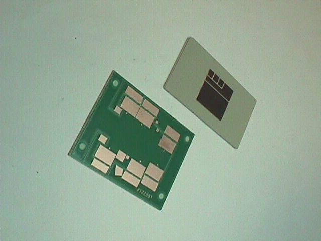
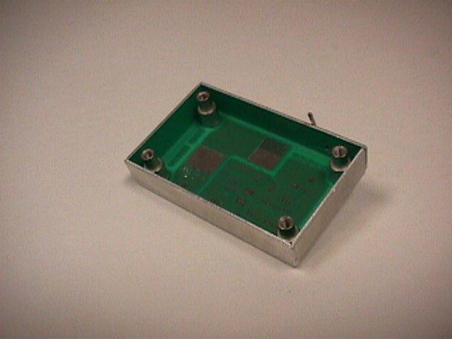
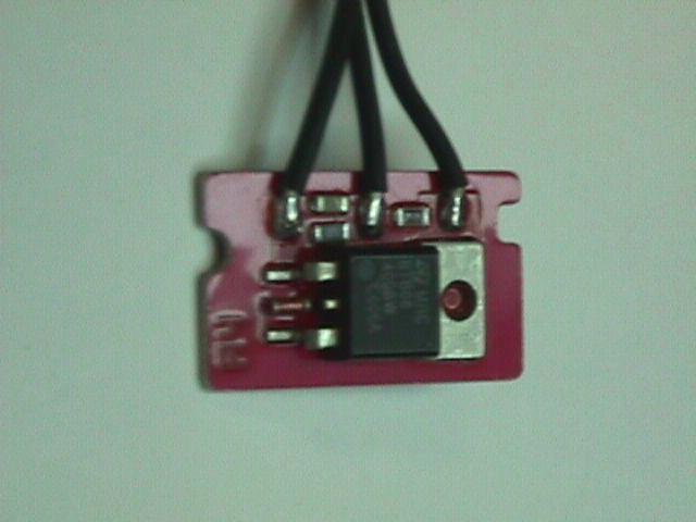
5 organic solderability protect ant s (OSP), but these due have shorter shelf lives and require more careful handling during assembly. The use of immersion tin and silver has seen volume production. It has been extensively used on boards with a copper base metal, to surface finish the circuits for solderability and the base to prevent copper oxidation. These types of surface finish also require similar careful handling and packaging to prevent corrosion. Surface finishes can also include those for the metal base side of the IMS substrate; these include anodization and conversion coating for aluminum and plating for the copper. Depending on the part requirement this can be done in panel form or at the individual part level. If the part requires coverage on the edges this finishing process must be done on the singulated part. It should be realized the price for individually surface finished parts is substantial higher in price than one done in panel form due to handling labor. Addition Of Holes/Slots Drilling, which is considered routine for FR-4 material is much different for IMS substrates. Drilling ceramic filled polymer with usually a thick metal base, definitely affects holes size capability and drill bit life. Typically, hole sizes vary from diameter for plated through vias to diameter for non-plated mounting holes. In the case of larger holes, a pilot hole is required. Also a deburring step is usually required, due to the exit burr at the metal base. The optimum method for large holes is to punch them. In a process comparison using a high-volume CNC punch press, the completed hole rate is 4 to 1 or more, over drilling. On higher volume applications this can be a significant price driver. A key factor to be remembered in IMS fabrication, final processes relate more to metal fabrication than they do to circuit board methods, but due to the dielectric materials; tooling and its maintenance is critical to overall fabrication quality. Therefore the use of technologies like carbide and diamond are essential.. Secondary Processes IMS substrates with its metal base can also have a number of other mechanical processes done, such as counter-sinks, counter-bores, threads, formed flanges and ablation of the dielectric material to expose the base metal for electrical connections. The designers need to consider the process capabilities of the fabricator. Tolerance and positional accuracy required affects type of process and final finished board yields, which directly influence price. These features, not available for ceramic and even FR-4 boards, can be provided by a proficient IMS fabricator at an acceptable price, in most cases. The use of mechanical fasteners is very common in IMS and not available for ceramics. Special processes that can be applied to meet specific application requirements include: selective dielectric removal, a pedestal, blind Via to metal base, via s both filled and unfilled and via in pad, as shown in figure 3.
6 Figure 3 Special Processes Singulation Final fabrication process methods significantly differentiate IMS from FR-4 or ceramic materials. This is the primary reason that only fabricators that have dedicated the process development time, and provided the necessary equipment to support the singulation process, have successfully processed IMS boards. The metal fabrication techniques and equipment required are critical for successful IMS fabrication. The V-scoring process similar to that used in the FR-4 world is used, but machine process speeds are very different and special metal cutting blades are necessary, along with the use of coolant to ensure sufficient tool life. The CNC capabilities of the machine allow for a variety of board geometries, but limit the board to a square or rectangle in most cases. It is also difficult in some cases to deal with the physical properties of the material, as it
7 relates to part flatness with this process. The v-scoring process does not influence the part; the part retains the character of the panel as it enters this cutting step. So, if the panel has a bow due to CTE mismatch of the copper and aluminum, the proportional bow will remain with the part. Although routing and milling are usually reserved for small volume or primarily prototypes, they remain singulation alternatives. The costs of these processes are extended machine times, tool wear, and typically require secondary deburring and cleaning operations. The advantage of these processes over v-scoring is the variety of PWB profile geometries that can be produced. IMS boards are possible in circular formats, to validate prototype designs. The milling process is also useful design verification for specialized array format designs. The combination of v-scoring and milling is useful in complex array formats as shown in figure 4. Figure 4 Fabrication combinations The preferred and most price competitive method to singulate IMS boards is punching. This method can generate board geometries in a vast variety of shapes and sizes. It is available for any of the material selections IMS has to offer. The only limiting factor is part size as it is related to tooling cost, but typical IMS boards are small in size. Using the same type of single-action and high- speed punch presses found in metal fabrication. The tool; punch/die sets are also very similar. The primary difference is in punch design to accommodate the exposed circuits on the IMS board. Punch relief is necessary to avoid punch contact with the circuitry, so there is no deformation of the copper into the dielectric. Any displacement of the copper and the dielectric can lead to a voltage breakdown fault, which renders the board defective. Due to this requirement, DRC rules require a minimum circuit-to-edge for the punch design. The minimum for aluminum is one material thickness. For copper-base boards this minimum has to be increased due to tensile strength of the material, to avoid fractures at the edge of the board. Tooling designs commonly employ multiple operations, such as piercing holes and profiling the perimeter. Progressive tools do have more front-end cost, but reduce the actual fabricated part price by reducing machine time and labor. The other option is CNC punch processes where a multiple number of tools can be loaded in the press to create the holes or slots required and the final perimeter punch of the PWB. It is also very cost effective in fabrication of complex arrays where a variety of shapes are required. This type of punch press can also create pedestal with special tooling. Another emerging process used on IMS boards is the forming of the metal. Utilizing the metal base as the fundamental platform IMS can be shaped into various requirements, including partial boxes, mounting flanges and other creative designs. Conclusions IMS substrates provide many advantages in power electronics and LED designs with the variety of material selections and circuit fabrication possibilities, examples shown in figure 5. The design does need to narrow down the choices of material configurations to meet performance and price requirements. Matching thermal performance, safety agency testing needs and best fabrication method can be greatly enhanced with a strong technical relationship with the material/fabricator vendor.


8 With the continued increases in power density and the exploding LED lightning market, more and more designers will have to look to IMS substrates for their applications needs. However the amount of differentiation from traditional FR-4 fabrication forces the need apply design practices not previously considered.

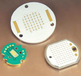
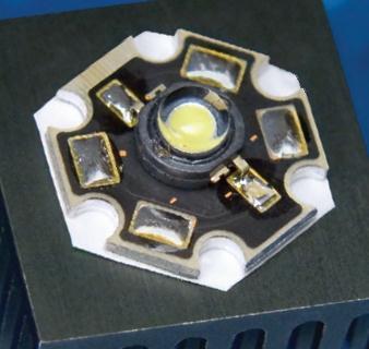
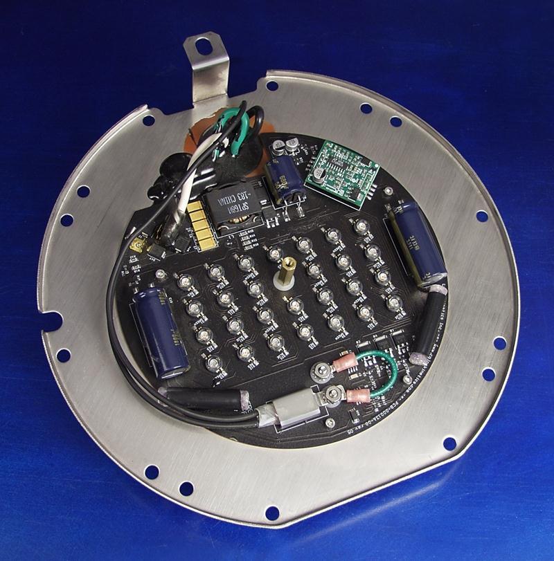
9 Specialized LED lighting applications
10
11 Optimizing the Insulated Metal Substrate application with proper material selection and circuit fabrication By Dave Sommervold Steve Taylor Chris Parker Garry Wexler
12 Introduction With the ever expanding growth in the use of insulated metal substrates (IMS ) used in high power density electronics and LED lighting designs, the complexity of the designs will require proper material selection and optimized circuit fabrication processes. The critical control of maximum junction temperatures require optimum thermal performance. The need to meet electrical isolation requirements is very important with most applications requiring safety agency testing, automotive is most exempt at this time, but still isolation is important, especially in inverter applications. Thus the importance of proper material selection, including type of base material, dielectric thermal performance and thickness, along with circuit foil weight must be thoroughly considered and defined.
13 Introduction The Design For Manufacturability (DFM) process must be utilized throughout the design, from the beginning circuit fabrication through final board assembly, to realize the optimum application performance. The PWB design and fabrication must also take into account how the final assembly process and the electrical testing requirements, including safety agency. Considerations for RoHS and REACH compliance must also be realized. Also all materials utilized must be compatible with today s Pb-free reflow assembly processes.

14 Material Selection Base Material Aluminum, Copper, Steel, AlSiC Dielectric Material Polymer/Ceramic- Blend Circuit Foil oz
15 Base Metals: Aluminum is bar far the most common in all applications: LED lighting, automotive power conversion and motor drives. Copper is found in high performance LED applications, semiconductor modules and specialty applications requiring a broad operating temperature range. The use of a copper base also deals with CTE mismatch issues when large ceramic packages are placed on an aluminum metal base. Also where maximum heat spreading is required to meet performance objectives. Dielectric: The key drivers Thermal Impedance, Dielectric Strength and Glass Transition Temperature (Tg).
16 Mechanical Considerations Flatness of the Finished Substrate CTE, Foil to Base Plate Thickness Ratio and Dielectric Tg Component / Solder Joint Stress Component Size, Component Material, Dielectric Tg and Base Material CTE Stiffness / Rigidity Base Material Dominated
17 IMS Flatness The flatness control is required due to the thermal expansion differences in the base material and the circuit foil from above Tg of the dielectric to ambient temperature during material manufacturing. Flatness can also be influenced after singulation with a forming process. Base materials with lower yield strength make forming less stressful on the finished circuit substrate.
18 Solder Joint Fatigue & Component Stress Solder Joint Fatigue can be reduced by choosing base materials with similar CTE and increased dielectric thickness. Smaller components will be under the least amount of strain. Dielectric with Tg in the operating temperature range of the application will allow for stress relief in the solder joints. High dielectric Storage Modulus will result in more stress on the solder joint.

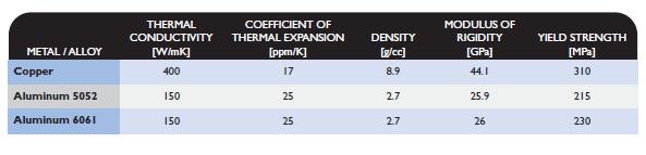
19 Selected Base Materials Properties
20 Thermal Considerations Thermal Impedance Dielectric thermal conductivity, thickness and interfacial resistances Heat Spreading Foil Weight, Base Thickness, Circuit Design Heat Generated due to I 2 R losses Foil Weight and applied current
21
22
23 Design Considerations for Singulation Methods Design Parameter Circuit to Edge Part Size Tolerance Flatness Tolerance Milling Scoring Blanking 1x material thickness depending on material thickness +/ / / / to / depending on material thickness* / to / depending on material thickness* 1x material thickness for aluminum, and 2x material thickness for copper / to / depending on material thickness* *Final part flatness (excluding scored arrays) can be influenced with a secondary forming process depending or ** during blanking on certain specific applications and base materials.
24 Electrical Considerations Application Voltage Safety Agency Test Voltages vs. Breakdown Voltages Permittivity Leakage Current Flashover Voltage Creepage Distance &Discharge
25 Safety Agency Test Voltages vs Breakdown Voltages Breakdown Voltages are NOT appropriate test voltages Typically testing at over 50% of breakdown strength damages the dielectric Recommended Proof Test voltages are specified by most suppliers

 - ENEPIG Au wire bondable NiPdAu plating (RoHS compliant) - Immersion Silver (RoHS compliant) - Tin (RoHS")
26 Laser Ablation -Ability to selectively remove dielectric in certain areas Multiple up Arrays -Allows for less handling during assembly Part Serialization and bar coding - white ink jet printer capable of smaller fonts than silk screening Surface finishes - Traditional HASL (not RoHS compliant) - Pb free HASL (RoHS compliant) - OSP (Organic Solder Preservative) - ENIG (RoHS compliant) - ENEPIG Au wire bondable NiPdAu plating (RoHS compliant) - Immersion Silver (RoHS compliant) - Tin (RoHS compliant)


27 T-Clad Standard V-Score V-scored parts tend to utilize the material most efficiently Eliminates the need for hard tooling required with a punched part Easy to separate from panel
28 Part Design For Scoring
29 Part Design Consideration for Piercing/Blanking -Minimum circuit to edge: 1x material thickness Minimum hole to edge: 1x material thickness -Minimum pierced hole size: 1.5x material thickness -Minimum annular ring: Minimum edge radius is one material thickness
30 Part Design For Blanking
31 Opportunities in Forming
32 Opportunities in Profiles
33
34 Special Processes
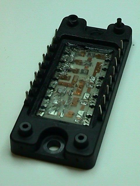
35 Applications
36
37
38
39

40 Conclusions IMS substrates provide many advantages and opportunities in power electronics designs with the variety of material selections and circuit fabrication possibilities. Can be greatly enhanced a strong technical relationship with the material and circuit fabricator. The amount of differentiation from traditional FR-4 forces the need apply design practices not previously considered.