SGS-Thomson L4990 Controller
|
|
|
- Angel Georgiana Austin
- 5 years ago
- Views:
Transcription
1 Construction Analysis SGS-Thomson L4990 Controller Report Number: SCA Global Semiconductor Industry the Serving Since N. Hartford Drive Scottsdale, AZ Phone: Fax: Internet:
2 INDEX TO TEXT TITLE PAGE INTRODUCTION 1 MAJOR FINDINGS 1 TECHNOLOGY DESCRIPTION Assembly 2 Die Process and Design 2-3 ANALYSIS RESULTS I Assembly 4-5 ANALYSIS RESULTS II Die Process and Design 6-8 TABLES Procedure 9 Overall Quality Evaluation 10 Package Markings 11 Wirebond Strength 11 Die Material Analysis 11 Horizontal Dimensions 12 Vertical Dimensions 13 i
3 INTRODUCTION This report describes a construction analysis of the SGS-Thomson L4990 controller. Five devices were supplied, encapsulated in 16-pin Dual-In-Line plastic packages (DIP). Devices were date coded MAJOR FINDINGS Questionable Items: 1 None. Special Features: BiCMOS with N+ buried layer, N-epi, P-wells in a P substrate. 1 These items present possible quality or reliability concerns. They should be discussed with the manufacturer to determine their possible impact on the intended application
4 TECHNOLOGY DESCRIPTION Assembly: Devices were encapsulated in 16-pin plastic Dip s. Lead-locking provisions (anchors and holes) were present at all pins. Thermosonic ball bond method employing 1.0 mil O.D. gold wire. Silver-filled epoxy die attach. Sawn dicing (full depth). Die Process and Design Fabrication process: Selective oxidation BiCMOS process employing N+ buried layer, N-epi in a P substrate. All devices were formed in N-epi with N+ buried layer. N-channel devices were formed in a P well within the N-epi and N+ buried layer. Final passivation: Three layers of passivation were employed. A layer of nitride over two layers of silicon-dioxide. The first layer of silicon-dioxide was very thin. Metallization: Two levels of silicon-doped aluminum defined by dry-etch techniques. No caps or barriers were employed. Standard contacts and vias (no plugs). Interlevel dielectric: Interlevel dielectric consisted of two layers of silicon-dioxide. The first layer appeared to have been subjected to an etchback. Pre-metal glass: A layer of reflow glass over densified oxides was used. Reflow was done prior to contact cuts
5 TECHNOLOGY DESCRIPTION (continued) Polysilicon: Single layer of dry-etched polysilicon (no silicide) was used to form all MOS gates on the die. Sidewall spacers were not employed. CMOS devices: Standard N+ and P+ implanted diffusions formed the sources/drains for these transistors. No LDD process was used. N-channel devices were located in P-wells within the N-epi/N+ buried layer. P-channel devices were located in the N-epi/N+ buried layer. Bipolar devices: Standard N+ diffusions (S/D) were used for emitters and collectors of NPN s and base contacts of PNP devices. Standard P+ diffusions (S/D) were also used on the PNP devices at the collector and emitter contacts for better ohmic contact. The base diffusions on the NPN device were a deep P+ diffusion (emitter and collector on PNP s). All bipolar devices were located in the N-epi and N+ buried layers. No buried contacts were employed. Isolation: Local oxide isolated MOS devices and P+ isolation diffusions (up and down) separated the N-epi islands
6 ANALYSIS RESULTS I Assembly: Figures 1-4 Note: Package analysis was not required. The following data was obtained by observation and is given here as general information. Questionable Items: 1 None. Special Features: Bond pads were oversized (6.3 x 6.3 mils) General Items: Devices were packages in 16-pin plastic Dip s. Package markings and date codes were clear and easy to read. Overall package quality: Normal. No defects were noted on the external portions of the package. Deflash was of normal quality and workmanship. Lead form was of normal quality and tinning was complete. No problems were found. Die placement: Die was centered on the header and silver-epoxy die attach was of good quantity and quality. No problems were found. Lead-locking provisions (anchors and holes) were present at all pins. 1 These items present possible quality or reliability concerns. They should be discussed with the manufacturer to determine their possible impact on the intended application
7 ANALYSIS RESULTS I (continued) Wirebonding: Thermosonic ball bond method using 1.0 mil O.D. gold wire. No bond lifts occurred and bond pull strengths were good (see page 9). Wire spacing and placement was good. Die dicing: Die separation was by full depth sawing with good quality workmanship
8 ANALYSIS RESULTS II Die Process and Design: Figures 5-26 Questionable Items: 1 None. Special Features: BiCMOS with N+ buried layer, N-epi, in a P substrate. General Items: Fabrication process: Selective oxidation BiCMOS process employing N+ buried layer, N-epi in a P substrate. All devices were formed in N-epi with N+ buried layer. N-channel devices were formed in a P well within the N-epi and N+ buried layer. Design and layout: Die layout was clean and efficient. No problems were noted. Die surface defects: None. No contamination or processing defects were noted. Final passivation: The passivation consisted of a layer of nitride over two layers of silicon-dioxide. The first layer glass was very thin. Passivation integrity test indicated defect free passivation. Edge seal was also good. Metallization: Two levels of metal defined by a dry-etch of normal quality. Metal 2 line profiles were somewhat unusual. The top portion of the line was wider than the main body of the metal. Metal consisted of silicon-doped aluminum. No cap or barrier metals were employed. Standard vias and contacts were used (no plugs). Contacts and vias were completely surrounded by metal. 1 These items present possible quality or reliability concerns. They should be discussed with the manufacturer to determine their possible impact on the intended application
9 ANALYSIS RESULTS II (continued) Metal defects: None. No voiding of the metal layers was present. Small notches were noted in the metal layers; however, no problems are foreseen. Small silicon nodules were noted following the removal of the metal, but no problems were present. Metal step coverage: Metal 2 aluminum thinned up to 70 percent at vias. Minimum metal 1 thinning was noted due to the slope etch of the contacts. MIL-STD-883D allows up to 70 percent metal thinning for contacts of this size. Contacts defects: None. Vias were steep and thick and no reflow was performed. The contact cuts were well sloped. No over-etching of the contacts were noted. No contact pitting or silicon mound growth was noted. Interlevel dielectric: Interlevel dielectric consisted of two layers of silicon-dioxide. The first layer appeared to have been subjected to an etchback. No problems were present. Pre-metal glass: A layer of reflow glass over densified oxides was used. Reflow was done prior to contact cuts. Polysilicon: Single layer of dry-etched polysilicon (no silicide) was used to form all MOS gates on the die. Sidewall spacers were not employed. No poly resistors were present. No problems were present. Local oxide (LOCOS) isolation. No step was noted in the oxide at the edge of the well. CMOS devices: Standard N+ and P+ implanted diffusions formed the sources/drains for these transistors. No LDD process was employed
10 ANALYSIS RESULTS II (continued) Bipolar devices: Standard N+ diffusions (S/D) were used for emitters and collectors of NPN s and base contacts of PNP devices. Standard P+ diffusions (S/D) were also used on the PNP devices at the collector and emitter contacts for better ohmic contact. The base diffusions on the NPN device were a deep P+ diffusion (emitter and collector on PNP s). All bipolar devices were located in the N-epi and N+ buried layers
11 PROCEDURE The devices were subjected to the following analysis procedures: External inspection X-ray Decapsulation Internal optical inspection SEM inspection of assembly features and passivation Wirepull test Passivation integrity test Passivation removal and inspect metal 2 Delayer to metal 1 and inspect Delayer to poly and inspect poly structures and die surface Die sectioning (90 for SEM) * Measure horizontal dimensions Measure vertical dimensions Material analysis * Delineation of cross-sections is by silicon etch unless otherwise indicated
12 OVERALL QUALITY EVALUATION: Overall Rating: Normal DETAIL OF EVALUATION Package integrity N Package markings G Die placement G Die attach quality G Wire spacing G Wirebond placement G (large bond pads) Wirebond quality G Dicing quality N Wirebond method Thermosonic ball bonds using 1.0 mil gold wire. Dicing method: Sawn (full depth) Die attach: Silver-filled epoxy Die surface integrity: Tool marks (absence): Particles (absence): Contamination (absence): Process defects (absence): General workmanship Passivation integrity Metal definition Metal integrity Contact coverage Contact registration Contact defects N N N N N G NP NP G N N G = Good, P = Poor, N = Normal, NP = Normal/Poor
13 PACKAGE MARKINGS Top (logo) L4990 N911A9531 MALAYSIA Bottom none WIREBOND STRENGTH Wire material: Die pad material: 1.0 mil diameter gold Aluminum Sample 1 # of wires tested: 10 Bond lifts: 0 Force to break - high: 15g - low: 12g - avg.: 13.9g - std. dev.: 1.0 DIE MATERIAL ANALYSIS Passivation: Die metallization: Interlevel dielectric: Pre-metal glass: Nitride over two layers of silicon-dioxide. Silicon-doped aluminum. Two layers of silicon dioxide. Layer of CVD glass over various densified oxides
14 HORIZONTAL DIMENSIONS Die size: 2.6 x 2.9 mm (102.5 x 114 mils) Die area: 7.5 mm 2 (11,685 mils 2 ) Min pad size: Min pad window: Min metal 2 width: Min metal 2 space: Min metal 2 pitch: Min via: Min metal 1 width: Min metal 1 space: Min metal 1 pitch: Min contact: Min poly width: Min poly space: 0.16 mm x 0.16 mm (6.3 x 6.3 mils) 0.15 mm x 0.15 mm (5.8 x 5.8 mils) 5.8 microns 6.4 microns 12.2 microns 4.0 microns 3.0 microns 3.0 microns 6.0 microns 1.8 microns 2.6 microns 3.2 microns Min gate length* - (N-channel) 2.6 microns - (P-channel) 4.0 microns PNP device Min P+ emitter: 7.5 microns NPN device Min N+ emitter: Min N+ emitter to edge of P+ base: 6.5 microns 2.5 microns P+ base to edge of isolation: 5.8 microns Min P+ isolation width: 11 microns * Physical gate length
15 VERTICAL DIMENSIONS Die thickness: 0.35 mm (14 mils) Layers Passivation 3: Passivation 2: Passivation 1: Aluminum 2: Interlevel dielectric-glass 2: -glass 1: Aluminum 1: Pre-metal glass: Poly: Local oxide: 0.9 micron 0.75 micron 0.2 micron 3.0 microns 0.6 micron micron 0.75 micron 0.6 micron 0.3 micron 1.0 micron N+ S/D diffusion - (NPN, N+ emitter and collector): 0.35 micron P+ S/D diffusion - (for ohmic contact at P+ contacts): 0.5 micron Deep P+: P well: 1.6 micron 5.0 microns N- epi: 6.0 microns N+ buried layer: 17 microns (from surface)
16 INDEX TO FIGURES PACKAGE ASSEMBLY Figures 1-4 DIE LAYOUT AND IDENTIFICATION Figures 5-7 PHYSICAL DIE STRUCTURES Figures 8-26 CROSS SECTION DRAWING Figure 21a BIPOLAR DEVICES Figures TYPICAL INPUT/OUTPUT CIRCUITRY Figure 26 ii

17 top SYNC 1 16 N.C. RCT 2 15 DC-LIM DC 3 14 DIS V REF 4 13 ISEN V FB COMP SGND PGND SS 7 10 OUT V CC 8 9 V C Figure 1. Package photograph and pinout of the SGS-Thomson L4990. Mag. 5x.


18 PIN 1 Figure 2. X-ray views of the package. Mag. 6.5x.


19 Mag. 200x EDGE OF PASSIVATION Mag. 1600x Figure 3. SEM views of dicing and edge seal. 60.


20 Au BOND PAD Au LEADFRAME Figure 4. SEM views of typical wirebonding. Mag. 625x, 60.

21 Figure 5. Whole die photograph of the SGS-Thomson L4990. Mag. 64x.


22 Mag. 200x Mag. 320x Figure 6. Optical photographs of markings on the die surface.


23 Figure 7. Optical views of the die corners. Mag. 160x.


24 Mag. 1400x Mag. 3200x Figure 8. Perspective SEM views of overlay passivation coverage. 60.


25 PASSIVATION METAL 2 POLY GATE glass etch, Mag. 3200x PASSIVATION 2 PASSIVATION 3 N+ S/D POLY Mag. 6500x Figure 9. SEM section views of general structure.


26 PASSIVATION METAL 2 Mag. 3200x PASSIVATION 3 PASSIVATION 2 PASSIVATION 1 METAL 2 Mag. 10,000x Figure 10. SEM section views of metal 2 line profiles.


27 VIA METAL 2 Mag. 810x NOTCHES VIA METAL 2 Mag. 1600x Figure 11. Topological SEM views of metal 2 patterning. 0.


28 VIA METAL 2 Mag. 1600x, 60 METAL 2 VIA Mag. 5000x, 60 PASSIVATION 70% THINNING METAL 2 Mag. 6500x Figure 12. SEM views of metal w2 coverage and M2-to-M1 via.


29 METAL 2 POLY Mag. 6500x Si Si INTERLEVEL DIELECTRIC PRE-METAL DIELECTRIC Mag. 13,000x Figure 13. SEM section views of metal 1 line profiles.


30 VIA CONTACT Mag. 1100x POLY CONTACT Mag. 2200x Figure 14. Topological SEM views of metal 1 patterning. 0.


31 METAL 2 VIA CONTACT Mag. 1400x POLY Mag. 10,000x Figure 15. SEM views of metal 1 coverage. 60.


32 metal 1-to-poly POLY LOCAL OXIDE PASSIVATION INTERLEVEL DIELECTRIC metal 1-to-N+ N+ DIFFUSION PASSIVATION metal 1-to-P+ INTERLEVEL DIELECTRIC P+ DIFFUSION Figure 16. SEM section views of metal 1 contacts. Mag. 13,000x.


33 POLY Mag. 440x DIFFUSION POLY GATES POLY Mag. 775x Figure 17. Topological SEM views of poly patterning. 0.


34 POLY Mag. 1600x GATES POLY Mag. 13,000x DIFFUSION POLY Mag. 13,000x DIFFUSION Figure 18. Perspective SEM views of poly coverage. 60.


35 PRE-METAL DIELECTRIC POLY N+ S/D N+ S/D GATE OXIDE N-channel PRE-METAL DIELECTRIC POLY P+ S/D P+ S/D GATE OXIDE P-channel Figure 19. SEM section views of typical transistors. Mag. 13,000x.

36 OXIDE ON POLY POLY LOCAL OXIDE GATE OXIDE Figure 20. SEM section view of a local oxide birdsbeak. Mag. 26,000x. N-EPI N+ BURIED LAYER P-channel N-channel P-WELL N+ BURIED LAYER Figure 21. Optical section views of the well structure. Mag. 800x.
37 PASSIVATION 1 SGS-Thomson L4990 PASSIVATION 3 PASSIVATION 2 METAL 2 INTERLEVEL DIELECTRIC,,,,,,,,,,,,,,,,,, P-WELL N-EPI LOCAL OXIDE PRE-METAL DIELECTRIC POLY N+ S/D P+ S/D N+ BURIED LAYER P+ ISO P SUBSTRATE N-EPI Orange = Nitride, Blue = Metal, Yellow = Oxide, Green = Poly, Red = Diffusion, and Gray = Substrate Figure 21a. Color cross section drawing illustrating device structure. N+ BURIED LAYER


38 COLLECTOR BASE EMITTER intact BASE COLLECTOR delayered EMITTER N-EPI N+ BURIED LAYER P+ EMITTER P+ COLLECTOR Figure 22. Optical views of the PNP device. Mag. 800x.


39 METAL 2 Mag. 1600x N-EPI N+ BURIED LAYER P+ EMITTER CONTACT P+ COLLECTOR CONTACT INTERLEVEL DIELECTRIC emitter, Mag. 13,000x P+ EMITTER CONTACT INTERLEVEL DIELECTRIC collector, Mag. 13,000x P+ COLLECTOR CONTACT Figure 23. SEM section views of the PNP device.


40 intact N+ EMITTER P+ BASE N+ COLLECTOR delayered P+ BASE N+ BURIED LAYER N-EPI Figure 24. Optical views of the NPN device. Mag. 800x.


41 METAL 2 Mag. 1600x P+ BASE N+ COLLECTOR base contact, Mag. 6500x P+ BASE P+ collector contact, Mag. 6500x N+ COLLECTOR Figure 25. SEM section views of the NPN device.


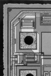
42 Mag. 400x Mag. 200x Figure 26. Optical views of general circuitry and I/O structure.