# of credit hours = 3 EEE Course prerequisites, corequisites, and where the course fits in the program of study
|
|
|
- Junior Jordan
- 5 years ago
- Views:
Transcription
1
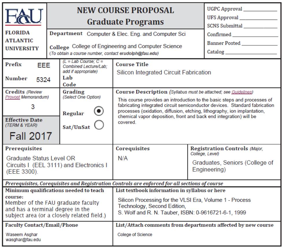
2 Department of Computer & Electrical Engineering 1. Course title/number, number of credit hours Silicon Integrated Circuit Fabrication # of credit hours = 3 EEE Course prerequisites, corequisites, and where the course fits in the program of study Prerequisites: Graduate Status Level OR Circuits I (EEL 3111) and Electronics I (EEE 3300). 3. Course logistics Term: Location: TBD 4. Instructor contact information Instructor s name Office address Office Hours Contact telephone number address 5. TA contact information TA s name Office address Office Hours Contact telephone number address 6. Course description Bldg. EE 96/ Room 435 TBD wasghar@fau.edu TBD This course provides an introduction to the basic steps and processes of fabricating integrated circuit semiconductor devices. Standard fabrication processes (oxidation, diffusion, etching, lithography, ion implantation, chemical vapor deposition, front and back end integration) will be covered. Concepts and processes related to BioMEMS and microfluidics will also be explained. 7. Course objectives/student learning outcomes/program outcomes Course objectives To introduce the students to the concepts of silicon integrated circuit fabrication processes and modules. 8. Course evaluation method 5 Homework assignments (4% each) : 20% Term paper: 20% Midterm exam: 20% Final exam: 40% For term paper, students will be divided into group of 2 3 students. Each group will propose an interesting topic related to latest key advances in the field of Silicon Integrated Circuit Fabrication. Each group will present their proposal topic in class and also submit a comprehensive report on the proposed topic.
3 9. Course grading scale Department of Computer & Electrical Engineering Grading Scale: 90 and above: A, 87 89: A, 83 86: B+, 80 82: B, : B, 73 76: C+, 70 72: C, 67 69: C, 63 66: D+, 60 62: D, 51 59: D, 50 and below: F. 10. Policy on makeup tests, late work, and incompletes Students are strongly suggested to inform the instructor in advance in the case of emergency (if possible). Makeup exams are given only if there is solid evidence of a medical or otherwise serious emergency that prevents the student of participating in the exam. Students must turn in homework, assignment and projects on time. Students may lose 25% (after 1 day) and 50% of marks (after 2 days) if they turn in late. Submissions may not accepted after 2 nd day of due date. 11. Special course requirements 12. Classroom etiquette policy University policy requires that in order to enhance and maintain a productive atmosphere for education, personal communication devices, such as cellular phones and laptops, are to be disabled in class sessions. 13. Disability policy statement In compliance with the Americans with Disabilities Act Amendments Act (ADAAA), students who require reasonable accommodations due to a disability to properly execute coursework must register with Student Accessibility Services (SAS) in Boca Raton, SU 133 ( ); in Davie, LA 131 ( ); or in Jupiter, SR 111F ( ) and follow all SAS procedures. 14. Honor code policy Students at are expected to maintain the highest ethical standards. Academic dishonesty is considered a serious breach of these ethical standards, because it interferes with the university mission to provide a high quality education in which no student enjoys unfair advantage over any other. Academic dishonesty is also destructive of the university community, which is grounded in a system of mutual trust and place high value on personal integrity and individual responsibility. Harsh penalties are associated with academic dishonesty. See University Regulation at Required texts/reading Silicon Processing for the VLSI Era, Volume 1 Process Technology, Second Edition, S. Wolf and R. N. Tauber, ISBN: , Supplementary/recommended readings Research papers will be given at the end of lectures to read and understand. 1. Lee et al. Ge GAA FETs and TMD FinFETs for the Applications Beyond Si A Review, IEEE
4 Department of Computer & Electrical Engineering Journal of the Electron Devices Society ( Volume: 4, Issue: 5, Sept ). 2. Tans et al. Room temperature transistor based on a single carbon nanotube, Nature 393, (7 May 1998) 3. Das et al. Mechanisms of material removal and mass transport in focused ion beam nanopore formation, Journal of Applied Physics, Volume 117, Issue 8, Feynman, There's plenty of room at the bottom, the annual meeting of the American Physical Society (APS) at the California Institute of Technology, Kim et al., Silicon Based BioFETs with 3 D Nanostructure: Easy integration, precise control of nanostructure, and a low device to device variation, IEEE Nanotechnology Magazine ( Volume: 10, Issue: 3, Sept ) 6. Mariana et al., An Inkjet Printed Field Effect Transistor for Label Free Biosensing, Advanced Functional Materials, Vacic et al., Calibration methods for silicon nanowire BioFETs, International Conference on Microelectronic Test Structures (ICMTS), Ye at al., Atomic layer deposition of ZrO2 as gate dielectrics for AlGaN/GaN metal insulatorsemiconductor high electron mobility transistors on silicon, Applied Physics Letters, Volume 103, Issue 14, Course topical outline, including dates for exams/quizzes, papers, completion of reading Weekly Schedule Topics Week 01 Week 02 Week 03 IC Process Overview & Wafer Fabrication: Historical perspective a sampling of key inventions and discoveries, Design to package workflow Fab process types, crystal structure basics, physical properties Crystal Defects: Monovacancy, Divacancy, Microvoids, Voids, Antisites, Interstitials, Dislocation, Stacking fault, Grain Boundaries, Precipitates. Wafer Fabrication: Czochralski (CZ), Float Zone (FZ), Molecular Beam Epitaxy Thermal Oxidation: Oxidation kinetics (general solution, Parabolic and linear growth and empirical modifications to the growth rate of SiO2 and its kinetics), Thermal Nitridation Factors in oxidation, Applications of oxide and nitride layers in IC fabrication, SiO2/Si interface, charge traps and impurities redistribution at the interface, Oxidation systems, Measurement techniques HW 1 Week 04 Diffusion: Fick's first and second law and their solutions, Mechanism of diffusion, Profile and Junction Depth and techniques of their determination Effect of electric field on diffusion process Impurity diffusion in IC fabrication (Boron, Phosphorus, Ar). Diffusion Systems [equipment, sources (gas, liquid, solid)] Measurement techniques. HW 2
5 Week 05 Department of Computer & Electrical Engineering Lithography 1 Photoresists (positive and negative) Resist chemistry (Photo sensitive and base) Physical properties (Sensitivity, Photo Speed, Resolution, etc.) Resists and Process: Photolithography steps (Coat, Soft bake, Patterning and Exposure, Post Exposure Bake, Develop, Inspection) Coat and Coaters (Thickness control, uniformity, etc.), Soft Bake and its effects on the film properties and consequent steps Week 06 Lithography 2: Patterning and exposure, Criteria, limits, resist dependency, equipment, alignment, etc.) Bosung Curves, Focus exposure matrix, Post Exposure Bake, and its effects on the pattern, Develop (batch, spray, and puddle). Week 07 Week 08 HW 3 Developer chemistry, development time, Critical Dimensions (CD) and Inspection (pattern integrity, notching, bridging, etc.) Midterm Exam Etch and Cleans: Introduction to dry etch, Etch output parameters, Process monitoring (OES and EPD), Etch Equipment Cleans: Intro to contamination types, sources, and impact, Wafer cleaning, Particle removal, Defect detection For term paper proposal, students will be divided into group of 2 3 students. Each group will propose an interesting topic related to latest key advances in the filed of Silicon Integrated Circuit Fabrication. Each group will present their proposal topic in class and also submit a comprehensive report on the proposed topic. Week 09 Term Paper Proposal Chemical Vapor Deposition: Introduction to Chemical Vapor Deposition (CVD), Basics, Grove s simplified growth model, Gas flow CVD Systems Systems, Reactors, MFCs, PECVD, Example films deposited by CVD: Polysilicon, SiO2, Silicon Nitride, Tungsten Week 10 Week 11 HW 4 Epitaxy: Epitaxy: Intro and Applications, Growth, Defects, Low Temperature Growth Selective Epitaxy, Strained Silicon, Equipment, Characterization Physical Vapor Deposition: Thermal Evaporation, E beam Evaporation, SOI Wafers Sputtering Process: Sputtering deposition and Equipment, Applications of Sputtering, glow discharge, RF sputter, magnetron sputter, mechanism, deposition rate, advantages and disadvantages, etc.), Contacts and Vias, Morphology and Step Coverage, Aspect Ratio
6 Department of Computer & Electrical Engineering HW 5 Week 12 Week 13 Week 14 Week 15 Ion Implantation: Dose, Beam Current, Range and Projected Range Projected and Lateral Straggle, Ion Stopping (nuclear and electronic energy loss mechanism), Implantation in amorphous and single crystal (channeling effect) Ion implantation damage, Electrical activation and implantation damage recovery (Annealing and RTP), Ion Implantation equipment, Masking layers, Shallow Junction, Measurement techniques Back End Integration: Introduction & Conventional Flow, Propagation Delay, Choice of Materials Metal Deposition and Via Filling, Aluminum, Tungsten, Copper, Low k Dielectrics, Damascene Integration Planarization and Passivation: BPSG Reflow, Etch Back, Deposition Etch Cycles, Spin on Glass, Choice of Deposition Chemical Mechanical Polishing: Intro to CMP, Local and Global Planarization, Dummy Features, CMP Removal Rates, Slurry Types, Pad Types, Slurry, CMP Defects. Front End Integration: Introduction and History, 0.5μm to 1.2μm Process Flow (circa 1990), Wells and Channel stop, LOCOS isolation, Vt adjust and Gate formation, Source/Drains, PMD and Contacts Deep sub Micron (<0.25 μm) Process Flow (circa 2000), Shallow Trench, Isolation, Retrograde Wells and Vt adjust, Gate formation, Source/Drains with extensions (tips), Salicide, PMD and Contacts Term Paper Presentation and Report Submission Final Exam
7 From: Charles Roberts Sent: Wednesday, February 15, :10 AM To: Mihaela Cardei Cc: Waseem Asghar Subject: Re: Request of Approval Silicon Integrated Circuit Fabrication To: UGPC Subject: EEE 5324 Integrated Circuit Fabrication Date: 2/15/2017 The College of Science supports the College of Engineering in offering this course, NCP EEE5324, and recommends approval by the Faculty Senate. Charles Roberts Chair, Charles E. Schmidt College of Science Curriculum Committee Associate Dean of Graduate Studies Charles E. Schmidt College of Science From: Mihaela Cardei Sent: Wednesday, February 15, :51:26 AM To: Charles Roberts Cc: Mihaela Cardei; Waseem Asghar Subject: Request of Approval Silicon Integrated Circuit Fabrication Dear Dr. Roberts, The Department of Computer and Electrical Engineering (CEECS) is proposing a new course EEE 5324 Silicon Integrated Circuit Fabrication. Please find attached the course proposal. This course was discussed in the UGPC yesterday on February 14th, and it was suggested to get a support letter from the College of Science. Could you please review the proposal and me your approval decision? Thank you, Mihaela Mihaela Cardei, PhD Professor and Director Graduate Studies Computer & Electrical Engineering Department College of Engineering, FAU