Nanoindentation-induced Mechanical Responses
|
|
|
- Della Burns
- 5 years ago
- Views:
Transcription
1 Chapter 3 Nanoindentation-induced Mechanical Responses The technological drive for introducing nanoscopic devices is faced with the breakdown of continuum theories and traditional scaling approaches. In this mesoscopic regime, material characteristics become dominated by interfacial and dimensional constraints. Progress in this direction strongly depends on the development of appropriate techniques used to analyze surface and structural properties on the micro/nanometer-scales. Over the past two decades, several contact mechanical approaches have been developed to meet these needs; e.g., the Scanning Probe Microscopes (SPMs) and Depth-sensing Indentation (DSI). As nanoindentation becomes a standard engineering tool, it is useful to establish a connection between the atomic scale processes during the indentation and the 61
2 measurable mechanical characterizations. The usual mechanical properties that are determined during nanoindentation are Young s modulus and the hardness of the materials. The method has many potential applications for examining nanoscale mechanical characterizations of small areas and thin films. Experimentally, we present a systematic study of the mechanical properties of the semiconductors by means of in-situ and ex-situ techniques to characterize the mechanical deformation behaviors. Characteristic techniques used include: Nanoindenter, Atomic Force Microscope (AFM), micro-raman Spectroscopy, Scanning Electron Microscope (SEM), Focused-ion Beam (FIB) and Transmission Electron Microscope (TEM) techniques to reveal the mechanical deformation mechanisms of Group IV (Si and Ge) and Group III-V (GaAs, GaN, GaSb and InP) semiconductors. Results revealed that in both Si and Ge there was a transformed zone immediately under the indent composed of amorphous and mixture phases. Nevertheless, for Group III-V semiconductors, the mechanical deformation was shown proceed solely by the formation and propagation of dislocations, and not phase transformation. The mechanical properties of III-V semiconductors such as GaAs are very important to optoelectronic applications as they determine the structural quality of the heterostructures and therefore the performance of the devices. Herein, complementary experiments and Molecular Dynamics (MD) simulations have 62
3 been carried out to determine the atomistic mechanisms of semiconductors during contact evolution. MD simulations based on the Tersoff s potential to simulate interatomic forces between the sample and the tip is performed to study the evolution of the deformed region during nanoindentation processes. MD simulations indicates that the semiconductors deform plastically at various effects of loads and temperatures and, our results are able to give a good description even for an ultra-small penetration depth (<3nm). The load-displacement curves are used to derive the hardness and Young s modulus of the semiconductors by using a Berkovich pyramid-shaped indenter. There is also qualitatively agreement between the experimental and theoretical load-displacement curves. MD results and the experimental observations present the mechanism and the occurring processes during nanoindentation, which supports many of the experimental features. In this chapter, details of nanoindentation-induced mechanical deformation of GaAs have been investigated. Parts of this chapter have been published in: 1.) S.R. Jian, T.H. Fang and D.S. Chuu, J. Electron. Mater. 32 (2003) 496; 2.) S.R. Jian, T.H. Fang and D.S. Chuu, Appl. Surf. Sci. 252 (2006) 3033; 3.) S.R. Jian, T.H. Fang and D.S. Chuu, Appl. Surf. Sci. (2006, in press). 63
4 3.1 Background information The physical properties of materials can be investigated under static pressures of millions of atmospheres and temperatures of several thousand Kelvin because of the advent of the Diamond Anvil Cell (DAC) technique. Study of materials over such a large pressure and temperature range has resulted in the identification of new structures and has provided a fundamental understanding of physical transformations that take place under extreme conditions [1-2]. In some cases, the high pressure and/or high temperature phase of interest can be quenched to ambient conditions, allowing further ex-situ characterization. Of particular interest is study of mechanical properties, such as hardness and the quenched phase [3]. Nevertheless, this type of measurement has been impractical because of the very small sample volumes required in DAC devices where the sample chamber is typically only µm in diameter, depending on the maximum pressure needed. Nowadays, the difficulty has overcome by taking advantage of the small probe volume available from a depth-sensing nanoindenter. In many aspects of technology, there is a drive for smaller and smaller components. With decreasing the volume of materials, the response of materials to characterization techniques may be different from their bulk form. One explanation for the change in behavior is the increased role of the surface. The mechanical properties of the near-surface region of a component often determine its service life in tribological applications. In particular, there is considerable interest in determining the mechanical characterizations of semiconductors. Indeed, studies of the processes controlling contact damage, wear and cracking of semiconductor materials have significantly technological importance. Nevertheless, accurate determination of the mechanical properties of semiconductors requires a thorough understanding of the 64
5 physical processes occurring during deformation. Depth-sensing indentation or Nanoindentation has become a popular tool of quantitative small-volume mechanical characterizations determination of the various materials have dramatically advanced our understanding of the transition between elastic and plastic deformation at the nanometer-scale. In most nanoindentation systems a load is continuously applied to an indenter tip and the penetration depth of an indenter tip into the sample is measured as a function of indentation load. From the unloading slope of the load-displacement curve the contact stiffness, contact area, and mechanical properties such as hardness and Young s modulus of materials can be calculated using well-established models [4]. Due to its high spatial resolution in all three dimensions, nanoindentation is compatible with investigating the local mechanical characterizations of thin films, composites and engineered surface, as well as the structural mechanics of micro-electro-mechanical systems and other miniature devices. Although the scale of measurement presents its unique set of challenges, nanoindentation is conceptually a simple technique: force, displacement and time are recorded continuously while a well-defined indentation probe, usually diamond shaped as trigonal pyramid, is pushed into a test sample in a controlled manner. Indentation hardness is determined by analyzing the unloading segment of load-displacement curve (Fig.3-1) taking advantage of the Oliver-Pharr method [5] regardless of the choice of indenter geometry. However, nanoindentation is slightly different than macroscale hardness tests and requires a number of significant assumptions. In some environments these assumptions can lead to significant sources of error. This section presents an introduction into this testing technique, including a presentation of the testing machine and a review of the analysis method used in this work. In addition, in order to understand why our records might be inaccurate, some of the common material 65
6 aspects that need to be corrected for are discussed in the following sections. The contact area is a crucial parameter in hardness testing, and it is assumed based upon the displacement of the indenter tip. If the surface is not ideally flat, the actual contact area can differ significantly from the predicted value. The contact area can be charged by pile-up and/or sink-in around the indenter, and surface roughness of materials. All of these contact area changes are discussed in 3.1-2, and the time dependent influences on mechanical characterizations are also presented. Nanoindentation imposes a complex stress field, but over these years, much has been learned towards correlating its results to classical forms of mechanical characterizations testing. In addition to indentation hardness, quantities such as elastic modulus, yield stress, strain-rate sensitivity and fracture toughness can be extracted from nanoindentation tests. While nanoindentation often agrees with larger-scale techniques, there are certain environments in which the mechanical behaviors at nanometer-scale are definitely different. For metals, the details of indentation-induced incipient plasticity in test volumes small enough to avoid pre-existing dislocations is of considerable fundamental interest to both experiments [6] and theoretical studies [7] have recently been attracting much attention. In this limit, the critical shear stress at the onset of plasticity is governed by the requirements for dislocation nucleation rather than by the energy barrier to dislocation motion. The scale of the experiments is the cause of much of the inherent complexity of the measurements, for the tests are on the order of material features such as dislocations. The mechanical behaviors of small volume of materials are not well understood. We have theories about an idealistic atomic-scale and have simplified models to explain the materials behaviors. Nanoindentation tests are small enough that there may be influences that would be masked on a larger scale. It is more complex than an idealized atom sized mechanism. Monitoring of the displacement in a material as an indentation load is applied 66
7 describes a great deal about the surface, the stress state and defects/or dislocations presence. Understanding the contribution of surface and the nanoindentation-induced plastic deformation behaviors on mechanical response can eventually enable suiting of material for specific properties requirements. An excellent practical guide devoted entirely to the nanoindentation technique is the recently published book by Fischer-Cripps titled Nanoindentation [4]. This book addresses both strengths and limitations of the technique, and devoted an entire chapter to descriptions and specifications of commercially available nanoindentation equipment. Also, perhaps the most read treatise on the fundamentals of contact mechanics is the classic book by Johnson titled Contact Mechanics [8], which thoroughly addresses the Hertz s theory that is sometimes used to analyze the loading segment of load-displacement curves obtained with the various indentation probes Nanoindentation analysis Recently developments in nanotechnology have realized the miniaturization of materials, such as the production of micro/nano-electromechanical systems. The miniaturization of structures demands the establishment of a technique that evaluates the mechanical properties of micro/nano-structured materials. In order to measure the mechanical properties of these materials, indentation hardness test equipment must have high spatial (in the nanometer-scale range) and load (in the nn range) resolution. The Nanoindenter is one tool that can measure the local mechanical properties of micro/nano-structured materials. A nanoindentation measurement is accomplished by pushing a small three-sided Berkovich-shaped diamond indenter into a sample and then withdrawing it, recording 67
8 the force required as a function of position. A typical load-displacement curve obtained from In 0.25 Ga 0.75 N thin film is displayed in Fig.3-1, here h max represents the maximum penetration depth of the indenter corresponding to the maximum indentation load applied, P max, during the indentation and h f is the residual depth after removing the indenter. The contact depth h c is the intercept of the tangent line drawn from the first part of the unloading curve, which described the elastic deformation effects [5]. The slope of the upper potion of the unloading curve during the initial stages of unloading, S, also called the contact stiffness. The accuracy of hardness and modulus measurement depends inherently on how well these parameters can be measured experimentally. The analysis used to determine the hardness, H, and elastic modulus, E, is essentially an extension of the method proposed by Doerner and Nix [9] that accounts for the fact that unloading curves are distinctly curved in a manner that cannot be accounted for by the flat punch approximation. Using the approximation [9] in the flat punch, the contact area remains constant as the indenter is withdrawn, and the resulting unloading curve is linear. In contrast, experiments have shown that unloading curves are distinctly curved and usually well approximated by the power law relation: ( h ) m P = α (3.1.1) h f where α and m are power law fitting constants [5]. The variation of the power law exponents in the range 1.2 m 1. 6 demonstrates not only that the flat punch approximation is inadequate ( m = 1 for the flat punch), but also that the indenter appears to behave more like a paraboloid of revolution, for which m =1. 5 [10]. This result was somewhat surprising because the axisymmetric equivalent of the Berkovich indenter is a cone, for which m = 2. This discrepancy has since been explained by the 68
9 concept of an effective indenter shape [11]. The exact procedure used to measure H and E is based on the unloading processes shown schematically in Fig.3-2, where it is assumed that the behavior of the Berkovich indenter can be modeled by a conical indenter with a half-included angle, φ, that gives the same depth-to area relationship, φ = The basic assumption is that the contact periphery sink-in in a manner that can be described by models for indentation of a flat elastic half-space by rigid punches of simple geometry [9]. This assumption limits the applicability of the method because it does not account for the pile-up of material at the contact periphery that occurs in some elastic-plastic materials. Assuming, however, that pile-up is negligible, the elastic models show that the amount of sink-in, h s, is given by: h s Pmax = ε (3.1.2) S where ε is a constant that depends on the geometry of the indenter. Important values are: ε = 0.72 for a conical punch, ε = 0.75 for a paraboloid of revolution (which approximates to a sphere at small depths), and ε = 1.00 for a flat punch [10]. Using Eq.(3.1.2) to approximate the vertical displacement of the contact periphery, it follows from the geometry of Fig.3-2 that the depth along which contact is made between the indenter and the sample, h c = h max h, is: s h c Pmax = hmax ε, (3.1.3) S here ε = 0.75 is a geometrical constant associated with the shape of a Berkovich indenter [5]. S = dp / dh, is the unloading stiffness can be derived from the slope of the initial portion of the unloading curve. This method of determining the contact depth is commonly referred to as the Oliver-Pharr method [5]. Once h c is determined, the projected area A c of actual contact can then be calculated using the cross-sectional shape of the indenter along its 69
10 length. The area function f ( ) A = calculated for the Berkovich tip, can be the c h c expressed as a function of the form: 2 c 1 1/ 2 2hc 1/ 4 3hc A c = 24.56h + C hc + C + C + C hc, (3.1.4) 4 1/8 where the parameters C 1 = , 4 C 2 = , 5 C 3 = and 5 C 4 = For example, in Hysitron system, these parameters of above equation can then be inputted into the Data Analysis section of the TriboScope Nanoindenter for use on any further indenters made at depths in the calibration range. Our operate procedures as follow above-mentioned, so our experimental data is well accepted. The analysis software is used by the TriboScope 3.5 Software Package which contains the capabilities for the automatic calculation of nanomechanical properties, automated correction for tip calibration and so on. In depth-sensing measurements, it is essential to ascertain the detailed procedures and further discussion of the mechanism on nanometer-scale. Based on the recorded of the previously studies and the standard operate procedures of TriboScope Nanoindenter; our investigation is very powerful and suitable for recognizing the properties of films. Hardness of a material is defined as its resistance to local plastic deformation. Once the contact area is determined, hardness H is determined from maximum indentation load P max divided by actual projected area of contact as P H =, (3.1.5) max A c The other material property often sought in indentation testing is the modulus of the material. There is one major assumption in the calculation of the indentation modulus: that it remains constant over all depths. The reduced modulus is calculated using the contact area and the stiffness: 70
11 E r 1 π = S, (3.1.6) 2β A c where β is a shape constant of for the Berkovich tip. E r is the reduced elastic modulus which accounts for the face that elastic deformation occurs in both the sample and indenter, is defined as v 1 f vi E = + r, (3.1.7) E f Ei where E and v with subscripts f and i are the Young s modulus and Poisson s ratios of the material and the indenter, respectively. For a diamond indenter tip, E i =1140GPa and v i =0.07 [5] Potential sources of data distortion In the previous section, we have described the indentation-induced plastic behavior and the analysis methods used to calculate materials mechanical properties from the penetration depth that occurs as a load is applied. During the nanoindentation process, there are other sources of error for tests that are caused by the materials and the testing parameters. Unlike those associated with that apparatus, these distortions are materials specific and therefore harder to identify and correct. Accurate knowledge of the contact area is important in determining a truly representative hardness value. Some materials exhibit deformation behavior that can lead to significant miscalculations in the contact area. Under the loading, some materials pile-up surrounds the indenter increasing the contact area. Other materials experience sink-in, seeming to collapse from the area surrounding the indenter. There are other contact area problems which are introduced because of the scale of testing. 71
12 Surface irregulars and roughness are not significant issues at the macroscale but can influence nanoindentation considerably. Identification of behavior that might alter contact area will help us determine the accuracy of measured hardness values. Certain materials exhibit time dependent deformation. Creep is defined as continued plasticity at a constant load. The continued deformation is often apparent in the hold at maximum load. The rate at which the probe comes in contact with materials can also have a significant influence on the indentation behavior. Materials that demonstrate displacement bursts at the onset of plasticity have shown this property to be time dependent. In the materials that are subjected to time dependent plasticity, the measured mechanical properties may vary depending upon the testing parameters. Identifying when a material is affected by the duration and rate of contact may help us to adjust testing parameters to achieve more repeatable results. Further details of the property of time dependent plasticity due to nanoindentation can be found elsewhere [12-13]. Contact Area Changes One of the most significant attributes of nanoindentation is that analysis of the residual deformation is not directly measured to determine the mechanical properties of materials. This method relies on calculated contacts based on idealized materials behavior. Anything that distorts that contact area makes the mechanical properties inaccurate. In this section, we address some of the potential sources for inaccurate estimation of contact area. a.) Pile-up and Sink-in At a particular depth of penetration the contact area is dependent not only upon the tip shape, but also the elastic properties of materials. Fig.3-3 is a schematic of two 72
13 situations shown in cross section and a top view. The left-hand side of this figure illustrates sink-in even, or a reduction in contact area, while the right-hand side illustrates pile-up even that can significantly increase the contact area. These figures demonstrate that the extent of elastic deformation can dramatically change the contact area from that predicted by the total displacement of the tip. The Oliver-Pharr method makes the reasonable mechanical properties for most materials. Since the analysis technique is based on an idealized elastic contact, which predicts materials to be drawn downward during contact, the Olive-Pharr method is a good method for materials that experience sink-in. The influence of pile-up is more pronounced on property calculations. As reported by Bolshakov and Pharr [14], all materials with a ratio of h f / h max below 0.7 exhibits sink-in even; while the materials with a ratio of h f / h max above 0.7 shows pile-up even. In the case of sink-in event, the shape of the indentation revealed that the sides of the indentation recover more than the corners. This is probably due to the difference in stress concentration induced in the material during nanoindentation. The stress concentration is greater at the corners of a Berkovich tip than its sides. On the other hand, it is a common misunderstanding that soft metals experience significant pile-up all of the time. The problem of pile-up is often extreme in situation of a soft film on a hard substrate, for the indents often penetrate well into the substrate [15]. When additional plasticity occurs near the indenter, pile-up occurs; i.e. the change in yield strength means that the material at the edge of the plastic zone is soft than that directly under the tip. The effects of pile-up/sink-in on the hardness and Young s modulus can be neglected due to the fact that Young s modulus remains essentially constant over the indentation penetration depth. 73
14 b.) Surface Roughness The elastic contact model used for evaluation of the load-displacement curves is based on the assumption of a single contact between the indenter tip and a homogeneous, perfectly elastic material having a smooth surface. If the surface is rough, multiple area contacts between an indenter tip and asperities of the surface are formed instead of a single contact, please see in Fig.3-4(a). Because the contact area of a single asperity-tip contact is small, the stress in this area is high even at a small load. Consequently, the asperity deforms plastically at a very early stage of the indentation experiment, i.e. at a low loading, causing the load-displacement curve to cover larger displacements than in the case of a sample with a smooth surface, please see Fig.3-4(b) [16]. As a result, the projected contact area is overestimated and the values for hardness and indentation modulus calculated from Eqs.( ), respectively, are too small [17]. To counteract influence owing to the surface roughness, the indentation depth must be large relative to the roughness. Analysis of the surface roughness is usually performed by SPM. For the quantification of surface roughness, several parameters have been applied in Ref.18. Most commonly, height parameters as the roughness average or the root-mean-square (RMS) are utilized. The RMS roughness is used as defined [19] 1/ 2 2 n 1 RMS = ( y i y), (3.1.8) n i= 1 where n is the number of data points in the profile, y i are the data points that describe the relative vertical height of the surface and, y is the mean height of the surface. The latter is given by 1 y = n n y i i= 1, (3.1.9) Bobji et al. [20] found that the roughness manifestly increases the scatter of 74
15 hardness, especially at small penetration depths by finite element analysis. The material was measured to be significantly harder at smaller penetration depth. Zhang and Xu [21] investigated the surface effect on nanoindentation and introduced an apparent surface stress that represents the energy dissipated per unit area of a solid surface in a nanoindentation measurement. They considered the work done by an applied indentation load that contains both bulk and surface stress. This surface work, which is related to the apparent surface stress and the indenter tip parameters, is necessary in the deformation of a solid surface. As reported in Ref.12, we proposed that the variation in the depth-dependent hardness with various indium contents in In x Ga 1-x N thin films may be caused by the anisotropic behavior of the apparent surface stress. The rougher the surface, the higher the surface stress is. The rougher surface may consume more energy during nanoindentation and thus leads to a higher apparent surface stress. Time Dependent Properties a.) Creep Nanoindentation assumes elastic-to-plastic behavior and can not take into account any time dependent plasticity behavior, i.e. creep, which is often observed in indentation testing as continued deformation during the hold at maximum indentation load. Creep is indistinguishable from thermal drift of the transducer, which is also most apparent during a hold at constant load. Two most commonly reported mechanical properties determined from nanoindentation tests are hardness and modulus. The modulus is corrected to the unloading slope of material. Changes in the unloading slope caused by materials creep can influence the calculated modulus significantly [12]. There are four primary mechanism of creep deformation. These are dislocation glide, dislocation creep, diffusion creep and grain boundary sliding. Dislocation glide 75
16 usually occurs at very high stress level. Dislocation creep is the glide of dislocation assisted by the presence of vacancies. Diffusion creep is the flow of vacancies and interstitial under applied stress. It is the primary mechanism at low stress and high temperatures. Grain boundary sliding is not a significant portion of steady state creep, but is important in keeping the materials together during the other creep mechanisms. b.) Impact Velocity Mann and Pethica suggested that the impact velocity could influence the load at which the materials yield [22]. They performed indentation experiments on GaAs varying the rate at which the tip penetrates contact with the material. They found that the impact velocity had a dramatic influence on the remainder of the deformation behavior. When the impact rate was high, they observed multiple yield points (pop-ins) on the loading curves. The phenomena can qualitatively analysis by atomistic modeling of GaAs nanoindentation in Ref.23. These results indicate that the physical response of the surface during the formation of contact can influence subsequent mechanical response to applied load Indentation size effect One of the most intriguing results from experiments is an observed increase in hardness as indent size decreases, which is so-called Indentation Size Effect (ISE). The most common observed ISE is probably the errors associated with the area function of the indenter, particularly at very small values of penetration depth. Nevertheless, even if these effects are minimized, it is still generally observed that for some materials, e.g. crystalline solids, which are nominally isotropic, an ISE is still observed [24]. Despite 76
17 many studies being carried out, the cause of the ISE is still a topic of debate. Among the main reasons for the ISE are considered: 1.) Taking into consideration the facts that both the hardness and Young s modulus are dependent on the contact area and that the load-displacement curve from which the contact area is calculated does not account for pile-up and sink-in effects, significantly errors can occur if the true residual contact area is not measured by some other method. 2.) The ISE has been attributed to a scale effect in the resistance to plastic deformation and, the major mechanisms of such resistance are based on strain gradient theory and Geometrically Necessary Dislocations (GND) [25], or on the theory of energy dissipation at the surface under nanoindentation [21]. In general, the indentation hardness of these materials is observed to increase with decreasing size of indentation due to the nucleation of dislocations within the plastic zone. Nix and Gao [25] propose that the number density of GND generated within the plastic zone bounded by the circle of contact for a pyramidal indenter, as shown in Fig.3-5 is given by: ρ G where L = V G G = a 0 hc 2π r bg a V G c π ac hc dr bg 3 = = 2 3 2b π G h ac 3 c 2 tan θ, (3.1.10) h / = tanθ and θ, b G, L G, V G are denoted as the angle between the surface c a c and the indenter, the magnitude of the Burgers vector, the mean spacing between individual slip steps on the indentation surface corresponding to the GND loops and all the injected loops remain within the hemispherical volume, respectively. The significance of Eq.(3.1.10) is that ρ G increases with decreasing the penetration depth h c. This leads to an expression for the hardness H m in terms of the hardness H 0, which would be obtained without the presence of GND: 77
18 H m * h = H 0 1+, (3.1.11) h c where * h is the length which characterizes the depth dependence of the hardness and which itself depends upon H 0 and ρ G. This model proved to more accurately describe the ISE at very small length scales [24]. The presence of GND can be explained in terms of the existence of strain gradients in the vicinity of the indentation. The increase in yield strength owing to these dislocations becomes more pronounced as the penetration depth becomes smaller, whereupon the strain gradients become larger. Surface contribution in the ISE was considered in Ref.21, as mentioned in The modified size-dependent hardness for crystalline materials is given by f H σ 0 = g, (3.1.12) h c where σ 0 is denoted as the internal stress of films and the right hand side of above equation has drawn an analogy with the previously study [21]. The numerical factor g is and f represents the apparent surface stress. Zhang and Xu found a good agreement between theoretical first-order approximations and empirical data, indicating that the surface term plays an important role in the depth-dependent hardness. Nevertheless, as the authors pointed out, the values of h c and f extracted from nanoindentation measurements depend on the surface morphology and more theoretical and experimental studies are needed to recognize their relations. Thus, there are many factors affecting hardness at smaller indentation depths. In order to establish mechanisms responsible for the ISE, it will be necessary to take into account all these factors. 78
19 3.2 Nanomechanical characteristics of semiconductors Mechanical properties and deformation mechanisms of semiconductors are important due to the considerable technological significance of these materials. The vast majority of research in semiconductors thin films has been concentrated on their optoelectronic characteristics; in contrast, research on the mechanical properties has not draw equal attention. Nanoindentation is, in principle, an ideal method for studying mechanical deformation in semiconductors since details of load-displacement curves and hardness parameters can be directly correlated with the nanoindentation-induced structural changes. Also, nanoindentation produces technologically-relevant damage, typical of that obtained during semiconductor handling. Nevertheless, the observation of the complex structural changes induced by nanoindentation has proven to be elusive because of small, localized damage regions. Consequently, it has not been previously possible to examine the deformation microstructures from low-load damage, nor has the evolution of structural changes, which accompany plastic deformation at larger loads, been identified. Because of an extremely small contact area between an indenter tip and the measured materials, the highly localized contact stresses under indenter can exceed the pressure threshold of phase transformation and produce new phases on the material surface. Observations of phase transformation under nanoindentation of materials by means of micro-raman spectroscopy have greatly analyzed the study of phase transformation induced by contact loading. Raman studies of indentations have been conducted on semiconductors and new phases within and around indentations have been found in Refs.26&27. Nevertheless, to recognize mechanisms of phase transformation and to investigate microstructural changes under contact loading, a direct and comprehensive investigate calls for the application of Transmission Electron 79
20 Microscopy (TEM) in this field. In addition, TEM investigations are also desired for sub-micrometer phase analysis, structural identification, and determination of the stability of nanoindentation-induced metastable phases, confirming the micro-raman results. Much effort has also been put lately in recognizing of the deformation behaviors of silicon and other semiconductors by combining the depth-sensing nanoindentation records with the new experimental findings of micro-raman [28] and TEM [29]. However, in spite of a number of investigates of addressing the deformation behaviors of semiconductors under nanoindentation; it is only silicon that a phase transformation has been confirmed and, few details on deformation mechanisms for any of the semiconductors are available. The motivation here has been to identify the deformation mechanisms. Towards, the work presented in this section has addressed the information on the structural charges that occurs in a range of semiconductors includes both elemental (Si and Ge) and compounds (GaAs, GaN, GaSb and InP) by using the Nanoindenter systems, Atomic Force Microscopy (AFM), micro-raman spectroscopy, Scanning Electron Microscopy (SEM), Focused Ion Beam (FIB) and Transmission Electron Microscopy (TEM) techniques to characterize the mechanical deformation behaviors. Experimental details Here, we examine nanoindents in six single-crystals: Si(100), Ge(100), GaAs(100), GaSb(100) and InP(100) and, the GaN-based thin films deposited by the Metal-Organic Chemical-Vapor Deposition (MOCVD) method. GaN-based films were grown on sapphire substrate by horizontal low-pressure MOCVD method. Prior to films growth, the sapphire substrate was annealed/cleaned to remove surface residual stress and impurities in H 2 gas at 1120 for 10min. Next, a 25nm-thick, GaN-buffer layer was first growth directly on the sapphire(0001) substrate by low-temperature deposition (520 ). Then, GaN (2µm-thick), GaN:Si (a 80
21 Si-doping concentration of about cm -3 ; 2µm-thick), and Al x Ga 1-x N (x = 0.12, 1µm-thick) films were grown on top of the buffer layer, by MOCVD at 1120, using ammonia (NH 3 ), trimethylgallium (TMGa) and trimethylaluminium (TMAl) as the nitrogen, gallium and aluminium sources. Also, to grow In x Ga 1-x N films, TMGa, trimethylindium (TMIn) and NH 3 were used as source precursors for gallium, indium and nitrogen. A 25nm-thick GaN nucleation layer was first deposited on sapphire substrate at 520 for 4min. The substrate temperature was then raised to 1120 to grow a 2μm-thick undoped GaN layer. Finally, a 400nm-thick In x Ga 1-x N film was grown on the undoped GaN layer. During growth of the In x Ga 1-x N thin films, reactor pressure was kept constant at 200mbar and input flow rates of NH 3, TMGa and TMIn were kept at 12μmol/min, 26.5μmol/min and 25.5μmol/min. To obtain the various In-concentrations, deposition temperature was varied from 730 to 790. The details of the crystalline structure (using Bede QC200 XRD) and surface morphology (using Veeco/TM CP-R AFM) of the deposited films can be found in Ref.12. Nanoindenters are constructed such that the depth of penetration is known to a high level of accuracy as long as the surface can be detected reliably; highly sensitive instruments possess force and displacement noise floors in the nn range and at the Ǻ level, respectively. Nanoindentation measurements were performed using TriboScope nanomechanical testing systems (TriboScope, Hysitron Inc., USA) and MTS NanoIndenter XP (MTS Cooperation, Nano Instruments Innovation Center, TN, USA) with a Continuous Stiffness Measurement (CSM) technique. The induction to nanoindenter apparatus and principles can be found in details in Appendix A. The combination of two techniques that can further understand the physical mechanisms of nanoindentation-induced during the loading curve and determine the mechanical properties of materials i.e. the elastic modulus from the slope of unloading curve. 81
22 3.2-1 Load-displacement curves during nanoindentation Nanoindentation load-displacement curves provide a mechanical fingerprint of a materials response to contact deformation. Over the last few years, much attention has been focused on understanding the factors controlling the detailed shape of unloading curves so that parameters such as the true indentation contact area; Young s modulus and hardness can be derived. Two extremes limit the mechanical behavior of materials: the ideal elastic and the rigid plastic behavior; please see Fig.3-7. In the case of an ideal elastic behavior, no plastic deformation within the sample takes place. The stress-induced by an indenter is stored in the sample in form of the elastic strain energy, which is completely recovered during unloading: the loading-unloading curve coincides and, therefore, no permanent indentation remains in the sample after an indenter has been retracted. No elastic deformation occurs as a rigid plastic material is indented. The induced stress is completely relieved by plastic deformation. As no elastic strain within the sample is developed, no recovery during the unloading cycle takes place: the displacement at maximum load equals the displacement after complete unloading. Most engineering materials, however, exhibit an elastic-to-plastic behavior and their load-displacement curves lie in between the extremes of ideally elastic and rigid plastic material, please see Fig.3-6. The loading curve of an indentation into an elastic-to-plastic material is determined by both elastic and plastic deformation of the material. Measuring the entire response of the material gives a more complete picture, which is necessary at the nanoscale. Previously study [30] attempts has been made to separate the influence of both to obtain hardness and modulus from the loading curve. And others [31], for the mechanical characterizations of materials, use the work necessary for the creation of an indent and the work released by the sample during 82
23 unloading, given by the contact area under the loading and unloading curve, respectively. Different analysis techniques have been developed for each segment of the loading profile. The loading portion requires models that include both elasticity and plasticity. The hold portion is commonly used to investigation creep behaviors [12]. In practice, analysis of the loading and holding portions of the curve require numerous assumptions about the relationship between plasticity and contact area. Most of the time, the unloading behavior of the material is used for the analysis of load-displacement curves [5]. In this study, the analysis method proposed by Oliver and Pharr [5] is used as mentioned above in The advent of instrumented nanoindentation has allowed the study of deformation physics in confined volumes of materials, where the nucleation/motion of individual dislocations and the phase transformation can be resolved as characteristic events in the load-displacement curves. The formation of a new phase under an indenter may result in a yield step ( pop-in ) marking the transition from elastic to plastic deformation of GaAs, GaN, GaSb and InP during the loading curve and, a sudden displacement discontinuity ( pop-out ) or the change in slope ( elbow ) exhibits in the unloading curve of Si and Ge may be indicative of the reverse transition. In this section, we indented single-crystals Si, Ge, GaAs, GaSb, InP and GaN-based thin films nanoindentation by using NanoIndenters with particular emphasis on studying the physical mechanisms and nanomechanical properties at room temperature. Results and Discussions a.) Group IV Si and Ge Response of single-crystal Si(100) to loading and unloading during nanoindentation has recently been attracting much attention during the past decade and, it is well 83
24 established that this material undergoes a series of hysteretic phase changes as subjected to high pressures. It was suggested that pop-in event is the result of the phase change from Si-I (diamond-cubic Si) to Si-II (metallic β-sn phase), which is known to involve a 22% increase in density at a pressure of GPa under DAC hydrostatic loading conditions [32-33]. For the case of pop-out event, it has been suggested that the pressurized Si-II phase suddenly transforms upon unloading into Si-XII (r8 rhombohedral structure with 8 atoms per unit cell) [34], leading to 9% material expansion. On further pressure release, the degree of rhombohedral distortion diminishes gradually, resulting in the mixture Si-XII and Si-III (bc8 body-centered cubic structure with 8 atoms per unit cell) [32], with Si-XII persisting to ambient pressure. It was experimentally found that the resulting Si-III and Si-XII formed during slower unloading rates that yielding pop-out and a-si (amorphous Si) formed during faster unloading rates [35] when the unloading curve elbowed. Hence, it may serve as evidence that phase transformations are appearing during unloading curve in Si nanoindentation as well. After nanoindentations were made, each load-displacement curve was carefully examined. There are pop-out, weak kink pop-out, elbow and elbow pop-out events appeared in unloading portion of single-crystal Si(100) during nanoindentation in our present study, as shown in Figs.3-7. It shows a pop-out event during nanoindentation, the unloading curve maintain a constant curvature until the event that occurs as the indenter suddenly gets pushed up by the expanding Si. On pop-out curve, there is a manifestly plateau in which the volume of Si change occurs and the small portion of the unloading curve thereafter will exhibit a constant curvature. When taking the derivative dh/dp of a pop-out in unloading curve, on the onset of the event, the derivative suddenly increases and then returns to the lower curve. The particular features are unique for pop-out events, as illustrated in Fig.3-9(a). For weak kink pop-out event, this change 84
25 is much smaller than for a pop-out. As can be seen in Fig.3-7(b), weak kink pop-out exhibits a constant curvature up until the point where the pop-out starts, but the kink pop-out occurs during a broader unloading portion and a longer time than the pop-out. The kink pop-out curve will return to a curve with constant curvature and has the unique shape in its unloading curve appearing as a twist. For a curve to be classified as having an elbow pop-out, upon unloading is first marked as having a smooth and continuous curvature change diagnostic of an elbow. After this behavior, the material suddenly expands and the plateau diagnostic of pop-out is found, as displayed in Fig.3-7(d). To be classified as an elbow pop-out, the different derivative behavior which can be recognized from Figs.3-9(a)&(b). Similarities in the structure between Si and Ge suggest that the analogy unique behaviors can be found in single-crystal Ge(100), as illustrated in Figs.3-8 (there are pop-out, kink pop-out and elbow events appeared in unloading portion). Also, the derivative behavior of pop-out from Ge is shown in Fig.3-9(c). In closing, the unloading curves were examined for diagnostic events ( pop-out, kink pop-out, elbow and elbow pop-out ) here that were assigned to different phase transitions within the affected materials. Pop-out-associated events are relatively sudden and the derivative at the place of the event is manifestly higher. In addition, an elbow-associated event occur over a long portion of the unloading curve and the derivative change for these events increases at the start of the event and continues to do so until the end of the unloading portion. b.) Group III-V GaAs, GaN, GaSb and InP As is evident from Figs.3-10~3-13, the onset of plasticity in four single-crystals GaAs(100), wurtzite-gan, GaSb(100) and InP(100) surfaces was found to be 85
26 marked by the characteristic pop-in event at an indentation load of ~430, ~1300, ~600 and ~400µN, respectively, in addition to that multiple pop-ins event has occurred at the faster indentation loading rate (as mentioned in 3.1-2) manifestly. Such pop-in events have been reported in numerous materials At the onset of irreversible deformation, the interstitial-dislocation-loops nucleate. This phenomenon is probably related to the fact that the plastic deformation is dominated by pop-in events. After the displacement bursts, the loading curve shows the elastic-plastic behavior. The shape of the loading curve is related to the geometry of the indenter tip and the materials. Hainsworth et al. [30] had extracted the material properties by using the geometrically necessary loading curve. The material flows in a geometrically similar expanding plastic zone during loading. The shape of the plastic zone takes place around the indentation and leads to the increase of the extent of deformation. As pop-in is displayed during nanoindentation after permanent plastic deformation has occurred, two possible mechanisms can be responsible for this phenomenon: oxide film fracture [36], or the more likely mechanism of the activable dislocation sources. Plasticity prior to pop-in event would be related to moving a small number of pre-existing dislocations; these dislocations can glide but are not possible to multiply significantly. These limited slip systems can accommodate plastic deformation, as illustrated in Figs.3-10~3-13, with permanent deformation prior to pop-in. However, as the number of dislocations is limited, large shear stress could be still formed underneath the indenter tip. These applied stress increases elastically until a new dislocation source is generated, resulting in a large release of dislocations generated throughout the entirely plastic zone around the nanoindentation. Once the entirely plastic zone had developed, there were many available sources to activate dislocations and there is no burst during loading. 86
27 Pop-in was observed in several studies of III-nitride semiconductors which was attributed to very poor defect density prior to nanoindentation tests so that the onset of plasticity requires load sufficient for dislocation nucleation and propagation, as shown in Fig.3-14(a); however, no pop-in was discovered in Fig.3-14(b). A decrease in the stress required for yielding because of Al alloying or Si doping may be related to a solute effect, leading to the release of dislocation formation in the present study. On the contrary, Cáceres et al. [37] pointed out that Al doping increases the stress required for initiating plastic deformation, leading to the suppression of dislocation formation. However, the mechanisms of various impurities doped in semiconductors are not well understood at present. The load-displacement curves indicated that GaAs, GaN, GaSb and InP underwent a purely elastic deformation prior to appearance of the first burst, which is an indication of the onset of plasticity. The maximum shear stress, τ max, under a spherical elastic contact is given by [38] τ max = 0.31σ max 6P = 0.31 π R 2 1/3 critical Er (3.2.1) 3 2 where σ max is the maximum contact pressure applied to the sample at the critical indentation load P critical. The τ max prior to dislocation activity, which controls the onset of plasticity, can be estimated according to Eq.(3.2.1). And, for the {111} 110 slip systems of III-V semiconductors (GaAs, GaSb and InP), the maximum shear stress τ * is [39] τ * = 0.544τ 6 max = P 2 1/3 critical Er (3.2.2) 3 2 π R Substituting the critical indentation load P critical into Eq.(3.2.2), then the τ * can be obtained (as displayed in Table 3.1) which is the critical shear stress corresponding to the excursion in displacement. The theoretical yield strength corresponding to 87
28 dislocation nucleation in a perfect lattice of indented materials may be approximated as [42] μ E s f τ T = = (3.2.3) π 4π(1 + v ) 2 f where μ s is the shear modulus. The difference between τ *, τ max and τ T is due to the experimental scatter, residual stresses in materials, defects or grain boundaries and surface roughness. The generation of nanoindentation-induced dislocation loops can be understood as homogeneous nucleation. The elastic self-energy of one dislocation loop with the magnitude of the Burgers vector b G and the critical radius r c is given by [43]: 2 μ 2 v sbg r f 4r Ee = ln 1 (3.2.4) 4 1 v f r0 where r 0 is the cutoff radius at the dislocation core. The number of dislocation loops, N #, formed can be estimated from the work done during the pop-in (critical indentation load times the penetration depth). Taking GaAs for example, from the shaded area in Fig.3-10(a), this work is obtained as Nm. If this work is related to the energy of a critical-sized loop E ), we e ( r c obtained that about loops must have been formed (here we assumed that r c = 1.36r0 and rc 500bG = [43]). In addition, N # of other semiconductors can be found in Table 3.1. Such the estimation provides the N # with a critical size in the nascent state, when it is assumed that the indentation energy is transferred into the formation of dislocation loops. To further recognize the nanoindentation-induced mechanisms, not only from the information of load-displacement curves of semiconductors, but from micro-raman and TEM techniques. Micro-Raman spectra can obtain the new phases within and 88
29 around indentations of materials and TEM analysis can comprehensively investigate the phase transformation and microstructural changes under contact loading, which will be described in detail in the next sections Hardness and Young s modulus Conventional hardness is equivalent to the real pressure under the indenter, i.e., the applied indentation load divided by the actual projected area of contact. In the nanoindentation tests, knowing the exact geometry of the tip, hardness can be obtained using a depth-sensing instrument. The method developed by Oliver-Pharr [5] was used in the hardness calculation and, Young s modulus of semiconductors can be obtained as well. Results and Discussions Nanoindentation technique (MTS NanoIndenter XP) was employed to evaluate the materials mechanical properties with CSM-technique. The nanoindentation tests were carried out in following sequence: firstly, after the indenter made contact with the surface, it was driven into the material with constant strain rate, i.e. 0.05s -1, to a depth of 300nm; secondly, the load was held at maximum value for 30s; and finally, the indenter was withdrawn from the surface with the same rate as loading until 10% of the maximum load was reached. At least 5 indents were performed on each sample and the separation of any two indents was 50µm to avoid interaction. From these experimental results the values of hardness and Young s modulus were obtained using Eqs.(3.1.5) to (3.1.7) and are shown in Fig Table 3-2 summarizes the hardness and Young s modulus for several semiconductors in this study. It is worth 89
30 noting that the substrate effect on measurement of the mechanical properties of GaN-based thin films can be ignored by a commonly accepted guideline is that the penetration depth should never exceed 10% of films thickness [15] Indentation fracture toughness and fracture energy Nanoindentation-induced technology has been developed in recent years and gains increasingly more attention of materials scientists and engineers, both in academia and in various industries needing small-volume mechanical properties of materials and devices. Thus, it is of interest to test the applicability of nanoindentation to the measurement of the fracture toughness of thin films and very small volumes of bulk materials. When a sharp tip such as Berkovich indenter is indented into bulk brittle materials, radial cracking can occur after a critical load has been reached. Typically, the shaper pyramidal diamond tip is used because of the greater stress concentration that is creates below the tip, which may induce fracture at lower critical loads. This method allows one to calculate fracture toughness based on the maximum indentation load and the crack length [44]. This analysis is complicated in the case of thin films radial fracture owing to films densification and residual stresses in films. Nevertheless, current studies have yielded promising developments in this area. Experimental details MTS Nanoindenter with a Berkovich indenter is allowed to produce 5 indents at a higher indentation load of mN and held the indenter at peak load for 30sec with the same loading/unloading rate of 10mN/sec. Details of the specifications of the equipments can be found in Appendix A. Indentations and associated crack patterns were observed using dual-beam (Focused-ion 90
31 Beam & Electron Beam) system (FEI, Nova 220). Results and Discussions The fracture toughness K c, a measure of materials resistance against crack propagation, is a critical parameter but much less frequently investigated with nanoindentation. The lengths of the cracks, if any, were measured directly from the images. Fracture toughness was calculated using the following equation [44] 1/ 2 E f P max K c = β 3/ 2 (3.2.5) H lc In this equation, l c is the length of the radial cracks and β is an empirical constant that depends on the geometry of the indenter taken as [45]. Figs.3-16 are clearly illustrated the nanoindentation-induced crack patterns in Si, Ge, GaAs, GaSb and InP. To note that, no crack phenomenon appears in GaN (not shown here). Also, the fracture toughness of Si, Ge, GaAs, GaSb and InP is 4.07, 4.18, 1.02, 4.52 and KPa 1.08, respectively, which suggests the applicability of using nanoindentation to m determine the fracture toughness. The fracture energy was calculated from the measurements of the toughness and Young s modulus from the relation: G c 2 c K = (3.2.6) E f Thus, the fracture energy of Si, Ge, GaAs, GaSb and InP is , , 10.40, and J m, respectively. 91
32 3.2-4 micro-raman analysis Many of the high-pressure phases of semiconductors presented here have been defined experimentally for hydrostatic pressure conductions in DAC experiments and, have also been predicted theoretically [46]. Nevertheless, the complexity of plastic deformation complicates the transition process from non-hydrostatic pressure causes the response of the material to be difficult to define for precision engineered and machined surfaces. In the cases, the transmission of applied force can be dependent on non-hydrostatic structural changes owing to plastic flow and, structural transitions can be induced at lower pressures than would occur, if at all, for hydrostatic pressures. The Raman technique is employed as a nondestructive structure sensitive probe to investigate the structural and vibrational properties of indented materials. Raman technique is particularly useful for investigations of phase transformation in semiconductors for several reasons. First, because Raman detects fundamental vibrations in materials, Raman bands normally have a good single-to-noise ratio. Second, Raman analysis requires no special preparation of the targeted sample and is a nondestructive test. Finally, a few seconds is efficient for acquiring the good-quality Raman spectra on materials. Thus, Raman spectroscopy can be used to monitor phase transformation in real time. Here, we report the results of combining nanoindentation and micro-raman techniques studies on Si(100), Ge(100), GaAs(100), GaSb(100), InP(100) and wurtzite-gan single crystals. Experimental details MTS Nanoindenter system with a Berkovich indenter is allowed to produce an indentation array (10 3 array) at the indentation loads of mN and held the indenter at peak load for 30sec with the same loading/unloading rate of 10mN/sec. Details of the specifications of the instrument 92
33 can be found in Appendix A. Micro-Raman spectra of the residual indentations were acquired using a Ramanscope 2000 (Renishaw, UK) equipped with a charge coupled device (CCD) detector and, a 514.5nm (Ar-ion laser) excitation line were used. In all cases, the beam intensity was kept about 50mW to avoid artifacts due to laser heating. The acquisition time varied from 10 to 30min for all samples. Because of the comparable sizes of nanoindentations and the laser probe (~1µm) spot size, the Raman spectra in many cases included spectral features of the pristine surface outside the indentation contact area. Fig.3-17 illustrates the schematic diagram of the device. Typically, a Raman spectrometer consists of (i) a monochromatic light source for sample illumination; (ii) collection optics for redirection of the scattered light into; (iii) the wavelength analyzer and (iv) the detector. The integration of a microscope makes a Raman spectrometer capable of performing analysis on very locally zone of a sample, i.e. nanoindentation. The indentation-induced phase transformation in semiconductors has been identified by means of micro-raman analysis as following: Results and Discussions a.) Group IV Si and Ge Si From both DAC and indentation experiments, it has been shown that crystalline diamond-cubic Si-I undergoes a phase transformation to a metallic β-sn (Si-II) phase during contact loading at a pressure of ~11GPa [32, 47]. As Si-II is unstable at pressure below 2GPa, the material undergoes further transformation during pressure release. The final structure of transformed volume after indentation has been found to depend critically on the rate of pressure release, with slow unloading rates leading to the formation of Si-III and Si-XII phases and fast pressure release rates 93
34 resulting in the transformation to an a-si phase [35]. Shown in Fig.3-18(a), the Raman spectra from a 200mN nanoindentation on Si clearly reveals the original Si-I Raman band at 520cm -1 and additional bands at 161, 177, 359, 390, 440 and 489cm -1, commonly associated with the Si-III and Si-XII phases. As the Si-III and Si-XII phases can be formed only via a metallic Si-II phase, this observation suggests pressure-induced metallization of Si during nanoindentation [48] similar to the results of DAC experiments. Ge Similar to Si, Ge transforms from the semiconducting cubic diamond phase (Ge-I) into a metallic phase with β-sn (Ge-II) at ~10GPa [49], with the mixture of Ge-I and Ge-II persisting to higher pressures. Upon decompression, transformation into a metastable Ge-III (simple tetragonal structure with 12 atoms) is observed in most experiments at ~7.5GPa [49], with its partial transformation to Ge-I at ambient conditions. Fig.3-18(b) shows the Raman spectra, which is typical for Ge obtained on pressure release from the metallic phase (Raman band at 221cm -1 ) and the original Ge-I Raman band at 307cm -1. Examination of the cyclic nanoindentation data on Ge [48] also reveals similarities with the deformation behavior of Si and suggests Ge-I Ge-II transformation pressures of 7 to 8GPa. b.) Group III-V GaAs, GaN, GaSb and InP GaAs Under ambient conditions and up to 13GPa, GaAs adopts the zincblende structure. Under quasi-hydrostatic loading, GaAs-I transforms into a structure with Cmcm symmetry (GaAs-II) at ~17.5GPa, which seems to be the only stable structure that exists in GaAs above 24GPa [50]. 94
35 GaN A phase transition of GaN from wurtzite to rocksalt structure is calculated to be at 35.4GPa in the Hartree-Fock approximation including correlation [51] as compared to more than 55GPa obtained in the density functional theory calculation [52]. Experimental studies, on the other hand, GaN crystallizes at ambient conditions in the wurtzite phase and at high pressure (>35GPa) it makes a transition to the rocksalt phase [53]. GaSb GaSb undergoes a transition at ~7 8GPa [54], from the zincblende phase to a phase II whose structure was initially reported as β-sn structure [55]. It is curious that GaSb appears to be the only III-V compound with a thermodynamically stable site-disordered structure at RT [56]: results from its lower ionicity than other III-V compounds, but it will still be interest to examine whether it exhibits an order-disorder transition at low temperature. InP InP transforms from zincblende to rocksalt at around 10GPa [54] with a further continuous change to Cmcm at 28GPa [57]. Ab initio calculation [58] confirms this trend and, further predicts transition to Imma at 50GPa and CsCl at 102GPa. According to the above-mentioned, III-V compounds have a high phase transition pressure; however, from our microraman results (please see Figs.3-18(c)-(f)) do not have any features that could be assigned to pressure-induced metallization; as well no new peaks are observed in the spectra from nanoindentations, other than the transverse optical (TO) and longitudinal optical (LO) bands of the materials. Perhaps because of this, their phase transitions tend to be sluggish of nanoindentation-induced deformation characterized by broad peaks indicative of local strain/disorder. More details about the high-pressure phases of compounds can be found elsewhere [59]. 95
36 3.2-5 Transmission Electron Microscopy analysis A technique commonly used to study the plasticity of single-crystals is depth-sensing indentation. Dislocation around the indentation often form a pattern or/ rosette which provides information about the operative slip systems during indentation. However, obtaining a full understanding of the process that occur requires the use of techniques such as TEM, which can image deformation induced defects such as dislocations, twins and phase transformation at an atomic scale. Taking into account that contact loading affects only a very small volume of material and, compared with all other techniques, TEM is the method of choice because of its unequalled capabilities of both dealing with the microstructure at high spatial resolution and providing the crystallographic information. Thus, as the primary characterization technique, TEM was extensively used throughout this research. The use of microscopies to observe subsequently [60] the indentation deformation has proved to be a great source of complementary information and has allowed for a great insight into the mechanical behavior. In this section, we report the nanoindentation-induced deformation in crystalline Si, Ge, GaAs, GaN, GaSb and InP, using a combination of nanoindentation, Focused-ion Beam (FIB) and TEM techniques. There are two kinds of TEM samples from materials subjected to contact loading: plan-view [61] and cross-sectional [29, 62-64]. Literally, the plan-view sample is for investigation for the surface of residual indents from the direction normal to the surface, and the cross-sectional sample is used for in-depth investigation of the cross-sections of residual indents. The plan-view sample allows us to study the surface morphology, plastic deformation, surface cracks and give the information on the lateral phase distribution. Cross-sectional observations provide information on subsurface damage caused by contact loading that cannot be observed in the 96
37 plan-view sample, the phase distribution in depth and some defect features embedded in the depth underneath the loaded surface. To clearly understand the working principles and resultant advantages of TEM, the following sections describe the techniques and methodology used in TEM investigation of structural changes and mechanical deformation in materials under contact loading. Experimental details TEM investigations were carried out on two different microscopes: JEOL-2010F TEM and JEOL-4000EX TEM. A JEOL-2010 TEM operating at an accelerating voltage of 200kV was utilized for examination of the structure quality and phase identification. For high-resolution TEM (HRTEM) observation, a JEOL-4000EX TEM operating at an accelerating voltage of 400kV with a point-to-point resolution of 0.18nm was used. Normal procedure of plan-view samples preparation starts with a large indentation array (10 10 array, a spacing around 100µm on parallel direction and 20µm on the perpendicular direction, at an indentation load of 10mN using Hysitron Nanoindenter) on Si surface followed by back polishing, dimpling and ion milling to get at least one indent within the electron transparent thin area. Then, Si sample became translucent before the appearance of a hole. Final ion milling process, monitoring color change of thin Si sample under light helps avoid over-milling of indentation and keeps damage to minimum level. The accelerating voltage and current of Ar + beam are chosen as 4kV and 12µA during the majority of entire milling process and reduced to 2kV and 1µA for the cleaning step finally. The newly developed FIB technique has greatly advanced cross-sectional TEM (XTEM) investigations of nanoindentation. The largest benefit of using FIB is that it is possible to prepare a TEM sample with pin-point precisely from a pre-selected zone. Nowadays, most FIB systems are equipped with dual-beam source. FIB stations 97
38 operate in a manner similar to SEM. But in addition to an electron source (with an accelerating voltage of 5kV) like in SEM, a dual-beam FIB system has an additional Ga liquid metal ion source (typically 30kV in voltage). While the electron-beam is used to form images like in SEM to choose and monitor working sites, the ion-beam is focused down to probe to etch samples into any shapes wanted. Two types of cross-sectional sample, namely pre-thinned [65] and lift-out, have been prepared by FIB. Here, the samples are prepared using lift-out in FIB. In this method, no sample preparation before FIB milling is necessary, which reduces the time of the entire preparation processes. Typical procedures of lift-out sample preparation are illustrated in Figs Sample preparation also starts with an indent image using SEM and deposits Pt on GaN surface, two big trenches are etched on either side of nanoindentation line by a high current (7nA) ion-beam. In addition, because ion milling process in FIB is localized in a very small region, local heating cannot be prevented. Besides heating effect, to protect the surface of the samples during the ion milling process, a 1µm thick layer of Pt was deposited over the surface of the indent using FIB instrument (Figs.3-19(a)&(b)). Here, we can see the nanoindentation-induced deformed area clearly. Further thinning of the middle strip involves a lower beam current (3nA) and leaves behind between the trenches a thin membrane around 300nm thick. An ion dose of 50pA is adopted for final cleaning steps (Fig.3-19(c)). Then, cuttings on the bottom (U-cutting) and both side edges release the thin membrane (Figs.3-19(d)&(e)). The sample (a typical size of 6µm 3µm, Fig.3-19(f)) can be plucked by a shape glass tip under a laser optical microscope outside FIB station. Finally, the thin membrane is delivered onto a holey carbon coated TEM Mo grid. In addition, the nanoindentation tests on semiconductors surfaces with a higher indentation load of mN and held the indenter at peak load for 30sec with a 98
39 loading/unloading rate of 10mN/sec were performed using MTS-Indentation-System. General concept of Transmission Electron Microscopy TEM was developed initially owing to the limited image resolution in a light microscope, which is imposed by the wavelength of visible light (~0.5µm). The concept of resolution in an electron microscope is the same as that in conventional light microscope. Let us think of the image resolution in TEM n terms of classical Reyleigh criterion for light microscopy 0.61λ δ =, μsin ϑ Here µ, is the refractive index of the viewing medium can be approximated to be the unity; ϑ, is the semi-angle of collection of the magnifying lens; and λ, the wavelength of electron beam, is related to the accelerating voltage, V E 1.22 λ ~, V E The above mentioned equations imply an electron wavelength of nm and a resolution of nm for a 10keV electron theoretically. Unfortunately, such high resolution cannot be reached in TEM due to lens aberrations. State-of-the-art TEM can resolve two points about 0.2nm apart, which is the separation of atoms in solids approximately. Recently, with successful incorporation of a spherical aberrations corrector, a state-of-the-art high resolution TEM can even produced a sub-å resolution. With its capability of extremely high resolution, TEM allows us to study microstructural changes in materials underwent a localized nano-contact, such as nanoindentation and nanoscratching. To understand the way in which TEM works and the information it provides, it is necessary to consider the interaction betweens and sample in detail. As a high energy electron beam interacts with a thin sample, many scattering processes, including elastic scattering, inelastic scattering and plasmon 99
40 scattering, produce a wide range of secondary signals such as X-rays, secondary electrons and backscattered electrons. Fig.3-20(a) illustrates a schematic diagram of a TEM. The electrons are produced by the electron gun, then accelerated through the anode plate and focused with a set of magnetic lens. After traveling through the thin sample, the electron beam forms images or other imaging detectors. Electron Diffraction A spatial resolution of electron diffraction from several microns to several nanometers can be reached in TEM by either selected area aperture or a nano-sized electron beam. For elastically scattered electrons, the Bragg diffraction law states that 2 d sin ϑ = nλ, where d, λ and ϑ are denoted as the interplanar spacing in crystal, the wavelength of the electron beam and the Bragg angle, respectively, and n can be any integer (please see Fig.3-20(b)). In electron diffraction, only first order diffraction, i.e. n=1, is considered and higher order diffraction is simply dealt with by multiples of the Miller indices. Also, the Bragg angle ϑ is the typically so small that sin ϑ can be approximated by ϑ. Thus, the Bragg equation can be rewritten as 2 dϑ = λ, Fig.3-20(c) displays the formation of an angle DP in TEM. Therefore, for a small rd diffracted angle, = 2ϑ. Combining with the previous equation, we obtain LD rd λ = or r D d = L D λ, L d D L D λ is called as camera constant since it is independent from the sample. If the camera length is known, then the interplanar d spacing can be determined by simply measuring r D on the pattern. The most common electron diffraction in TEM is selected area diffracted (SAD) where a selected area aperture in inserted into the 100
41 image plane of the objected lens to select a specific area in the sample that will contribute the DP. Diffraction Contrast Images Bragg diffraction may not only provide the information on the crystal structure and orientation of the grains but create a special constant in TEM. Diffraction contrast is especially useful to image such crystal defects. Understanding the defects formed during nanoindentation is of critical importance for revealing underlying mechanisms of phase transformation and mechanical deformation induced by localized contact. As a simple example of diffraction contrast, a schematic diagram of the dislocation contrast is illustrated in Fig.3-20(d). To make dislocations visible in TEM, the optimum conditions is when the orientation of the entire sample is close to, but not exactly in the Bragg condition. In this case, the lattice of dislocation core will be bent locally to satisfy the Bragg condition. Thus, this local region of sample will diffract the beam much more strongly than the adjacent region. Then, the dislocation will appear as a dark line in a bright field image. In most materials, mechanical deformation is accommodated by dislocation bands or loops. Results and Discussions a.) Silicon Here, TEM examinations were carried out of Si in both plan-view and cross-sectional view. Under an indentation load of 10mN by Hysitron Nanoindenter (Fig.3-21(a)), the deformation of Si can be detected on the plan-view TEM. When this phenomenon occurs, some dislocation lines can be observed at the edge of the plastic zone. Stacking faults arranged in microtwins are observed to develop along the indentation rosette arms. These rosette arms correspond to plastic flow along the surface. Also, 101
42 the rosette arms appear along the 110 directions parallel to the indented surface, which correspond to the emergence of {111} slip planes inclined to the surface. Both bright-field (BF) and dark-field (DF) XTEM images of a Berkovich indent at an indentation load of 200mN is shown in Fig.3-21(b), which show a median crack at the tip of the transformed zone. The observations here can reveal only the phases left after the indentation load has been removed and diffraction patterns such as Fig.3-21(c), which show that the transformed zone is a mixture of Si-III (bc8), Si-XII (r8) and a-si (denoted as region I). An examination of the spot spacing indicated that the strongest reflections is consistent with results of phase transformations to both a-si and metastable phases of Si-III and Si-XII occur during unloading, as well as slip resulting from shear stress induced deformation prior to transformation [29]. Also, crystalline Si-I was found in region II. As evident from these images, they suggested that phase transformation rather than dislocation slip occurred during loading, and this transformation was responsible for the majority of the observed plastic deformation. Fig.3-21(d) is a HRTEM image taken from the region where near the median crack of Fig.3-21(c). It is interesting to note that diamond-structured Si exhibits inside the mixture phases (amorphous and Si-III/Si-XII). Unfortunately, due to obvious complications with the experimental setup, no in-situ nanoindentation diffraction results are available as of today. With the aid of Finite Element Method [66] and Molecular Dynamics Simulations [67] explored that distributions of shear and hydrostatic stresses as phase transformations occurred in monocrystalline Si under indentation. Results indicated that the magnitude of the maximum shear stress in the central part of the indentation axis was higher. This seems to indicate that the endorsement of the amorphous phase where near the indentation axis is related to the level of the maximum shear stress. On the other hand, the geometry of indenter tip is another important factor in 102
43 nanoindentation. Saka et al. [68] reported that this factor in detail by comparing three various tip shapes: Spherical, Berkovich and Vickers. For a spherical tip, neither phase transformation nor cracking occurred at the load of 60mN, while the Si-III was only formed after the load was increased to 100mN, with its periphery corresponding well to the contours of hydrostatic pressure. Further the indentation load is advanced; no amorphous phase was detected in spherical nanoindentations at any loads up to 120mN. On the contrary, for both Berkovich and Vickers, a mixture of Si-III and a-si phases was observed within nanoindentations made at a load of 50mN. More details are proposed in Ref.68. b.) Germanium Fig.3-22 is a BF XTEM image of Ge(100) at an indentation load of 150mN, which shows a median crack near the central of indentation axis. Unfortunately, we were unable to obtain clearer images owing to the slightly thickness of the pyramidal transformed zone in Ge during the FIB ion milling process. However, it can be found clearly a shear deformation band along the left edge of the transformation zone, which parallel to the slip planes with multiple dislocations activated between the cubic diamond structure layers. All slip bands within cubic diamond phase are inclined at an angle of 45 degree to the surface, paralleling with the preferred {111} slip plane of cubic diamond structure. Complementary of microraman analysis, Raman peak of 221cm -1 provides additional structural information to reveal underlying mechanisms of phase transformation. c.) Gallium Arsenide In Fig.3-23, surrounding the central indent there has been significantly dislocation activity, indicating that twinning accounts for the majority of the plastic deformation. 103
44 The median crack seems to be nucleated near the apex of slip bands and extends down into the bulk of the crystal, indicating that the increased stress concentrations in this area. A closer inspection shows displacement of slip bands close to the intersection other bands. This twinning and slip behavior is consistent with shear stress introduced along the {111} planes during nanoindentation, the easy-slipping plane of dislocations for ZB structure. Twinning has been predicted to occur in GaAs because of the inhomogeneous and concentrated stress field involved in indentation [69], but we believe that our XTEM result is the directly observation of twinning under the contact loading. The twins extend further into the sample on the deeper side of indent and, the twin density is also higher near the top of sample in which more deformation occurred and where the highest strain rate was displayed. The experimental results (microraman and XTEM) clearly indicate that the onset of plastic deformation in GaAs, is determined by twinning and/or dislocation generation and not by phase transformation. d.) Gallium Nitride Figs.3-24 illustrates the bright-field XTEM images clearly illustrating that as-grown dislocations and the indentation-induced slip occurred during nanoindentation of GaN at a maximum load of 200mN. Note that the XTEM image (Fig.3-24(a)) also displays, slip bands aligned parallel to the GaN surface along the basal planes and, no indentation-induced dislocations were observed in sapphire. A selected-area diffraction (SAD) study of the indented regions also observed no evidence of any phase transformation; please see Fig.3-24(b), in which the indentation-induced dislocation glide and motion along the { 1011} planes were distorted at each of the basal slip bands (oriented at an angle of 60 to the surface). It is interesting to note that the slip-stick phenomena caused by the interaction between the 104
45 indentation-induced and as-grown dislocations are in agreement with the previous study [62]. Thus, slip is identified as one of the physical mechanisms responsible for plastic deformation of GaN under contact loading. e.) Indium Phosphide Shown in Fig.3-25 is a BF XTEM micrograph of indent made in InP(100) at maximum indentation load of 100mN. Slip bands along the {111} planes can be found in this micrograph. The slip bands are oriented parallel along two planes, both aligned at an angle of 60 degree to the surface. The slip bands are perfect in nature and glide along the {111} planes in the 110 direction. This slip geometry is characteristic of ZB structure as well as GaAs. The onset response of InP to mechanical deformation by Berkovich indentation is the formation of slip bands, with no phase transformation being observed. f.) Gallium Antimonite It is not clearly to display the indentation-induced deformation by TEM, as illustrated in Fig However, the median/radial cracking event around the deformed zone can be observed in GaSb. During TEM experiments (at an accelerating voltage of 200kV), the twist-bending phenomenon was occurred. Thus, we obtained this TEM image at a lower accelerating voltage (120kV) and also due to the thicker FIB-preparing sample, an indistinct TEM image for GaSb was displayed. 105
46 3.3 Molecular dynamics simulations of nanoindentation Understanding of the mechanical properties of small volumes is one of the current challenges in materials science. Nanoindentation is one of tools for investigating the mechanical characterizations of materials in small dimensions, which allows us to investigate the deformation behavior of materials in the submicro-nanometer range. Although nanoindentation has become an established technique for determining mechanical properties such as Young s modulus and hardness, the underlying deformation mechanisms are often not well understood. For further recognizing the properties and mechanisms of nanoindentation, theoretical analysis and investigations are necessary. Part of the reason for this lack of research is the limitations of the simulation methodology. ab initio quantum mechanics methods are too expensive, limiting the maximum indentation depth to a few angstroms only [70], which are quite far away the experimental length-scales. The quasicontinuum method [71] is able to simulate surface indentation up to a depth of several tens of nanometers, but it misses the atomistic aspects such as the defect formation, local transition elastic-plastic behavior and phase transformations. The atomistic simulations based on Molecular Dynamics (MD) can be used to obtain good quality interatomic potentials and theoretical studies which are very helpful to extract reliable information and, to offer an ideal approach to gain insights into atomic-scale processes and understand their mechanisms by virtue of their high temporal and spatial resolution. Indeed, MD is able to include atomistic effects and reach nanoindentation penetration depths simultaneously. It is also helpful in providing an understanding of the trajectories of all atoms and has been successfully employed in several nanoindentation investigations to obtain valuable insights into atomistic behavior and to even make direct comparisons 106
47 with experiments. Landman et al. [72] found two different phenomena took place in their Ni tip/au substrate model during the indentation and retraction process. One is the jump-to-contact event caused by mechanical instabilities in the nanoindentation phase. The other is the connective neck formed at the interface between the tip and the substrate because of a strong attractive bonding between the metals. In addition to these, Li et al. [7] and Vlient et al. [73] pointed out that the location and critical stress of homogeneous nucleation could be predicted by the Λ-criterion. This criterion also provides some clues as to what kinds of defects may result after the instability. If the unstable elastic wave is longitudinal (sound wave), then a microcrack is likely to be nucleated. If the unstable elastic wave is transversed (shear wave), then a dislocation loop or twinning embryo may be nucleated. Limited by computation power, most of the systems studied in atomic simulations are not large enough to produce accurate results. Recently, Walsh et al. [74-75] reported that significant plastic deformation and pressure-induced amorphization of α-si 3 N 4 occurred under a Vickers indenter using MD simulations. Plasticity of III-V semiconductors has received much attention during the past two decades because of needs from the optoelectronic industry. In fact, a better understanding of III-V semiconductors plasticity at typical temperatures ( ) used for devices elaboration is required and will be of great help to improve substrate compliance and heterostructure quality. In particular, single-crystal GaAs is becoming more important to apply in device technology. Due to its high mobility, saturated drift velocity and the ability to produce semi-insulating substrates, GaAs semiconducting devices have superior performance in comparison to Si. Nevertheless, the presence of defects (twins and dislocations) in GaAs crystals is much more than that in Si crystal. It is well known that the crystal defects in these materials adversely affect the lifetime 107
48 and performance of these devices [76]. Scanning electron microscopy (SEM), atomic force microscopy (AFM), scanning tunneling microscopy (STM) and transmission electron microscopy (TEM) techniques, used in nanoindentation experiments, are able to detect dislocations; however, it is difficult to resolve the atomistic structures and dynamics of dislocations in detail. Herein, it is important to begin a systematic study to investigate qualitatively, various factors that dominate nanoindentation behaviors. We report, for the first time to our knowledge, no work investigates the influences of indentation loads and temperatures on nanoindentation-induced deformation of GaAs with the aid of MD simulations. The results are of particular significance because the physical mechanism, which operates during the deformation of a contact, has a direct effect on the mechanical responses of the materials surface under indentation. The goals of this study are threefold: (i) to determine the atomic-scale mechanisms of nanoindentation; (ii) to examine the dislocation structural changes of GaAs in the course of the nanoindentation processes and, (iii) to compare the computational mechanical properties of GaAs to the experimental results. The resulting atomic-scale picture of the nanoindentation process should provide valuable insight into experiments involving mechanical testing by using a Nanoindenter apparatus and analyzing based on a local strain diagnostic to characterize the plastic deformation occurring during nanoindentation. 108
49 3.3-1 Simulation methodology Potential model for semiconductors In MD simulations, the physical system is described by sets of N atomic r r positions { i = 1, L, N} and velocities { i = 1, L, N}. We discrete time into r i discrete intervals and numerically solve Newton s equations of motion with a potential ϕ ({ }) r r i v i m i 2 r d i ( t) ϕ = 2 r dt i (3.3.1a) MD simulations are carried out for single-crystal of GaAs by means of Tersoff s potential [77], which involves both two-body and three-body terms: 1 ϕ = u ij where u ij fc ( rij ) f R ( rij ) + bij f A ( rij ) 2 i j [ ] =, (3.3.1b) Here, i and j are labels for the atoms. The term with f R denotes a repulsive pair potential due to electron overlap, while f A denotes an attractive pair potential associated with bonding. The function f C is merely a smooth cutoff function which limits the range of the potential. The coefficient b ij (the bond order) corresponds to a many-body interaction of the form: ni n 1 i n ( 1+ β ) i 2 bij = χij i ζ ij ζ ij = fc ( rik ) g( θijk ) where g( θijk ) k i, j, (3.3.1c) 2 i 2 i 2 i 2 i c c = 1+, (3.3.1d) d d + ( h cosθ ) 2 and the constants χ ij, β i, n i, c i, d i and h i depend on the atomic species [77] and θ ijk is the bond angle between the ij and ik bonds. Also, the parameters between two different materials were calculated using the mixing rules. The related Tersoff s parameters of GaAs are listed in Table B2. In our nanoindentation simulations, an indenter probe (C) and a workpiece i ijk 109
50 are assumed to consist respectively of a diamond indenter and single-crystal of GaAs (zincblende structure), as shown in Fig The substrate is modeled as a finite slab ( layers) containing 72,000 atoms placed in GaAs. Potential model for an indenter The diamond indenter is a three-sided pyramidal Berkovich shape containing 5,900 atoms and with a 2nm tip radius. This indenter potential, using Tersoff s potential, determines the magnitude of the potential between the indenter and the particles, the related parameters can be found in Table B2. For a rigid diamond, it is important to point out that it is both harder (plastically) and stiffer (elastically). In all MD simulations the indenter is assumed to be rigid. This is a reasonable approximation since the diamond tip is significantly harder than substrate. The indenter is pushed into or pulled out of the material. We can set its position and its movement at any given moment, but care should be taken so that equilibrium is reached at every step of an indenter. Numerical method The data (tip velocity, integration time, etc.) are input, the initial configuration of the sample material is their unique structure. Initial velocities are assigned from the Maxwell s distribution and the magnitude are adjusted so as to keep the temperature in the system constant according to V new i N = f kbt0 N 2 N i= 1 mi ( V 2 old i ) V old i (3.3.2) where V i is the velocity of atom i, T 0 is a specified temperature, k B is Boltzimann s 110
51 23 constant (= JK -1 ) and N f is the freedom of the system. The initial displacement and velocity are values determined independently. The equations of motion are integrated by using Verlet s algorithm [78] with a time step of 1fs, and the atomic configurations are recorded every 1000 time steps. The systems atoms are placed on the perfect positions at the initial state and, the resulting structures only depend on the thermo-mechanical conditions and the interaction forces between atoms which as defined by the potential function. Periodic boundary conditions [78] are employed in the transverse (x- and y-) directions while the free surface is allowed to relax in the z-direction. The bottom five layers of atoms are fixed in space; in addition, the atoms in the next two layers as well as those on the sides of substrate are thermostat atoms [79-80] which temperature is kept fixed in order to dissipate heat produced during nanoindentation process. The purpose of the layers of the thermostat atoms is to absorb the heat and conduct the heat outwards the control volume. The kinetic energy is in proportion to the temperature of the atom, so the temperature of these layers should be not changed. For each temperature the sample is first equilibrated for a period of 50ps, which is much longer than the time needed for the system to reach equilibrium. Starting at 1nm above the sample, the indentation is modeled by moving the tip downwards at a constant speed of 30m/s, and then retracting it back to its original position at the same speed. In order to study the plastic deformation behaviors of materials, temperature range from 300K to 700K is considered. 111
52 3.3-2 Nanoindentation response In this section, we present the general description of typical deformation procedure observed as indenting GaAs surfaces at 300K and 700K. The whole procedure considered here is up to the emission of an isolated prismatic partial dislocation loop traveling underneath the contact surface because this glide implies the permanent deformation transmitted along its path far away from the local contact region. Detailed analysis of each deformation stage of note and the corresponding defects/ or dislocations structures will be considered in the following sections: An overall procedure of incipient plasticity under GaAs nanoindentation The simulated load-displacement curve for GaAs under an indentation velocity of 30m/s at 300K is plotted in Fig A pop-in event was observable in the course of the plastic deformation: the initial yielding was related to the onset of plasticity, since the deformation behavior prior to yield excursion is elastic (please see the portion from I to II). The elastic response continued to a penetration depth of about 1nm. As might be expected, the response was an elastic behavior with a slight change to the slope due to the trapping of new atoms. The initial dislocation nucleation beneath the tip is observed at step II and the well-known embryonic dislocations and coalesce phenomena immediately developed from the sites of the homogeneous nucleation, as also can be seen in the prospective close-up view of Fig The initial plastic response of GaAs under indentation is deformed by twinning and/or dislocation propagation (slip) in which the dislocation nucleation processes were oriented along the slip planes located at ±30 from the vertical. When increasing the penetration depth, the slip (twinning) system occurred predominantly on the {111} planes that terminated at the (001) 112
53 surface. Upon retraction of the indenter tip, the indenter is separated from the crystal surface at a penetration depth of 1.38nm. The deformed region underwent incomplete elastic recovery which indicates that the plastic deformation rearrangement is irreversible and has resulted in a permanent plastic deformation. At the end, upon full removal of the load, several dislocations remain on the GaAs surface. These dislocations are mainly those that have been moved laterally and closer to the surface of the indented material (please see the portion at V). Taking into account the temperature effects on nanoindentation, Fig.3-29 shows the simulated load-displacement curve for GaAs under the indentation velocity of 30m/s at 700K. The multiple pop-ins effect was clearly observed during the loading process. After the initial yielding point the load increases continuesly and elastically and then the material yields again, repeats this process until the maximum load or the maximum penetration depth is attained. Two major trends observed in MD simulations are evident in the curves presented in Figs.3-28&29. First of all, indentations on GaAs at 300K and 700K reveal that elastic-to-plastic response occurs at lower stress level progressively as temperature is increased; second, the number of pop-ins increases noticeably with temperature. 113
54 Nanoindentation-induced dislocation evolution The motion of dislocations is the dominant mechanism of plastic deformation in crystalline materials. Dislocations are also important in the microelectronic industry, where their presence may cause a variety of performance and reliability problems. Although the proper continuum description of dislocations has been well recognized for many decades [43], this description is complicated, and it has been difficult to develop detailed models. The recent development of simulate codes which is capable of simulating dislocations/or defects dynamics [7, 81-83] has improved this situation, allowing one to make a direct connection between fundamental dislocation theory and experiments. Briefly sketched in the preceding section is the whole procedure of incipient plasticity that is typically observed inside the material as indenting GaAs surface. With this general idea of deformation processes, we further analyze our simulation results in this section. Among the deformation sequence, we here select the significantly stages to study in more details to better understand the mechanisms of incipient plasticity in GaAs nanoindentation. They are the homogeneous dislocation nucleation and subsequent embryonic dislocation loops. Also, MD simulations have been performed to gain further insight into the mechanisms governing deformation behavior at the nanoscale, where the nucleation and motion of individual dislocations can be resolved. Fig.3-30(a) illustrates the generated/entangled dislocation structures beneath the indenter. The dislocation nucleation during the displacement-controlled nanoindentation occurred near the surface as expanding glide loops at the {111} 110 -slip systems. The nucleation of interstitial dislocation loops by a punching mechanism just beneath the pyramidal indenter is the condition that 114
55 the dissociated dislocations further propagate. The intersection of the expanding glide loops and the surface are shown to originate from the loops of interstitial character emitted along the 110 direction. Also, this can clearly be seen in Fig.3-30(a) where the fact that the dislocation loop does not lie in a plane illustrates that cross-slip has occurred. The generation of embryonic dislocation loops giving rise to the pop-in event. The generation of the loops can be understood as a homogeneous dislocation nucleation. The larger nanoindentation load (~1400nN) causes the deeper twinning bands to propagate to where it appears to interact and intersect, as shown in Fig.3-30(b). Also, the dislocation structure extends over a wider region and contains denser dislocation loops which are bonded into a stacked shape larger than the size of the contact area. As mentioned above, the indentation-induced deformation of GaAs is primarily dominated by twinning in alignment along the {111} plane, which was the glide plane in the ZB crystal. The dislocation loops that propagate in the in-plane direction and were terminated by edge dislocations on the surface, as shown in Fig.3-30(c). There is clear reflection symmetry along the [110] direction. The partial dislocation emitted glide loops, either along or below the surface were of great importance because they propagate the permanent deformation away from the vicinity of the indenter tip. In exploring the dislocation reactions, which occurred in the course of nanoindentation of ZB structure, it is convenient to adopt the Thompson tetrahedron notation [43], please see Appendix C. The screw a dislocations lie on {111} planes with Burger vector [ 21 1] b G = and are 6 easier to be dissociated into 30 partials separated by a stacking fault in GaAs. The glide leads to the formation of a high-energy stacking fault. Thereafter, the 115
56 structure of the plastic zone is schematized in Fig.3-30(d). The rosette arms correspond to the most superficial plastic zone that is generally observed at the surface of III-V semiconductors deformed by indentation [84]. The deepest part of the plastic zone with a roof-shaped structure is illustrated. Its width increases with depth. The inclination of the dense slip bands to the surface was about 60. They are contained in {111} planes. Such slip bands either converged underneath the nanoindentation site or diverged from it. Also, there appears to be two shorter rosette arms closer to the top surface of the indent. Such a formation would be consistent with the four-fold rosette symmetry seen in plane-view TEM of arms slipping in the four 110 directions [85], please see Figs.3-30(a)&30(c). This is in contrast to a higher indentation load experimentally [86], which reports an asymmetry in arm length and is correlated to the α (V-As) and β (III-Ga) nature of the dislocations in GaAs. Fig.3-30(e) illustrates the dislocations underneath the indenter tip at the peak load of the indentation process at 700K. With nucleating the dislocations around the periphery of the indented area, it seems reasonable that more complicated entanglements would be possible at higher temperature. The results are expectations for thermally activated deformation processes such as the dislocations nucleation and/or entanglements. 116
57 3.4 Comparison of Nanoindentation experiments and MD simulations The goal of this section is to verify the mechanical properties obtained by nanoindentation tests and MD analysis quantitatively. There are several difficulties encountered in the comparison of nanoindentation experiments to MD simulation, such as, the dimensional scale of nanometer to atomic scale and the temporal scale of seconds to picoseconds. Despite the differences in length scales inherent in the nanoindentation experiments and MD simulations, there is remarkable agreement with the plastic behaviors on the local region. Qualitative During the entire dislocation evolution, some notable steps were analyzed in detail, focusing on the dislocation nucleation, dislocation loops and specific evolution patterns while indenting the GaAs surface. It is clearly observed that the slip and/or twinning dislocation nucleation occurred on adjacent {111} planes and where emitted from the corners of the indenter during the nanoindentation of GaAs. Here, MD simulations are in strong agreement with recent AFM and XTEM studies [87-88]. These experimental studies showed that the slip traces along the edges of the indented region on GaAs surface and the dislocation glide and motion along the {111} planes. In addition, the twinning behavior at room temperature is primarily caused by the loading conditions. Even at high temperatures, it was observed that the indentation-produced dislocation structures beneath the indenter with mechanical deformation predominantly occurring by the movement of dislocations [87]. With the weak-beam technique of electron microscopy, Patriarche and Le. Bourhis [89] who observed that the dislocation 117
58 density is very high in the plastic zones in GaAs and, only the edges of the plastic zone shows the individual dislocation lines by the plan-view TEM technique. In 2005, Taylor et al. [90] proposed that the indentation-induced dislocation strain fields of GaAs occurs at an ultra-low indentation load. Their XTEM results reveal that the GaAs deforms solely by twinning bands and dislocation nucleation for the indentation load less than 400µN and indentation depths less than 50nm. In closing, it proposed that MD simulations provide qualitatively insights into the mechanical deformation during nanoindentation process and when analyzed in a statistical framework it could help to interpret complex mechanical behaviors. Quantitative To provide information about the resistance to local plastic deformation the load-displacement data must be interpreted in terms of hardness (indentation load over the contact area), which is the mechanical property measured during nanoindentation. The key point is how to calculate the contact area. In nanoindentation experiments, the contact area is measured by viewing the remaining impression in the surface after unloading. In MD simulation, it is possible to calculate the contact area at each time step. Nevertheless, we have used the work-of-indentation method here to obtain the hardness of our MD systems [91] where the hardness is calculated directly from the energy of indentation without the need to estimate the penetration depths and the deformed zones or volumes. In particular, using the plastic components of the work-of-indentation yields accurate results for the hardness across the range of materials investigated. The hardness, in 118
59 terms of maximum applied indentation load divided by the projected area of permanent impression, is equivalent to the plastic work divided by the plastically deformed volume, A p : indentation load P( N) plasic work Wp ( J ) = (3.4.1) 2 3 plastic area A ( m ) plastic volume V ( m ) p where the area under the loading curve gives the total work W done by the loading device during indentation. The reversible elastic contribution to the total work, W E, can be deduced from the area under the unloading curve and, the energy absorbed by plastic deformation alone is then the difference, i.e. W p =W W E. Conventionally, the hardness H is defined by the equation κp H = (3.4.2) max h p p where h p is the penetration depth equal to h p = 3W / P p max and κ is a constant which takes into account the indenter geometry and the choice of hardness definition. For a three-sided Berkovich pyramidal indenter employed in our study κ = [91]. The above equation can be rearranged to give the load in terms of hardness and displacement, and integrated to the maximum penetration depth. As a result, an approximate equation for the work W is obtained in terms of hardness and maximum penetration depth h max, i.e. 3 H h W = max (3.4.3) 3κ Then the hardness can be found to be 3 max 2 H = κ P (3.4.4) 9W Using the above equation, we have found a hardness of 7.93±1.93GPa for GaAs at the temperature ranged from 300K to 700K. In Fig.3-31, it can be found that the tendency of hardness for GaAs is decreased 119
60 as the temperature increased. Giuliani et al. [87] found the value of nanoindentation hardness was approximately 5±2.25GPa and, Gridneva et al. [92] found the value of microindentation hardness was approximately 4.25 ± 3GPa, while compared the present MD analysis with a difference of about 58% and 63%, respectively. In addition, Table 3.3 summarizes the hardness (H), Young s modulus (E f ) and the maximum shear stress at the first pop-in (τ*). The differences between the experimental and the simulated results were attributed to a number of factors, including experimental scatter, surface roughness and the presence of defects in GaAs. Also, the experimental indentation depth was larger than that of the MD simulation. The simulation was affected by the surface response. Furthermore, the reconstruction effect on the surface may have also caused the unloading curve to be steeper and thus yielding a higher estimated value for Young s modulus. More specifically, the defect s influence on the deformation mechanism of the material was different for different size scales. The calculated hardness being larger than the experimental hardness may be ascribed to the hardness experimental data not having a constant value. When the indentation depth was reduced, the indentation size effect would cause the hardness to increase. 120
61 3.5 Conclusions Nanoindentation permits the study of plasticity of materials in very small volumes, from the atomic scale, through the micro- and meso-scales to the continuum scale. As much, it provides a particularly good tool for validating the predictions of atomistic modeling and simulation of material behaviors. Nanoindentation experiments and MD simulations demonstrate the potential to probe the onset of permanent deformation in semiconductors. We then propose a detailed interpretation of the (discontinuous) elastic-to-plastic response in nanoindentation tests and, the theoretical concepts of structural changes subjected to nanoindentation that combines results of atomistic modeling to quantify and predict the initiation and early stages of plasticity. 1.) Load-displacement curves Group-IV (Si and Ge), pop-out or elbow event exhibits in the unloading curve may be indicative of the phase transformation. For Group III-V (GaAs, GaN, GaSb and InP), the load-displacement curves show the elastic deformation behaviors prior to pop-in, indicating that the yielding excursion is a dislocation nucleation and multiplication controlled procedure. 2.) microraman Metastable high-pressure phases were observed in the nanoindents on Si and Ge, suggesting nanoindentation-induced transformation to metallic phases. Nevertheless, the nanoindentation experiments on single-crystals GaAs, GaN, GaSb and InP do not show any signs of pressure-induced metallization, which is in agreement with micro-raman data. 3.) XTEM XTEM was used to identify metastable Si phases in nanoindentation, indicating that a mixture of metastable phases (Si-III/Si-XII) was observed by 121
62 SAD in TEM. We suggest that a sequence for the deformation during nanoindentation at slow unloading which is formed the mixture phases to rapid unloading where only a-si is formed [94]. This is illustrated in Fig For Ge, there was transformed zone under the indenter composed of a metastable phase; in addition, slip bands on the {111} planes, and it is likely that the crack is initiated where these intersect. Slip bands oriented along {111} planes are visible in BF XTEM images from residual indentations in both GaAs and InP and no evidence of any phase transformation was found. For GaN, slip can be seen aligned parallel to the GaN-layers-sapphire interfaces along the (0001) basal planes, further indentation-induced dislocations on { } slip systems oriented at an angle of 60 to GaN surface are also found. 4.) Molecular Dynamic Simulation on GaAs nanoindentation The nanoindentation-induced dependence of the twinning and dislocation nucleation behaviors in GaAs was investigated by MD simulations. Particular attention was devoted to the evolution characterizations of dislocation activity during deformation. The transition from elastic-to-plastic deformation behavior was obviously observed as a sudden displacement excursion occurring during the load-displacement curve of larger indentation loads (single pop-in) and higher system temperature (multiple pop-ins). Even for an ultra-small penetration depth (<3nm), the MD shows that GaAs deforms plastically and a good description is given in the results. The plastic deformation occurs because of the anticipated change in the twinning and/or dislocation motion. Dislocation nucleation occurred inside the material near the top of the surface and generated loops in the {111} slip planes. The MD analysis of the deformation behavior shows an agreement with that of the experimental observations. 122
63 References [1] A. Mujica, A. Rubio, A. Muňoz and R.J. Needs, Rev. Mod. Phys. 75 (2003) 863. [2] C.M. Lin, D.S. Chuu, J. Xu, E. Huang, W.C. Chou, J.Z. Hu and J.H. Pei, Phys. Rev. B 58 (1998) 16. [3] J. R. Patterson, S.A. Catledge and Y.K. Vohra, Appl. Phys. Lett. 77 (2000) 851. [4] A.C. Fischer-Cripps, Nanoindentation (New York, Springer, 2004). [5] W.C. Oliver and G.M. Pharr, J. Mater. Res. 7 (1992) [6] J.D. Kiely and J.E. Houston, Phys. Rev. B 57 (1998) [7] J. Li, K.J.V. Vliet, T. Zhu, S. Yip and S. Suresh, Nature 418 (2002) 307. [8] K.L. Johnson, Contact Mechanics (New York, Cambridge University Press, 1999). [9] M.F. Doerner and W.D. Nix, J. Mater. Res. 1 (1986) 601. [10] I.N. Sneddon, Int. J. Eng. Sci. 3 (1965) 47. [11] G.M. Pharr and A. Bolshakov, J. Mater. Res. 17 (2002) [12] S.R. Jian, T.H. Fang and D.S. Chuu, Appl. Surf. Sci. 252 (2006) [13] T. Chudoba and F. Richter, Sur. Coat. Technol. 148 (2001) 191. [14] A. Bolshakov and G.M. Pharr, J. Mater. Res. 13 (1998) [15] T.Y. Tsui and G.M. Pharr, J. Mater. Res. 14 (1999) 292. [16] T.H. Fang, S.R. Jian and D.S. Chuu, Appl. Surf. Sci. 228 (2004) 365. [17] M.S. Bobij and S.K. Biswas, J. Mater. Res. 13 (1998) [18] J.D. Kiely and D.B. Bonnell, J. Vac. Sci. Technol. B 15 (1997) [19] K.L. Westra and D.J. Thomson, J. Vac. Sci. Technol. B 13 (1995) 344. [20] M.S. Bobji, S.K. Biswas and J.B. Pethica, Appl. Phys. Lett. 71 (1997) [21] T.Y. Zhang and W.H. Xu, J. Mater. Res. 17 (2002) [22] A.B. Mann and J.B. Pethica, Phil. Mag. A 79 (1999) 577. [23] S.R. Jian, T.H. Fang and D.S. Chuu, Appl. Surf. Sci. (2006, in press). [24] S.J. Bull, T.F. Page and E.H. Yoffe, Phil. Mag. Lett. 59 (1989) 281. [25] W.D. Nix and H. Gao, J. Mech. Phys. Solids 46 (1998) 411. [26] Y.G. Gogotsi, A. Kailer and K.G. Nickel, J. Appl. Phys. 84 (1998) [27] L.Q. Chen, X. Zhang, T.Y. Zhang, H.Y. Lin and S. Lee, J. Mater. Res. 15 (2000) [28] V. Domnich, Y.G. Gogotsi and S. Dub, Appl. Phys. Lett. 76 (2000) [29] J.E. Bradby, J.S. Williams, J.W. Leung, M.V. Swain and P. Munroe, Appl. Phys. Lett. 77 (2000) [30] S.V. Hainsworth, H.W. Chandler and T.F. Page, J. Mater. Res. 11 (1996) [31] J. Gubicza, A. Juhász and J. Lendvai, J. Mater. Res. 11 (1996) [32] J.Z. Hu, L.D. Merkle, C.S. Menoni and I.L. Spain, Phys. Rev. B 34 (1986) [33] J.Z. Hu and I.L. Spain, Solid State Commun. 51 (1984) 263. [34] J. Crain, G.J. Ackland, J.R. Maclean, R.O. Piltz, P.D. Hatton and G.S. Pawley, Phys. Rev. B 50 (1994) [35] V. Domnich, Y. Gogotsi and S. Dub, Appl. Phys. Lett. 76 (2000) [36] M. Page and D.F. Bahr, J. Mater. Res. 16 (2001) [37] D. Cáceres, I. Vergara, R. González, E. Monroy, F. Calle, E. Muñoz and F. Omnès, J. Appl. Phys. 86 (1999) [38] D.F. Bahr, D.E. Kramer and W.W. Gerberich, Acta Mater. 46 (1998) [39] Y.L. Chiu and A.H.W. Ngan, Acta Mater. 50 (2002) [40] S.E. Grillo, M. Ducarroir, M. Nadal, E. Tournié and J.P. Faurie, J. Phys. D: Appl. Phys. 36 (2003) L5. 123
64 [41] J.E. Bradby, J.S. Williams and M.V. Swain, J. Mater. Res. 19 (2004) 380. [42] T.H. Courtney, Mechanical Behavior of Materials, (McGraw Hill, New York, 2000). [43] D. Hull and D.J. Bacon, Introduction to Dislocations (Oxford, Butterworth-Heinemann, 2001). [44] D.S. Harding, W.C. Oliver and G.M. Pharr, Mater. Res. Soc. Symp. Proc. 356 (1995) 663. [45] S.J. Bull, J. Phys. D: Appl. Phys. 38 (2005) R393. [46] G.J. Ackland, Rep. Prog. Phys. 64 (2001) 483. [47] R.O. Piltz, J.R. Maclean, S.J. Clark, G.J. Ackland, P.D. Hatton and J. Crain, Phys. Rev. B 52 (1995) [48] Y.G. Gogotsi, V. Domnich S.N. Dub, A. Kailer and K.G. Nickel, J. Mater. Res. 15 (2000) 871. [49] C.S. Menoni, J.Z. Hu and I.L. Spain, Phys. Rev. B 34 (1986) 362. [50] M.I. McMahon and R.J. Nelmes, Phys. Rev. B 78 (1997) [51] R. Pandey, J.E. Jaffe and N.M. Harrison, J. Phys. Chem. Solids, 55 (1994) [52] P. Perlin, I. Gorczyca, N.E. Christensen, I. Grzegory, H. Teisseyre and T. Suski, Phys. Rev. B 45 (1992) [53] H. Xia, Q. Xia and A.L. Ruoff, Phys. Rev B 47 (1993) [54] S. Minomura and H.G. Drickamer, J. Phys. Chem. Solids 23 (1962) 451. [55] S.T. Weir, Y.K. Vohra and A.L. Ruoff, Phys. Rev. B 36 (1987) [56] C.B. Vanpeteghem, R.J. Nelmes, D.R. Allan and M.I. McMahon, Phys. Rev. B 65 (2002) [57] R.J. Nelmes, M.I. McMahon and S.A. Belmonte, Phys. Rev. Lett. 79 (1997) [58] A. Mujica and R.J. Needs, Phys. Rev. B 55 (1997) [59] A. Mujica, A. Rubio, A. Muñoz and R.J. Needs, Rev. Mod. Phys. 75 (2003) 863. [60] G. Patriarche and E. Le Bourhis, Philos. Mag. A 80 (2000) [61] E.L. Bourhis and G. Patriarche, Phys. Stat. Sol. (a), 179 (2000) 153. [62] J.E. Bradby, S.O. Kucheyev, J.S. Williams, J.W. Leung, M.V. Swain, P. Munroe and G. Li, Appl. Phys. Lett. 80 (2002) 383. [63] I. Zarudi, J. Zou and L.C. Zhang, Appl. Phys. Lett. 82 (2003) 874. [64] V.A. Coleman, J.E. Bradby, C. Jagadish, P. Munroe, Y.W. Heo, S.J. Pearton, D.P. Norton, M. Inoue and M. Yano, Appl. Phys. Lett. 86 (2005) [65] A.E. Porter, R.K. Nalla, A. Minor, J.R. Jinschek, C. Kisielowski, V. Radmilovic, J.H. Kinney, A.P. Yomsia and R.O. Ritchie, Biomaterials 26 (2005) [66] T. Vodenitcharova, L.C. Zhang and T.X. Yu, Key. Eng. Mater. 233 (2003) 621. [67] W.D.C. Cheong and L.C. Zhang, Nanotechnology 11 (2000) 173. [68] H. Saka, A. Shimatani, M. Suganuma and Suprijadi, Phil. Mag. A 82 (2002) [69] K. Edagawa, H. Koizumi, Y. Kamimura and T. Suzuki, Phil. Mag. A 80 (2000) [70] R. Pérez, M.C. Payne and A.D. Simpson, Phys. Rev. Lett. 75 (1995) [71] G.S. Smith, E.B. Tadmor, N.Bernstein and E. Kaxiras, Acta Mater. 49 (2001) [72] U. Landman, W.D. Luedtke, N.A. Burnham and R.J. Colton, Science 248 (1990) 454. [73] K.J.V. Vlient, J. Li, T. Zhu, S. Yip and S. Suresh, Phys. Rev. B 67 (2003) [74] P. Walsh, R.K. Kalia, A. Nakano, P. Vashishta and S. Saini, Appl. Phys. Lett. 77 (2000)
65 [75] P. Walsh, A. Omeltchenko, R.K. Kalia, A. Nakano, P. Vashishta and S. Saini, Appl. Phys. Lett. 82 (2003) 118. [76] A.S. Jordan, A.R. von Neida and R. Caruso, J. Crystal Growth 76 (1986) 243. [77] J. Tersoff, Phys. Rev. B 39 (1989) [78] J.M. Haile, Molecular Dynamics Simulation: Elementary Methods (Wiley, New York, 1992). [79] Y. Isono and T. Tanaka, JSME Int. J. Seri. A: Mech. Mater. Eng. 40 (1997) 211. [80] S. Nose, J. Chem. Phys. 81 (1984) 511. [81] I. Szlufarska, R.K. Kalia, A. Nakano and P. Vashishta, Phys. Rev. B 71 (2005) [82] J. Knap and M. Ortiz, Phys. Rev. Lett. 90 (2003) [83] T. Zhu, J. Li and S. Yip, Phys. Rev. Lett. 93 (2004) [84] P.D. Warren, P. Pirouz and S.G. Roberts, Phil. Mag. A 50 (1984) L23. [85] H.S. Leipner, D. Lorenz, A Zecker and P. Grau, Phys. Status Solidi B 183 (2001) R4. [86] L. Largeau, G. Patriarche, F. Glas and E. LeBourhis, L. Appl. Phys. 95 (2004) [87] F. Giuliani, S.J. Lloyd, L.J. Vandeperre and W.J. Clegg, Institute of Physics Conference Series 179 (2004) 123. [88] A.B. Mann and J.B. Pethica, Phil. Mag. A 79 (1999) 577. [89] G. Patriarche and E. LeBourhis, Phil. Mag. A 80 (2000) [90] C.R. Taylor, E.A. Stach, G. Salamo and A.P. Malshe, Appl. Phys. Lett. 87 (2005) [91] D. Beegan, S. Chowdhury and M.T. Laugier, Surf. Coat. Technol. 192 (2005) 57. [92] I.V. Gridneva, Y.V. Milman and V.I. Trefilov, Phys. Stat. Sol. 14 (1972) 177. [93] J.S. Williams, J.E. Bradby, J. Wong-Leung, M.V. Swain and P. Munroe, Appl. Phys. Lett. 78, 3235 (2001). [94] A. Kailer, Y.G. Gogotsi and K.G. Nickel, J. Appl. Phys. 81 (1997)
66 Table 3-1. Critical parameters associated with dislocation nucleation event. 126
67 Table 3-2. Mechanical properties of semiconductors investigated in this study. 127
68 Table 3-3. Comparison of Nanoindentation tests and MD simulations for τ*, E f and H on GaAs. 128

69 Figure 3-1. An AFM micrograph of a Berkovich indentation on In 0.25 Ga 0.75 N film obtained at the indentation load of 1500μN and schematically shows the loading-unloading history in an indentation. 129
70 Figure 3-2. Schematic diagram of the unloading process showing parameters characterizing the contact geometry. h, h c, h f, h s and a c are denoted as an indenter displacement relative to the material surface, contact depth, plastic deformation after load removal, displacement of the surface at the perimeter of the contact and the contact radius, respectively. 130
 based upon displacement is an overestimate in the case of sink-in and over estimate for materials that the pile-up.")
71 Figure 3-3. Schematic representation of pile-up and sink-in. Top picture is a cross-section of the indenter at maximum load. The radius of the projected area of contact (a) based upon displacement is an overestimate in the case of sink-in and over estimate for materials that the pile-up. This is easily visualized by the overhead view, in which the assumed contact area is indicated by dotted lines while the actual contact area is indicated by the solid lines. 131
72 Figure 3-4. Schematic presentation of the influence of surface roughness on the contact between indenter and sample formed in an early stage of the indentation experiment (a) and on the load-displacement curves (b), please see in Ref
 elasticity; (b) ideally plastic material and (c) elastic-to-plastic")
73 Figure 3-5. Axisymmetric rigid pyramidal indenter. Geometrically necessary dislocations created during the indentation process. Figure 3-6. Representative load-displacement records demonstrating differences in (a) elasticity; (b) ideally plastic material and (c) elastic-to-plastic material. 133

 weak kink pop-out and")
 elbow followed by")

74 (a) (b) (c) Figure 3-7. Classification of various typical unloading curves for the (a) pop-out; (b) weak kink pop-out and elbow followed by pop-out; (c) elbow and (d) elbow followed by pop-out events in Si(100), and the corresponding AFM images of nanoindentations. (d) 134


")
")
 and the")
75 (a) (b) (c) Figure 3-8. Classification of various typical unloading curves for the (a) pop-out; (b) weak kink pop-out; (c) elbow events in Ge(100) and the corresponding AFM images of nanoindentations. 135
76 Figure 3-9. Derivative of the unloading curve as a function of penetration depth of Si: (a) pop-out; (b) elbow pop-out and Ge: (c) pop-out. 136

 multiple")
77 (a) (b) Figure Plastic yielding behaviors evident by the presence of permanent deformation prior to yield point for GaAs(100); (a) single pop-in has occurred at a lower indentation rate of 20µN/s and (b) multiple pop-ins has occurred at a higher indentation rate of 100µN/s. 137

 multiple")
78 (a) (b) Figure Plastic yielding behaviors evident by the presence of permanent deformation prior to yield point for wurtzite-gan; (a) single pop-in has occurred at a lower indentation rate of 20µN/s and (b) multiple pop-ins has occurred at a higher indentation rate of 100µN/s. 138
79 Figure Typical continuous load-displacement curve of GaSb(100). The maximum load is 2000µN at a higher indentation rate of 100µN/s. Arrows denote pop-in events. Figure Typical continuous load-displacement curve of InP(100). The maximum load is 2000µN at a higher indentation rate of 100µN/s. Arrows denote pop-in events. 139
 GaN, GaN:Si and Al 0.12 Ga 0.")
80 (a) (b) Figure Load-displacement curves measured during nanoindentation of (a) GaN, GaN:Si and Al 0.12 Ga 0.88 N; (b) In 0.25 Ga 0.75 N, In 0.3 Ga 0.7 N and In 0.34 Ga 0.66 N. 140
81 Figure Experimental values of (a) Hardness and (b) Young s modulus for single-crystals Si, Ge, GaAs, GaN, GaSb and InP. 141

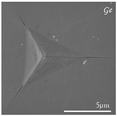


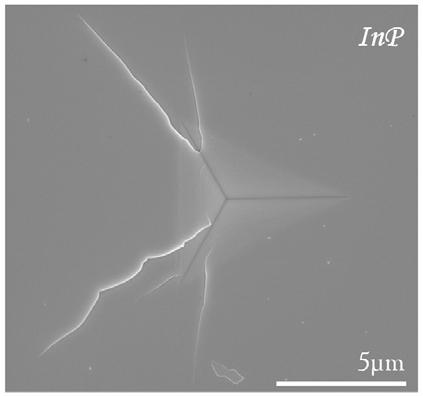
82 Figure SEM micrographs of indentations at an indentation load of 200mN. 142
83 Figure Schematic diagrams of a micro-raman spectrometer. The monochromatic incident beam is redirected through a set of optical components into the microscope objective. Objective is used for illuminating the sample and for collecting light scattered on the sample. Inelastically scattered light is then dispersed into a spectrum inside the Raman spectrometer unit. The computer collects Raman signal from the charged coupled device (CCD) detector attached to the spectrometer and optical images from the video camera attached to the microscope. 143
 produced with the load of 150mN (left) and 200mN (right) at the loading rate of 1mN/s and Raman spectra from the center of the")
84 Figure 3-18(a). Laser optical microscope images of Berkovich indentation on Si(100) produced with the load of 150mN (left) and 200mN (right) at the loading rate of 1mN/s and Raman spectra from the center of the indent. It shows that after nanoindentation, a single band of 520cm -1 of pristine Si surface (Si-I) has been replaced by multiple bands that belong to metasable phases, Si-III&Si-XII. 144
 produced with the load of 200mN at the loading rate of 1mN/s and")
85 Figure 3-18(b). Laser optical microscope images of Berkovich indentation on Ge(100) produced with the load of 200mN at the loading rate of 1mN/s and Raman spectra obtained from pristine Ge surface and presented the nanoindentation-induced crystalline metastable phase. 145
. 146")
86 Figure 3-18(c). Laser optical microscope images of Berkovich indentation on GaAs(100) produced with the load of 200mN at the loading rate of 1mN/s and Raman spectra from the center of the indent. There is a charge of the relative intensities and a shift of the Raman bands towards higher frequencies after nanoindentation (do not provide sufficient evidence of a phase transformation). 146

87 Figure 3-18(d). Laser optical microscope images of Berkovich indentation on GaN produced with the load of 200mN at the loading rate of 1mN/s and Raman spectra of the pristine surface and the residual impression of GaN. No manifestly phase transformation was occurred. 147
88 Figure 3-18(e). Berkovich indentation on GaSb produced with the load of 100mN at the loading rate of 1mN/s and Raman spectra of the pristine surface and the residual impression of GaSb. No manifestly phase transformation was occurred. 148
89 Figure 3-18(f). Berkovich indentation on InP produced with the load of 100mN at the loading rate of 1mN/s and Raman spectra of the pristine surface and the residual impression of InP. No manifestly phase transformation was occurred. 149

90 Figure Cross-sectional GaN preparation of nanoindentation by lift-out technique in FIB. 150
91 Figure 3-20(a). Schematic diagram of a Transmission Electron Microscopy. Figure 3-20(b). The scattering of an incident electron beam (I) by a crystal lattice. In the other side of sample, two kinds of intense beam can be found: the direct beam (T) and the diffracted beam (D). In N-direction, no intense electron beam will be detected. 151
92 Figure 3-20(c). Schematic diagram of electron diffraction in TEM. Figure 3-20(d). Diffraction contrast at an edge dislocation. The entire sample is set at an orientation close to Bragg condition; then the lattice on one side of the dislocation will be bent locally to the Bragg condition. The dislocation core will therefore diffract the beam strongly and appear dark on the bright field image. 152


93 (a) (b) (Continue) 153
 TEM plan view image of Si indented under 10mN; (b) BF and DF XTEM images of")
 and Diffraction pattern of crystalline Si-I taken from")
94 (c) (d) Figure (a) TEM plan view image of Si indented under 10mN; (b) BF and DF XTEM images of Si at an indentation load of 200mN; (c) Diffraction pattern of region I (directly under the indentation) and Diffraction pattern of crystalline Si-I taken from region II and (d) HRTEM image inside the transformation zone. 154


95 Figure BF XTEM image of indent in Ge at maximum indentation load of 150mN. Figure BF XTEM image of indent in GaAs at maximum indentation load of 150mN. 155


96 (a) (b) Figure BF XTEM images of indent in GaN at maximum indentation load of 200mN. 156


97 Figure BF XTEM images of indent in InP at maximum indentation load of 100mN. Figure BF XTEM images of indent in GaSb at maximum indentation load of 100mN. 157

98 Figure MD simulation model for GaAs nanoindentation. Red, green and blue represent the C, Ga and As atoms, respectively. 158

99 Figure Load-displacement data for GaAs obtained at 300K during nanoindentation with a Berkovich indenter showing pop-in behavior during loading and, the cross-sectional view of the (010) plane corresponds to II-V steps. Figure The load vs. displacement curve of GaAs nanoindentation at a temperature of 700K. 159


100 (Continue) 160

101 (Continue) 161
 3D MD simulation views of the dissociated dislocation loops at 300K and, the cross-sectional view of dislocation loops surrounded the indenter tip and rotating 30 along the [111] plane")
102 Figure (a) 3D MD simulation views of the dissociated dislocation loops at 300K and, the cross-sectional view of dislocation loops surrounded the indenter tip and rotating 30 along the [111] plane (corresponding to the IV step) at a penetration depth of 1.5nm and of 2nm in (b); (c) the top-view of contact surface; (d) schematic representation of the plastic zone structure and (e) 3D MD simulation views and the cross-sectional view of the dislocation structures/loops surrounded the indenter tip and rotating 30 along the [111] plane at 700K. 162