Investigation of thin-film CdTe/Ge tandem solar cells
|
|
|
- Poppy Tyler
- 5 years ago
- Views:
Transcription

1 Investigation of thin-film CdTe/Ge tandem solar cells Won-Jae Lee B.Eng, M.Eng. This thesis is presented for the degree of Doctor of Philosophy of The University of Western Australia School of Electrical, Electronic and Computer Engineering The University of Western Australia 2017
2
3
4
5 Abstract The rapid growth of the world s economy and population needs a tremendous amount of energy. Moreover, global warming, fossil fuel depletion and international conflict related with territories involving natural resources are a great concern all over the world. To solve these energy problems that the world is facing, the development of alternative energy sources is required. A thin-film based solar cell is one of the leading contenders for providing costeffective and pollution-free energy. Furthermore, the efficiency of thin-film solar cells can be improved with a tandem structure. This thesis describes the development of solar cells employing a tandem structure with CdTe and Ge thin films, from crystallization of thin film materials to simulation of tandem solar cell performance. The cost-effective use of materials is essential if the solar cell industry is to provide energy cheaper than fossil fuel sources. In order to render the fabrication process low-cost and simple, poly-ge thin films have been investigated using electron beam (E-beam) evaporation and solid phase crystallization (SPC). For all crystallized Ge thin films as a photovoltaic material, the electrical properties were found to improve with increasing SPC temperature. After crystallization of the Ge layer through annealing at 600 C, p-ge/n-si heterojunction devices obtained an on/off current ratio of 10 6, an ideality factor of 1.25, and a built-in potential of 0.58eV. The improvement in device performance is correlated with the degree of crystallization of the Ge thin film, which indicated that it can be considered as a suitable candidate for optoelectronic applications. For CdS/CdTe solar cells, n-type CdS thin films for use as a window layer were prepared and investigated using thermal evaporation and various characterization techniques. It is found that post-deposition annealing temperature is more effective than deposition substrate temperature in improving the electrical and optical properties of the CdS thin films. For the case of increasing substrate temperature during deposition, the formation of defects is determined by the effective Cd/S ratio, whereas the post-deposition annealing temperature determines defect migration and annihilation, which have a strong influence on the electrical
6 vi and optical properties of CdS thin films. The electrical and optical properties of CdS thin films obtained herein are shown to be suitable for thin-film solar cell applications, which is demonstrated by fabricating n-cds/p-si and CdS/CdTe heterojunction devices. To form the absorber in CdS/CdTe solar cells, CdTe films were deposited by thermal evaporation in a high vacuum onto CdS/ITO/glass substrates in superstrate configuration. The CdTe layers were then recrystallized with CdCl 2 and annealed in air. The properties of CdTe films were found to improve at higher deposition substrate temperature and with CdCl 2 treatment. In the n-cds/p-cdte heterojunction solar cells, the photovoltaic cell parameters indicated that deposition of CdS films at room temperature resulted in higher performing cells; with the substrate temperature required during thermal deposition of CdTe acting to effectively anneal the underlying CdS thin film. Under 1 sun illumination (AM 1.5G), the fabricated solar cells achieved a highest efficiency of > 11% with MgF 2 anti-reflection coating, a short-circuit current of 24.16mA/cm 2, and an open-circuit voltage of 0.765V. Since the experimental effort required to optimize the overall fabrication process and tunnel junctions are beyond the scope of this project, the CdTe/Ge tandem solar cells were modeled by incorporating possible improvements as well as experimental data to improve the modeling conditions and achieve realistic outcomes. One approach applied to model the tunnel junction is the use of a-si:h as the p+ recombination layer and a Ge n+ layer. The calculated highest performance of the tandem cells was around 25.3% in efficiency with V oc = 1.2V, J sc = 26.3mA/cm 2, and FF = 81.9%. For stand-alone cells, the efficiency of the CdTe top cell is 21.12% (V oc = 0.98V, J sc = 26.3mA/cm 2, and FF of 81.9%), and the efficiency of the Ge bottom cell is 4.58% (V oc = 0.25V, J sc = 27.7mA/cm 2, and FF of 66.13%). This thesis has proposed and laid the groundwork for further development of a novel thin-film tandem solar cell structure, consisting of the combination of a thin-film CdTe solar cell, a tunnel junction and a crystallized thin-film Ge solar cell. Via experimental results and comprehensive device modeling, it has been shown that tandem cell device efficiencies approaching or exceeding 25% are achievable.
7 Acknowledgements First of all, I would like to thank Prof. Lorenzo Faraone, Prof. John Dell and Prof. Gilberto Umana-Membreno for their support, advice and supervision of my doctoral thesis, and with allowing me to study with excellent facilities on the beautiful campus at the University of Western Australia. I would like to thank all current and former MRG members listed in random order below for support and fruitful discussions (Ms. Sabina Betts, Dr. Dilusha Silva, Dr. Jarek Antoszewski, Dr, Mariusz Martyniuk, Dr. Fei Jiang, Dr. Gino Putrino, Dr. Wen Lei, Dr. Yongling Ren, Dr. Adrian Keating, Dr. Renjie Gu, Dr. Nima Dehdashti, Ms. Karen Kader, Jing Zhang, Nir Zvison, Hemendra Kala, Haifeng Mao, Farah Muhammad Khir, James Sharp, Dhirendra Tripathi, Radha Krishnan Nachimuthu, Rohit Sharda, Anna Podolska, Amit Choudhary, Balaji Sankarshanan, Ben Cheah, Imtiaz Madni, Michal Zawierta, Xiao Sun). I would like to thank many people who I met and had a good time with in Perth listed in random order (Dr. Kim Young-ho, Lee Joonmo, Kanchan Chaudhury, Patrick Ho, Dr. Jang Ugeun, Dr. Oh Se-Heon, Dr. Rhee Jonghwan, Prof. Eun-Jung Holden, Prof. Lee Mi-kyung, Dr. Lee Jong-Ku, Dr. Moon Seongkon, Dr. Choi Yusuk, Dr. Kim Duyong, Jeon Minjung, and their families). I would also like to thank my wife s previous bosses and friends (Chloe Lee, Hally Kim and their families). I am sorry if I did not mention all of you, but I really appreciate all of you. Last but not least I would like to thank my wife, Mijin Kwon, for her support during my PhD years, and my beloved family including my little son, parents and brother.
8
9
10
11 Table of contents Table of contents xi List of figures xv List of tables xxi 1 Introduction Motivation World energy demand Solar energy Background Solar cell physics and operation Thin-film solar cells (TFSCs) Tandem (multi-junction) solar cells Toward CdTe/Ge tandem solar cells Required specifications (see Fig. 1.19) Thesis outline and scope Review of CdTe and Ge single and tandem solar cells CdTe solar cells Highest efficiency CdTe solar cells on flexible substrates Ge solar cells Highest efficiency Ge-on-glass solar cells CdTe/Ge tandem solar cells... 31
12 xii Table of contents 2.4 Summary and discussion Experimental and characterization techniques Review of deposition methods Ge deposition techniques CdS deposition techniques CdTe deposition techniques Substrate preparation Structural characterization X-Ray Diffraction (XRD) Scanning Electron Microscopy (SEM) Electrical characterization Hall effect Current-voltage (I-V) Capacitance-voltage (C-V) Optical characterization Spectroscopy for optical properties Spatial photocurrent mapping Summary Thin film Ge and devices Introduction Ge thin film deposition and device preparation Characterization of crystallized Ge thin films Hall effect measurement SEM analysis XRD analysis Optical transmission Characterization of crystallized Ge/Si hetero-junction diodes I-V measurements C-V measurements Spatial photocurrent map Summary and discussion... 78
13 Table of contents xiii 5 Thin film CdS and devices Introduction CdS thin film deposition and device preparation Characterization of evaporated CdS Hall effect measurement SEM analysis X-Ray Diffraction Optical characterization Characteristics of CdS/Si hetero-junction devices Summary and discussion Thin film CdTe and devices Introduction Technological challenges CdTe thin film deposition and device preparation Characterization of evaporated CdTe X-Ray Diffraction Optical transmittance SEM image analysis The role of CdCl 2 treatment Effect of CdCl 2 treatment on device properties Summary and discussion Performance of CdS/CdTe solar cells Back contact Back contact on CdTe films Contact improvement with Cu Spice modeling of back-contact effect in solar cells Effect of CdS window layer Role of CdS film as a window layer Effect of CdS film preparation on photovoltaic properties Optical losses Reflection losses
14 xiv Table of contents Anti-reflection coating using MgF Summary Potential and limitations of CdTe/Ge tandem solar cells Obstacles limiting high-efficiency CdTe/Ge tandem solar cell technologies Requirements for the CdTe top cell Tunnel junction or recombination layer Ge bottom cell Simulation of CdTe/Ge tandem cells Summary and discussion Summary, conclusions and future work Summary and conclusions Future work Appendix A Updating scanning laser microscopy (SLM) system 149 A.1 Updating SLM machine A.2 Measurements A.2.1 Laser beam induced current (LBIC) A.2.2 Spatial photocurrent mapping A.2.3 Carrier lifetime Appendix B Publications arising from this thesis 155 References 157
15 List of figures 1.1 World population growth Global GDP growth estimated by Oxford Economics, IMF World Economic Outlook Comparison of various energy sources Global (AM0 and AM1.5G) standard spectrum Spectrum of the radiation interrupted by the earth s atmosphere The path length in units of Air Mass, changes with the zenith angle Bandgap structure and a solar cell with a resistive load Solar cell voltage-current characteristic under illumination Equivalent circuit of a solar cell Best efficiency research solar cells Flexible thin film solar cell Solar PV crystalline silicon and thin-film module cost learning curve Absorption coefficient of various materials Maximum theoretical efficiency (Shockley Queisser limit) for thin film solar cells Losses by thermalization and non-absorption of low-energy-photons Absorption of solar spectrum by different energy bandgap materials in a tandem solar cell Tandem solar cell operation with different connection (parallel and serial connection) The maximum efficiency for a double-junction tandem cell under the AM1.5G spectrum Band diagram for a tunnel junction and details of a tandem structure Chapter description illustrated through a CdTe/Ge tandem cell structure.. 19
16 xvi List of figures 2.1 The best efficiency of CdTe solar cells and modules Fabrication methods for thin film solar cells J-V comparison between the best efficiency record and SQ limits Quantum efficiencies of record cells Quantum efficiencies of milestone cells on flexible substrates I-V measurement of the highest efficiency Ge solar cell Phosphorous diffusion into Ge at different temperature and time Fabrication and characteristics of Ge-on-glass solar cells A suggested structure of CdTe/Ge tandem solar cells Schematic illustration of solid phase crystallization processes in a-si Phase diagram describing crystal status of 200 nm thick undoped Ge films processed by MIC technique Operation of electron beam evaporation Operation of thermal evaporation Schematic diagram of various techniques for CdTe thin film deposition Measured optical properties of various substrates X-ray diffraction Ge surface image by SEM with short working distance and low acceleration voltage Geometry for measuring the Hall effect Schematic diagrams of resistivity and Hall effect measurements by the van der Pauw method The 2T Hall effect measurement setup Extraction of ideality factor with modeling Extraction of parasitic resistances (R s and R sh ) under illumination) Photovoltaic I-V curve under illumination A typical graph of 1/C 2 versus voltage Schematic diagram of SLM system for 2D current mapping Pinholes on Ge thin films prepared at high deposition rate Schematics of a poly-ge heterojunction device on silicon substrate Mask design for fabrication of p-ge/n-si devices... 66
17 List of figures xvii 4.4 Results of Hall-effect and resistivity measurements on Ge thin films deposited on glass substrates SEM images of 600 nm thick Ge films deposited and annealed on silicon SEM images of 1 μm and 200 nm thick Ge films deposited and annealed on glass Cross-sectional SEM images of 1 μm thick Ge films deposited on glass slides XRD spectra of crystallized Ge thin films Optical transmittance spectra of crystallized Ge annealed for 30min Bandgap structure of a single crystalline Ge/Si junction Current-voltage characteristics of p-ge/n-si heterojunction diodes as a function of annealing temperature Experimental 1/C 2 versus reverse bias characteristics for the p-ge/n-si diodes D spatial photocurrent maps of p-ge/n-si heterojunction devices Measured photocurrent for 100 nm p-ge/n-si devices with transmission of 100 nm thick crystallized Ge thin film and absorption of 100 nm p-ge/n-si modeled using optical properties of single crystal materials The mask design and schematic diagram for fabrication of n-cds/p-si heterojunction device Hall effect measurements on evaporated CdS films SEM surface images of CdS thin films Cross-sectional SEM images of CdS thin films SEM images of CdS thin films deposited and annealed on silicon substrates XRD spectra of CdS thin films Transmission spectra of 1μm thick CdS thin films on glass slides Extraction of optical bandgap for CdS films Refractive index as a function of temperature I-V curves of Ohmic contacts formed using aluminum on both n-cds films and p-si substrates I-V characteristics of CdS/Si heterojunction devices A 3.5μm thick CdTe film with absorption coefficient... 98
18 xviii List of figures 6.2 Mask design and schematic diagram for fabrication of CdS/CdTe heterojunction devices SEM images for n-cds/p-cdte heterojunction solar cell on ITO-coated glass XRD spectra of CdTe thin films Optical transmission of 1 μm thick CdTe thin films on glass slides SEM images of CdTe thin films on glass slides XRD spectra of CdTe films with and without CdCl 2 treatment SEM surface images of CdTe thin films on glass slides I-V characteristics of CdS/CdTe devices with and without CdCl 2 treatment Energy band diagram of semiconductor-metal junction Experimental back-contact barrier effects on solar cell parameters A two-diode equivalent circuit model for the CdS/CdTe solar cell Spice modeling to extract back-contact barrier of two different solar cells with different back contacts Calculated barrier height extracted from the contact saturation current Role of CdS thin films Representative photovoltaic I-V curves under 1 sun illumination Experimental photovoltaic properties (V oc,j sc, FF and efficiency) of solar cells Structure with multiple thin film layers Optical properties of a fabricated CdS/CdTe solar cell with modeling data Experimental optical transmission and absorption of CdTe solar cells as a function of thickness of MgF 2 AR coating Observed improvement in CdTe solar cell performance with an optimized thickness (70nm) of MgF 2 AR coating Observed improvement in solar cell parameters due to the application of an anti-reflection coating Typical I-V characteristics of fabricated solar cells Optical constants for modeling, and comparison of modeled optical properties with experimental data Modeled absorption in CdS and CdTe layers as a function of CdS film thickness
19 List of figures xix 8.3 Modeled solar spectra absorbed in CdTe layer and generated photocurrent as a function of thickness of CdS thin films Calculated open-circuit voltage as a function of carrier concentration of CdTe film Simulation of solar cell performance using the high J sc and high V oc Measured optical properties of CdTe solar cells Modeled optical properties of CdTe solar cells with ITO/TiO 2 double TCO layer Tandem cell structure and energy band diagram for CdTe/Ge solar cell Modeled photocurrent and absorption of the solar spectrum as a function of Ge thickness Modeled quantum efficiency of CdTe top cell and Ge bottom cell Modeled photovoltaic properties of CdTe/Ge tandem solar cells and individual top and bottom cells A.1 Schematic diagram of SLM system A.2 Noise improvement after replacement of old parts A.3 Temperature calibration for precise measurement A.4 Specific device geometry to measure LBIC A.5 Specific device geometry to measure spatial photocurrent A.6 Specific device geometry to measure transient carrier lifetime
20
21 List of tables 1.1 Confirmed terrestrial solar module efficiencies measured under the AM1.5G spectrum Required specifications for a CdTe/Ge tandem cell Photovoltaic properties of the best cell and module A comparison of flexible cells with record device parameters Predicted photovoltaic performance of the CdTe/Ge tandem cell in the previous work Summary of Ge crystallization using a variety of techniques Optical bandgap of sputtered CdS films Specifics of various substrates Summary of properties of Ge thin films crystallized using various techniques Extracted diode ideality factor, built-in potential and n-si doping concentration of p-ge/n-si devices Extracted energy bandgap of CdS thin films at different deposition and annealing temperatures Extracted solar cell parameters dependent on CdCl 2 treatment Layer properties for simulation Ge properties for simulation Modeled results of tandem solar cell and individual top and bottom cells.. 143
22
23 Chapter 1 Introduction 1.1 Motivation World energy demand If the 20 th century was the era of the Cold War, energy has become the next battlefield since the late 20 th century as countries seek to protect their natural resources [1]. Use of energy is necessary to sustain human life and economic development. However, global warming, fossil fuel depletion, and international conflict are associated with this energy use [1, 2]. Worldwide energy consumption was around 12,730.4 Mtoe (toe : Tonnage of Oil Equivalent) in 2013, with approximately 87% of this sourced from the combustion of fossil fuels [3]. The world s growing population, as well as an increase in the average gross domestic product (GDP), will lead to an ongoing increase in energy consumption [4]. Moreover, the world s population (see Fig. 1.1) is expected to reach 9 billion between 2040 and 2050 [5], and the average world GDP (see Fig. 1.2) is increasing at 3-4% annually, as predicted by the International Monetary Fund (IMF) [6]. Thus, world energy demand is increasing, driven by population and world GDP growth, and is estimated that it will reach 18,000 Mtoe by 2035 [3, 7]. This continuous increase in the world s energy demand and consumption seems unavoidable in the near future. Similarly, global warming will eventually lead to substantial changes in the world s climate, if most of the energy is generated by the combustion of fossil fu-
![2 Introduction Fig. 1.1 World population growth [8]. Fig. 1.2 Global GDP growth estimated by Oxford Economics, IMF World Economic Outlook, EIU [9]. els [10].](/docs-images/89/99019561/images/24-0.jpg "In spite of this, the current world s use of renewable energy sources, such as wind, solar, biofuels, wave, tidal and geothermal power, account for just 2.")
![4% of total energy generation capacity, excluding hydro [3].](/docs-images/89/99019561/images/24-1.jpg "Therefore, renewable energies such as solar and wind need to be advanced if we are to reduce the use of fossil fuels, and save our environment. 1.")
24 2 Introduction Fig. 1.1 World population growth [8]. Fig. 1.2 Global GDP growth estimated by Oxford Economics, IMF World Economic Outlook, EIU [9]. els [10]. In spite of this, the current world s use of renewable energy sources, such as wind, solar, biofuels, wave, tidal and geothermal power, account for just 2.4% of total energy generation capacity, excluding hydro [3]. Therefore, renewable energies such as solar and wind need to be advanced if we are to reduce the use of fossil fuels, and save our environment Solar energy In 14 and a half seconds, the sun provides as much energy to Earth as Humanity uses in a day. Ramez Naam Scientific American The available energy from the sun is orders of magnitude larger than all other energy
![1.1 Motivation 3 Fig. 1.3 Comparison of various energy sources [2]. sources, as evident from Fig. 1.3. Even a small fraction of the available solar energy reaching the earth s surface would be enough to satisfy the expected global energy demand.](/docs-images/89/99019561/images/25-0.jpg "Solar energy is the only renewable source that can meet world energy consumption with a small fraction of the available total [2].")
25 1.1 Motivation 3 Fig. 1.3 Comparison of various energy sources [2]. sources, as evident from Fig Even a small fraction of the available solar energy reaching the earth s surface would be enough to satisfy the expected global energy demand. Solar energy is the only renewable source that can meet world energy consumption with a small fraction of the available total [2]. Furthermore, solar energy is virtually infinite and clean, which can solve our environmental problems as well. Radiation from the sun sustains life on earth and controls climate. The sun has a surface temperature of around 5800K, so the spectrum of the radiation from the sun is similar to that of a 5800K blackbody [11]. The values of irradiance from the sun on the outer atmosphere are about 1360 W/m 2 [12]. Most of the energy from the sun is concentrated in the visible and near-visible range of the spectrum, as shown in Fig The visible light, between 380 and 780 nm, represents 48% of the total energy from the sun. Shorter wavelength ultraviolet (UV) accounts for 6.4% of the total. The remaining 45.6% of the radiant energy is spread over the infrared region [13]. Various components of the earth s atmosphere prevent solar radiation from penetrating it and reaching the earth s surface, since some of the radiation is absorbed and scattered by the atmosphere. Oxygen and nitrogen absorb very short wave radiation. Ultraviolet (UV) radiation is blocked by ozone in the atmosphere and some of it reaches the earth s surface.
26 4 Introduction Fig. 1.4 Global (AM0 and AM1.5G) standard spectrum [14]. Fig. 1.5 Spectrum of the radiation interrupted by the earth s atmosphere [18]. Water vapor, carbon dioxide and, to a lesser extent, oxygen, selectively absorb in the near infrared [15] as shown in Fig As a result of reflection, scattering, and absorption of radiation, the solar energy that reaches the earth s surface is much reduced in intensity. The energy associated with direct sunlight thus depends on the altitude of the sun, and also varies with such factors as latitude, season, and cloudiness [15 17]. Particularly these seasonal- and daytime-dependent variations of the sun spectrum will affect current matching in a tandem structure, thus reducing efficiency more than single cells.

27 1.1 Motivation 5 Fig. 1.6 The path length in units of Air Mass, changes with the zenith angle. The atmospheric path for any zenith angle is simply described relative to the overhead air mass as shown in Fig This pathlength can be approximated by 1/cosθ z, where θ z is the angle between the sun and the point directly overhead [16, 19]. Therefore: AM = 1/cosθ z (1.1) The spectrum outside the atmosphere is designated by Air Mass zero (AM0) because it passes through no air mass. Air Mass 1 Direct (AM1D, θ z = 0) is direct radiation that reaches the ground after passing through the entire atmosphere overhead. The direct portion of the solar radiation is collimated with an angle of approximately 0.53 (full angle), while the "diffuse" portion is incident from the hemispheric sky and from ground reflections and scatter [20]. The standard spectrum at the Earth s surface is called AM1.5G ("Global" which includes both direct and diffuse radiation, θ z = 48.19) or AM1.5D (direct radiation only). AM1.5G has been calculated to be approximately 970 W/m 2, which has been standardized as 1 kw/m 2 (equal to 100 mw/cm 2 ) when used for rating photovoltaic products. Therefore, the sun provides 1 kw/m 2 of free, non-polluting power for several hours every day [16, 17, 19]. However, as shown in Table 1.1, the highest efficiency of commercial solar modules produced in industry is still less than 20% especially for multi-crystalline materials, and there is much scope for converting more solar energy into electricity [21, 22]. Therefore, technologies for converting solar energy into electricity need to be improved. Some new and
28 6 Introduction Table 1.1 Confirmed terrestrial solar module efficiencies measured under the global AM1.5 spectrum (1000 W/m 2 ) [21]. Material Eff.[%] Area(cm 2 ) V oc [V] I sc [A] FF Si (crystalline) Si (large crystalline) , Si (multi-crystalline) , GaAs (thin film) CdTe (thin film) CIGS (Cd free) CIGS (thin film) , a-si/nc-si (tandem) , Organic emerging developments, such as organic and multi-junction solar cells, have the potential to change the situation [21 25]. 1.2 Background Solar cell physics and operation An inorganic photovoltaic cell is basically a semiconductor diode that converts sunlight directly into electricity [17, 26 28]. When a photon with energy greater than the bandgap is absorbed, it can induce electron-hole pairs by excitation of electrons out of the valence band into the conduction band as depicted in Fig. 1.7a. In the second step of the energy conversion process, the photogenerated electron-hole pairs are separated by the internal electric field in the space-charge layer of the diode structure of the solar cell with electrons drifting to one of the electrodes and holes drifting to the other electrode with diffusion becoming crucial in carrier transport at the neutral region. Fig. 1.7b shows a solar cell with a resistive load. When light is incident through the window layer, the electron-hole pairs generated in the absorber layer will be swept out of the layer to produce the photocurrent J ph due to the electric field. As a consequence, J ph produces a voltage drop across the resistive load. The net current of this pn-junction solar cell, is ( ) ] ev J = J F J ph = J 0 [exp 1 J ph (1.2) nkt when the ideal-diode equation is used. The forward-bias voltage produces a forward-bias current J F with a direction opposite to J ph.
, open-circuit voltage (V oc ), fill factor (FF) and conversion")
29 1.2 Background 7 (a) (b) Fig. 1.7 (a) Bandgap structure, (b) A solar cell with a resistive load. The primary parameters employed to describe the performance of a photovoltaic device are the short-circuit current density (J sc ), open-circuit voltage (V oc ), fill factor (FF) and conversion efficiency (η). J sc is the current density that flows through the junction under illumination under short circuit condition (bias is never applied to a solar cell). In the ideal case it equals the photogenerated current density (J ph ) and is proportional to the incident number of photons or, alternatively, the intensity of illumination. V oc is the voltage across the junction when the current through the junction is zero (i.e. open, no circuit load), and can be expressed as V oc = nkt ( ) e ln Jph + 1 J 0 (1.3) by rearranging equation 1.2 with J = 0. The point on the J V curve that yields the maximum power is referred to as the maximum power point (mp), the corresponding current density and voltage are J mp and V mp as shown in Fig The fill factor (FF) is a measure of the
 The standard test conditions are when P sun is 100 mw/cm 2 of a normally incident air-mass (AM) 1.5 spectrum at 25 C.")
30 8 Introduction Fig. 1.8 Solar cell voltage-current characteristic under illumination. "squareness" of the J V curve, and is given by FF = V mpj mp V oc J sc (1.4) The standard test conditions are when P sun is 100 mw/cm 2 of a normally incident air-mass (AM) 1.5 spectrum at 25 C. The efficiency of a solar cell is defined as the ratio of the maximum output power P max to the input power (incident power) P incident, and can be expressed as η = P max P incident = V ocj sc FF p incident (1.5) A real solar cell has a parasitic series resistance (R s ) and shunt resistance (R sh ). There are several physical mechanisms responsible for these resistances. Series resistance R s is composed of the bulk resistance of the semiconductor materials and the resistance of the front and back contacts. Shunt resistance R sh is caused by leakage across the p n junction and around the edge of the cell. An ideal cell will have infinite shunt resistance (R sh = ) and zero series resistance (R s = 0). A modest value of R s mostly affects the far forward voltage region above V mp, whereas the open circuit voltage is not affected by R s because no current flows at V oc. The influence of R sh is visible in the low voltage range (near zero and reverse voltage). Both, R s and R sh can reduce the FF by a predictable amount. High values of R s and low values of R sh can also reduce J sc and V oc, respectively. Under illumination, the J-V
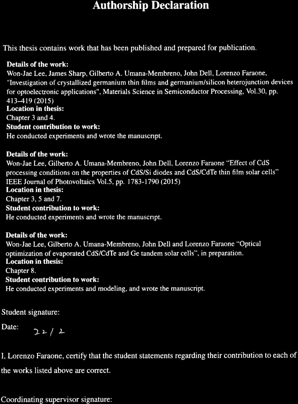
31 1.2 Background 9 characteristics of a solar cell with parasitic resistance can be described by ( ) ] e(v Rs J) J = J 0 [exp 1 J ph + (V R sj) (1.6) nkt R sh The electronic behavior of such a solar cell can be represented by an equivalent circuit model, shown in Fig. 1.9, based on discrete electrical components. The photo-generation mechanism is represented by the current generator, and the dark current is represented by the diode which is oriented opposite to the current generator. The resistor parallel to the diode represents the shunt resistance R sh and the resistor that is in series with the rest of the circuit represents the series resistance R s. Fig. 1.9 Equivalent circuit of a solar cell Thin-film solar cells (TFSCs) Thin-film solar cells (TFSCs) have improved significantly over the years, with efficiencies approaching 23% in 2017, including cadmium telluride (CdTe) : 22.1%, copper indium gallium diselenide (CIGS) : 22.6%, and amorphous thin-film silicon (a-si) : 14%, as shown in Fig The general advantages of thin-film technologies over crystalline silicon relate to the simple deposition processes on large area and cheap substrates such as glass, lower material consumption, and the possibility of using flexible substrates in roll-to-roll processes as shown in Fig [29]. Thin-films can be deposited by various techniques, both physically and chemically. Film thickness varies from a few nanometers (nm) to tens of micrometers (μm), much thinner than conventional poly-silicon solar cells which are hundreds of micrometers (μm) thick. Therefore, thin film technologies allow solar cells to be flexible, portable and stackable. All photovoltaic (PV) technologies are focused on low-cost and high-conversion efficiency. In this respect, thin film PV technology is the best candidate,


32 10 Introduction Fig Best efficiency research solar cells [30].
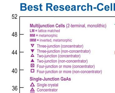
![1.2 Background 11 Fig. 1.11 Flexible thin film solar cell [31].](/docs-images/89/99019561/images/33-0.jpg "because thin-film solar cells can be produced using cheap large-area deposition techniques and low-cost substrates combined with schemes of monolithically interconnecting solar cells in series for")
33 1.2 Background 11 Fig Flexible thin film solar cell [31]. because thin-film solar cells can be produced using cheap large-area deposition techniques and low-cost substrates combined with schemes of monolithically interconnecting solar cells in series for high efficiency [32]. Fig shows exactly cost effectiveness of thin-film solar cells in module price compared to c-si solar cells. Conventional c-si PV modules are the most expensive PV technology, although they have the highest commercial efficiency. However, CIGS modules are approaching the efficiency levels of c-si modules [33]. Therefore, advantage of thin-film solar cells on manufacturing cost is unquestionable. In thin film solar cells, the absorber is the most important layer where the absorbed light generates pairs of free electrons and holes, which can then be extracted to the contacts and Fig Solar PV crystalline silicon and thin-film module cost learning curve [33].
![12 Introduction Fig. 1.13 Absorption coefficient of various materials [34]. can contribute to the electrical current (photocurrent of the device).](/docs-images/89/99019561/images/34-0.jpg "Thus, the layers must absorb as much light as possible and be fabricated as thin as possible. The absorber layer thickness is dependent on the absorption coefficient of the materials, as shown in Fig.")
34 12 Introduction Fig Absorption coefficient of various materials [34]. can contribute to the electrical current (photocurrent of the device). Thus, the layers must absorb as much light as possible and be fabricated as thin as possible. The absorber layer thickness is dependent on the absorption coefficient of the materials, as shown in Fig The absorption coefficient in the semiconductor is a very strong function of photon energy and bandgap energy. The intensity of the photon flux decreases exponentially with distance through the semiconductor material. The relation between an incident photon intensity, I 0, and the photon flux at a position x, I(x), can be given by I(x)=I 0 exp αx (1.7) where α is the absorption coefficient and x is the material thickness. Thus, for an absorption coefficient of cm 1, a film 2.3 μm thick absorbs about 90% of incident light. In order to achieve the high absorption of light and reduction of layer thickness at the same time, the materials must have a high absorption coefficient. Since thin film solar cells consist of more than two thin layers, optical losses such as a reflection loss in devices and optical absorption loss in window layers need to be reduced. Commonly, an anti-reflection coating is deposited on thin-film solar cells using low refractive index materials such as MgF 2 to reduce the reflectance loss. TCO (transparent conductive oxide) is generally used as a front contact in thin film solar cells, which need to have high conductivity and transparency to improve efficiency of thin film solar cells by preventing any
![1.2 Background 13 optical losses [35]. 1.2.3 Tandem (multi-junction) solar cells The theoretical maximum efficiency of single-junction cells has been calculated as a function of bandgap energy, as depicted in Fig.](/docs-images/89/99019561/images/35-1.jpg "1.14 [36, 37]. The two main mechanisms limiting solar cell efficiency are; losses by thermalization, and non-absorption of low-energyphotons.")
35 1.2 Background 13 optical losses [35] Tandem (multi-junction) solar cells The theoretical maximum efficiency of single-junction cells has been calculated as a function of bandgap energy, as depicted in Fig [36, 37]. The two main mechanisms limiting solar cell efficiency are; losses by thermalization, and non-absorption of low-energyphotons. In the case of thermalization, the excess energy of absorbed photons is transferred to the active material via phonons. This energy is effectively lost to the photovoltaic conversion process. In contrast, photons with energy lower than the bandgap cannot be absorbed (see Fig. 1.15) [38]. Therefore, in single cell devices, a trade-off has to be found between Fig Maximum theoretical efficiency (Shockley Queisser limit) for thin film solar cells under AM1.5 illumination. Note that the bandgap of the CIGS system can be tuned by controlling the In/Ga ratio [37]. Fig Losses by thermalization and non-absorption of low-energyphotons.


36 14 Introduction thermalization loss and non-absorption loss minimized by using wide and narrow bandgap materials, respectively. One promising approach to improve the efficiency of thin film photovoltaic devices is multi-junction solar cells, which are comprised of a stack of devices made of different materials. The idea of a tandem cell is to achieve higher absorption efficiency using materials with different bandgaps. One material is optimized to collect the higher energetic photons and the other, with a narrower bandgap than the first one, is optimized to absorb photons with lower energy [39]. Fig shows the ideal picture of the relation between the absorption spectra of the three solar cells used in a triple-junction tandem cell. As shown in Fig. 1.16b, each solar cell with different bandgap material in a tandem solar cell absorbs and produces electrical current in response to different wavelength of light. The efficiency of this triple-junction tandem solar cell shows higher efficiency via absorption of wide range of solar spectrum. Therefore, it is possible to enhance the efficiency by balancing the optical (a) (b) Fig (a) Absorption of solar spectrum by different energy bandgap materials in a tandem solar cell, (b) Spectra absorption on each component cell in a tandem solar cell.

37 1.2 Background 15 and electrical properties of each cell in a tandem cell. There are two different methods to connect component cells: parallel or serial connections. For parallel connections [see Fig. 1.17, left-hand side], intermediate electrodes ensure charge collection for each individual cell. These back and front electrodes have to be transparent to minimize photon losses and highly conducting to maximize charge carrier collection. An obvious material for such electrodes would be a transparent conductive oxide (TCO). Serial connection is more realizable (see Fig. 1.17, right-hand side), since it only requires thin, non-continuous, non-absorbing metallic layers (tunnel or recombination layers) to match currents of the different cells and collect the carriers at two electrodes. Tandem cells in this thesis represent series connection only (monolithic tandem cell) fabricated by stacking one solar cell on top of the other. Although power conversion efficiency of solar cells has been increasing steadily (as shown in Fig. 1.10) and their production costs have been decreasing, there is still further room for improvement (for example, there is 10% absolute efficiency gap in CdTe solar cells between practical and theoretical efficiency as shown in Fig and Fig respectively). With increasing efficiency of individual solar cells, tandem solar cells will provide more opportunities to improve the overall efficiency by combining these cells. Fig Tandem solar cell operation with different connection (parallel and serial connection).

38 16 Introduction 1.3 Toward CdTe/Ge tandem solar cells The efficiency of CdTe solar cells has reached beyond 20% in 2014 through over 40 years research, as shown in Fig Since it is difficult to improve solar cell efficiency within a short time period, attempts to achieve higher efficiency solar cells have generally taken the paths of: using novel materials (such as : Perovskites) and development of tandem cells combining semiconductor materials with different energy bandgaps. In this work, a tandem cell structure that utilizes Ge as a bottom cell and CdTe as a top cell is proposed. All materials (CdS, CdTe and Ge) can be deposited by simple thermal evaporation and recrystallized by thermal annealing to make the thin films required by solar cells. This process has been demonstrated in previous work over a wide range of temperatures, lending credence to the viability of a CdTe/Ge/low-cost-substrate structure. Although the bandgap of CdTe ( 1.45 ev) and Ge ( 0.67 ev) are not optimal for a double-junction tandem cell due to photocurrent mismatching, as shown in Fig. 1.18, more than 30% can be achieved theoretically, and they can serve as the basis for the development of triple-junction solar cells. Since the data in Fig were calculated using bandgaps of materials without any optical and electrical losses [41], optical and electrical properties should be considered together in practice and modeling. In the modeling results, which will be presented in Chapter 8, it will be shown that current matching between a CdTe top cell and a Ge bottom cell can be optimized by controlling the thickness of the individual absorbers. It should be noted that the tandem-cell structure proposed in this thesis is formed employing thin-film technologies, Fig The maximum efficiency for a double-junction tandem cell under AM1.5G spectrum [40]
39 1.4 Required specifications (see Fig. 1.19) 17 and should be realizable using deposition techniques that are, in principle, much simpler and lower cost than those used for the fabrication of tandem cells based on ternary and quaternary single-crystal semiconductors. The success of a tandem cell depends not only on photocurrent matching, but also on ensuring that the interface between the two cells allows continuity of the photocurrent. This is usually achieved by creating a tunnel junction at the interface. In such a junction, the holes constituting the photogenerated current in the top cell recombine, via band-to-band tunneling, with photogenerated electrons from the bottom cell. Such a tunnel junction can often be formed using degenerately doped regions. 1.4 Required specifications (see Fig. 1.19) In order to optimize the tandem cell, the basic parameters (thickness and doping concentration) listed in Table 1.2 and Fig. 1.19b need to be realized. The equilibrium band-diagram for the tunnel junction is shown in Fig. 1.19a. The n+ emitter of the Ge cell forms one side of the tunnel junction, and a p+ CdTe region was introduced to form the other side. These parameters are for the basic tandem structure to be fabricated with an expected improvement in photovoltaic conversion efficiency up to a value in excess of 20% modeled in previous work [42]. However, as the record efficiency of solar cells continues to be improved and several requirements are not practical, such as p+ CdTe layers, the expected efficiency needs to be confirmed through experimental data. The achievable properties of thin films for tandem cells will be demonstrated and modeled more thoroughly throughout this thesis. Table 1.2 Required conditions for a CdTe/Ge tandem cell. Individual cell Layers Doping Thickness Top cell n-cds cm nm p-cdte cm μm Tunnel junction p+ CdTe > cm 3 50nm n+ Ge > cm 3 50nm Bottom cell n-ge cm 3 100nm p-ge cm μm
40 18 Introduction (a) (b) Fig (a) Band diagram for the tunnel junction and (b) details of a proposed tandem structure [42]. 1.5 Thesis outline and scope This thesis was part of a larger project that aims to determine the viability of practical CdTe/Ge thin film tandem solar cells. While the thin film solar cells should be comprised of either single-crystalline or poly-crystalline thin films, work presented in this thesis is restricted to poly-crystalline to demonstrate cost-effective techniques using a simple evaporation system. The objective of the present work was to overcome the limitations of solar cell efficiency through a tandem structure. Device structures and processing methods were developed to reduce the optical and electrical losses and enable the production of low-cost photovoltaics with high conversion efficiency. This thesis consists of 9 chapters addressing different aspects of the CdTe/Ge thin film tandem solar cell as shown in Fig

, and to characterize their properties for fabrication of tandem solar")
41 1.5 Thesis outline and scope 19 Chapter 2 : A literature review is presented in this chapter to understand previous process development of CdTe and Ge stand-alone solar cells, and CdTe/Ge tandem solar cells. For CdTe solar cells, the process development from the early stage of devices through to the present technology is reviewed. Since there is only one paper regarding CdTe/Ge tandem solar cells and few papers on Ge solar cells, the proposed design of tandem cells and process methods of Ge cells in the papers are reviewed. Chapter 3 : This chapter describes the experimental and characterization techniques used to prepare thin films (Ge, CdS and CdTe), and to characterize their properties for fabrication of tandem solar cells. Since the preparation of different materials and characterization of their properties are essential to fabricate devices, various deposition techniques were reviewed to find an adequate technique for thin films and devices. Characterization of crystallized thin films was conducted from the structural, optical and electrical points of view. In this work, all process methods are simple and cost-effective for photovoltaic devices. Chapter 4 : Germanium (Ge) as a thin film material for the bottom cell in a tandem structure as shown in Fig was characterized and utilized to fabricate optoelectronic devices. The Ge thin films used in this study were prepared by electron beam (ebeam) evaporation and crystallized through solid phase crystallization (SPC) employing conventional thermal annealing at different temperatures. The p-ge/n-si heterojunction devices using crystallized Ge thin films demonstrated good optoelectronic performance. The results herein presented demonstrate that crystallized germanium thin films can be employed to realize low-cost p-ge for electronic and optoelectronic applications. Furthermore, the potential for Ge thin films Fig Chapter description illustrated through a CdTe/Ge tandem cell structure.
42 20 Introduction to be used in photovoltaic devices is feasible, if some conditions can be satisfied. Chapter 5 : CdS thin films as a window layer in thin film solar cells as shown in Fig were studied in this chapter. To investigate the effect of the process conditions, the CdS films were prepared by thermal evaporation at different substrate temperatures, and at different post-deposition annealing temperatures. The high substrate deposition temperature improved the thin film optical properties but degraded the electrical properties, while post-deposition annealing was found to improve both the electrical and optical properties of CdS thin films simultaneously. n-cds/p-silicon heterojunction devices showed an improvement of diode characteristics at the higher post-deposition annealing temperature. Evaporated CdS thin films demonstrated in this work showed optical and electrical improvements under certain process conditions. However, the transmittance for wavelengths in blue range of the solar spectrum needs to be improved for CdTe solar cells. Chapter 6 : CdTe thin films as an absorber layer in thin film solar cells were investigated by preparing the films using a thermal evaporation system. The deposition temperature is critical for the films to have large grain size with post-deposition annealing, as demonstrated through XRD and SEM analysis. It is found that a CdCl 2 treatment is essential to improve electrical properties of CdTe thin films, although further study and understanding are still needed. Using an evaporation system, CdS and CdTe films can be deposited in the same chamber without breaking vacuum. Chapter 7 : n-cds/p-cdte solar cells were fabricated and optimized as a top cell in a tandem structure. Improvement of open-circuit voltage (V oc ) and short-circuit current (I sc ) was obtained by applying post-deposition annealing and anti-reflection coating (ARC) using MgF 2, respectively. Since the presence of a back-contact barrier can significantly affect the current-voltage characteristics of CdTe-based solar cells, the effect of metal back contact was studied by Spice modeling. Additionally, optical losses were studied from the viewpoint of CdTe solar cells. Chapter 8 : In this chapter, several challenges and solutions suggested for the fabrication of CdTe/Ge tandem solar cells are reviewed. With the proposed solutions, a CdTe/Ge tandem solar cell was modeled using experimental optical properties of the thin films. It is found that optical and electrical properties of both top and bottom cells need to be taken into account to optimize tandem solar cells. Moreover, to match photocurrent between the top and bottom cells, the thickness of each cell needs to be optimized, considering the individual optical
43 1.5 Thesis outline and scope 21 properties (absorption coefficient) of materials. Finally, several requirements were derived from the simulation to optimize the efficiency of tandem solar cells approaching or exceeding 25% conversion efficiency. Chapter 9 : In this chapter, summary and conclusions of this thesis, as well as suggestions for future work, are presented.
44
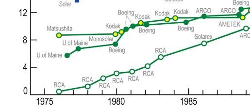
45 Chapter 2 Review of CdTe and Ge single and tandem solar cells 2.1 CdTe solar cells Cadmium telluride (CdTe) solar cells are regarded as the leading thin-film photovoltaic (PV) technology because it was the first PV technology to achieve a price per watt peak (Wp) below $1 ($0.85) in 2009, commercialized by First Solar, Inc. [43]. CdTe thin film solar cells have been studied for more than half a century, but the efficiency achieved remained at less than 20% for a long time as shown by the progress of the technology in Fig. 2.1 [43, 44]. In 2015, the solar cell efficiency of 21.5% was achieved for a research cell, and 17.5% for a module [21], thus making CdTe the leading thin film photovoltaic technology. The first single-crystal and poly-crystal CdTe solar cells were made without CdS window layers and transparent conductive oxide (TCO) contacts. In 1963, Cusano reported a CdTe solar cell that employed a p-cu 2 Te/n-CdTe heterojunction, and succeeded in obtaining 5.4% efficiency [44]. Since Cu diffusion led to instabilities in the devices, CdS was combined with CdTe to form a p-n heterojunction with efficiencies around 6% [45]. These cells were fabricated in substrate configuration, having a Mo back contact and a CdTe thickness of more than 10 μm [45]. The substrate configuration is a traditional method to fabricate semiconductor devices by stacking up materials on the bottom substrate as shown in Fig. 2.2a. The domi-


46 24 Review of CdTe and Ge single and tandem solar cells Fig. 2.1 The best efficiency of CdTe solar cells and modules. nant issues of CdTe solar cell development, such as the difficulty of doping p-type CdTe, the difficulty in obtaining low-resistance contacts to p-type CdTe, and the recombination losses associated with the junction interface became obstacles to achieve more than 6% efficiency. Ten years later in 1982, Tyan et al. [46] presented a thin film cell fabricated in superstrate configuration with more than 10% efficiency. This cell was grown by closed-space sublimation. Soon after the realization of the first CdS/CdTe device, it was recognized that a cell fabricated in superstrate configuration is more efficient. In the superstrate configuration the materials are stacked, in reverse order to that of the conventional substrate configuration, on top of a transparent support material such as glass or plastic, as shown in Fig. 2.2b. Another important milestone was the discovery that chlorine treatment (CdCl 2 ) of CdTe thin-films substantially increased device efficiency. Such optimizations resulted in laboratory scale solar cells with efficiencies exceeding 15% demonstrated by Ferekides et al. [47]. It took (a) (b) Fig. 2.2 Fabrication methods: (a) substrate, (b) superstrate configuration.
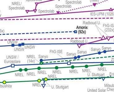
47 2.1 CdTe solar cells 25 Table 2.1 Photovoltaic properties of the best CdTe cell and module [21]. Material Eff.[%] V oc [V] I sc [A] FF CdTe cell m 79.4 CdTe module almost 10 years before the efficiency reached 16.5%, as shown in Fig The research groups at the National Renewable Energy Laboratory (NREL) and at the University of South Florida (USF) are those that pushed the efficiency to the range of 16%. It is remarkable that the highest efficiency CdTe PV devices are fabricated using polycrystalline rather than single crystalline CdTe. This is because grain boundaries enhance the collection of photogenerated minority carriers, as demonstrated by many researchers [48 50]. It is thus with great effort that the highest efficiencies at the cell and module level available to date, as shown in Table 2.1, have been made possible. Interestingly, a nontechnical challenge that CdTe technology faces is that Cd and, to a lesser extent, Te are considered as toxic materials. However, CdTe is very stable compound, which is not soluble in water and with a high melting temperature (1092 C), and once encapsulated it is definitely harmless [51] Highest efficiency First Solar, Inc. announced their highest efficiency CdTe solar cell in Although the process conditions have not been disclosed, the record solar cell performance was compared with that of other materials and with the Shockley Queisser (SQ) limit by Russell et al. [52]. The J-V curve of the record CdTe solar cell was also compared with other poly-crystalline cells and the SQ limits at standard test conditions [21]. From the results shown in Fig. 2.3, the current density of the CdTe record cell was found to be about 92% of the fundamental limit, while V oc is approaching 80% of the fundamental limit. It is noticeable that there is more room for V oc improvement. Therefore, the carrier concentration needs to be increased in the CdTe layer by overcoming dopant compensation without additional current losses to achieve higher V oc. The quantum efficiency (QE) of record cells are compared in Fig. 2.4, showing that optical losses have been largely minimized. The quantum efficiency (QE) is the ratio of the number of carriers collected by the solar cell to the number of photons given from sunlight on the solar cell. QE normally represents EQE (external quantum efficiency) including the
![26 Review of CdTe and Ge single and tandem solar cells Fig. 2.3 J-V comparison between the best efficiency record and SQ limits [52]. effect of optical losses such as transmission and reflection.](/docs-images/89/99019561/images/48-1.jpg "Internal quantum efficiency (IQE) refers to the efficiency with which photons absorbed in the cell can generate collectable carriers.")
48 26 Review of CdTe and Ge single and tandem solar cells Fig. 2.3 J-V comparison between the best efficiency record and SQ limits [52]. effect of optical losses such as transmission and reflection. Internal quantum efficiency (IQE) refers to the efficiency with which photons absorbed in the cell can generate collectable carriers. Notably, losses in the CdS window layer have been essentially eliminated, resulting in relatively square QE curves that are limited by the optical absorption of the window layers (glass/tco/cds) at short wavelengths. Optical properties of CdTe have been improved through what appears as a reduction in the bandgap of the CdTe absorber for long wavelengths [53]. It indicates that optical properties of the films were influenced by process conditions such as deposition temperature, CdCl 2 treatment and CdS-CdTe interface. Thus, the process optimization is essential to realize optimal bandgap. The effective CdTe bandgap of the cells was calculated from the 35% point of the published QE graphs, as tabulated in the legend of Fig Fig. 2.4 Quantum efficiencies of record cells [52].
49 2.2 Ge solar cells CdTe solar cells on flexible substrates One of the advantages of thin film solar cells is their potential application in flexible devices. A 16.4% high-efficiency CdTe solar cell on flexible substrates was achieved by Mahabaduge et al. in 2015 [54]. Ultra-thin glass was used as a substrate for fabrication of the flexible CdTe solar cell. The improvement was achieved by using sputtered CdS:O and coevaporated ZnTe:Cu with rapid thermal annealing. Optical properties of window materials are very important to reduce absorption losses in the window layers. Using a sputtering system, the CdS film was deposited in oxygen ambient to have high transmission in the blue region of the solar spectrum, which enhanced the short-circuit current of solar cells. As shown in Fig. 2.5 and Table 2.2, devices with sputtered CdS:O have a noticeably higher QE for shorter wavelengths than devices with the CBD CdS, resulting in the 1.2 ma/cm 2 improvement in short-circuit current density [54]. In this work, presented in Chapter 8, the thickness of the CdS film was reduced in order to achieve high transmission in the blue region of the spectrum. ZnTe:Cu was co-evaporated as a back contact in this paper, which enhanced the V oc and FF. Since Cu diffusion affects solar cell performance during heat treatment, the heat treatment after forming the back contacts with Cu should be controlled and optimized carefully. If thermal treatments during or after Cu contact formation are conducted at high temperature and/or for long process time, Cu diffusion will be induced and enhanced. Table 2.2 A comparison of flexible cells with record device parameters [54]. Material Eff.[%] V oc [mv] J sc [ma/cm 2 ] FF Old best New best Ge solar cells Ge was used for semiconductor devices and photodetectors earlier than silicon because of its high charge-carrier mobility and relatively high-absorption coefficient [55]. Furthermore, Ge is attractive for several reasons: it is a well-characterized material due to long-term research; it is an elemental semiconductor; it can be deposited and recrystallized over a wide range of temperatures, as demonstrated in the past as well as in this work. However, Ge stand-alone solar cells suffer from poor performance due to thermalization losses, a con-
50 28 Review of CdTe and Ge single and tandem solar cells Fig. 2.5 Quantum efficiencies of milestone cells on flexible substrates [54]. sequence of its relatively narrow bandgap (0.67 ev). Thus, as explained in Chapter 1, Ge is mostly used as a substrate and a bottom cell material in monolithically stacked highefficiency multi-junction solar cells developed for space applications [56]. In a tandem cell structure, if the short-circuit current of two (or more) solar cells is not exactly identical, one of the solar cells has to sacrifice its short circuit current, as shown in Fig This sacrifice limits the contribution of one of the solar cells in the tandem cell. As an alternative, a mechanically stacked solar cell in combination with a stand-alone Ge bottom cell is under development for applications in space modules and terrestrial concentrator systems (even though the top cell, in a mechanically stacked solar cell, needs to have transparent electrodes for both front and back contacts) [57]. Above all, since most research on Ge solar cells has used single crystal, which is not cost-effective, it may prove to be beneficial to study poly-crystalline Ge as a thin-film material for photovoltaic applications. Therefore, crystallization of Ge films has been studied in this thesis, and will be presented in detail in Chapter Highest efficiency For fabrication of a high-efficiency stand-alone Ge solar cells, the most important steps are forming a shallow emitter and a good passivation, because Ge has high absorption coefficient for photon energies above 0.8 ev and high surface recombination velocity at the front and rear surfaces of the cell (when unpassivated). Both thick emitter and high surface recombination will reduce the photocurrent of devices. The highest efficiency Ge solar
![2.2 Ge solar cells 29 Fig. 2.6 I-V measurement of the highest efficiency Ge solar cell [55]. cell (7.](/docs-images/89/99019561/images/51-1.jpg "8%) was obtained using an emitter formed by phosphorous diffusion from a spin-on dopant (SOD) source as shown in Fig. 2.6 [55].")
51 2.2 Ge solar cells 29 Fig. 2.6 I-V measurement of the highest efficiency Ge solar cell [55]. cell (7.8%) was obtained using an emitter formed by phosphorous diffusion from a spin-on dopant (SOD) source as shown in Fig. 2.6 [55]. Firstly, the n+ emitter was formed in a p- type Ge substrate using a spin-on dopant (SOD). Various conditions were studied to make shallow emitter as shown in Fig Subsequently, using evaporated aluminum, the back contact and the back surface field (BSF) were realized in a single process by subsequent annealing at temperatures above the Al-Ge eutectic temperature (426 C) to form a highly doped p+ zone. After isolating devices by mesa etching, a thin layer of amorphous silicon (a-si) was deposited for surface passivation. The front contact and an antireflective coating were formed by diffusion of Pd/Ag layer through this passivation layer and by evaporation of ZnS and MgF 2 respectively. From the literature, several useful methods could be adopted Fig. 2.7 Phosphorous diffusion into Ge at different temperature and time [55].

52 30 Review of CdTe and Ge single and tandem solar cells in our work. Firstly, SOD is a low-cost method to dope Ge films simply by spinning dopants and annealing. This can be applied in doping phosphorus to convert p-type poly-ge into n-type. Aluminum is a reliable candidate to form back contacts with a back surface field. As a bottom cell in a tandem cell, a Ge cell does not require passivation separately since other layers (tunnel junction) will be deposited on top of the Ge cell and metal contacts will be formed on the bottom Ge-on-glass solar cells For fabrication of Ge solar cells on a glass substrate using single-crystal Ge, epitaxial growth and wafer bonding were conducted [58]. In order to fabricate the solar cells, six steps were conducted, as schematically summarized in Fig. 2.8a : (a) growth of a Ge epilayer on a Ge substrate, (b) H-implantation, (c) wafer bonding to glass, (d) layer-splitting and chemical etch-back, (e) growth of the solar element, (f) mesa definition and contact lithography. As shown in Fig. 2.8b, the highest efficiency of 2.6% of Ge-on-glass solar cells is not as good as traditional Ge solar cells of 7.8% efficiency reported in Ref. [55]. However, it may be not directly comparable because of the different process, substrate and thickness of layers. Although epitaxial growth, wafer bonding and layer splitting are not likely to be adopted in cost-effective fabrication, they are unavoidable if glass substrates and single-crystal Ge need to be used at the same time. However, Ge deposited by simple thermal evaporation (a) (b) Fig. 2.8 (a) Fabrication of Ge on glass solar cells, (b) I-V characteristics of the highest efficiency of Ge-on-glass solar cells under AM1.5G illumination [58].
53 2.3 CdTe/Ge tandem solar cells 31 and crystallized by thermal annealing can be utilized on glass substrates without any highcost methods. Although completed Ge solar cells have not been fabricated in our work, crystallized Ge on glass substrates were investigated and Ge/Si heterojunction devices were fabricated, using solid-phase Ge crystallization, which will be presented in Chapter 4. Therefore, crystallized poly-ge provides a much simpler fabrication process at a lower cost than single crystal Ge. 2.3 CdTe/Ge tandem solar cells A CdTe/Ge tandem solar cell was proposed by Pulfrey et al. [59] to enhance CdTe solar cell performance by adding a thin-film Ge solar cell. The proposed structure is depicted in Fig As mentioned in Chapter 1 (Section 1.3), while the bandgaps of CdTe ( 1.45 ev) and of Ge ( 0.67 ev) are not optimal for a two-component tandem cell, the Ge bottom cell has the required capability of generating a photocurrent to match that of the best CdTe cells. As modeled in Chapter 8 (Section 8.2), current matching can be optimized by controlling the Ge thickness, since optical absorption is a function of thickness. The optical and electrical modeling was conducted simultaneously, and the calculated performance results are summarized in Table 2.3. CdTe/Ge tandem solar cells were modeled in detail and described by Sharp et al. [42] Fig. 2.9 A suggested structure of CdTe/Ge tandem solar cells [59]. Table 2.3 Predicted photovoltaic performance of the CdTe/Ge tandem cell in the previous work [59]. Material Eff.[%] V oc [mv] I sc [ma/cm 2 ] FF Stand-alone Ge cell CdTe/Ge tandem cell
54 32 Review of CdTe and Ge single and tandem solar cells with different thin-film CdTe/Ge tandem structures. CdTe/Ge tandem solar cell efficiencies exceeding 20% were calculated. However, a thin tunnel junction based on degenerated CdTe films, as suggested in the literature, is not realizable because dopant compensation limits the highest effective doping possible [60]. Moreover, since the efficiency of a stand-alone CdTe single cell now exceeds 20%, previous calculations may need to be revisited. Two significant factors have led to improvement in CdTe-based solar cell performance (as indicated in Subsection 2.1.1): improved optical properties of CdS films (high transmission in the blue region of the solar spectrum), and improved optical properties of CdTe films (from bandgap reduction). Optical transmission of CdS thin films was improved to allow the absorber layer to collect more photons from the blue region of the solar spectrum. Deposition conditions influence the optical properties of CdTe films, as well as their energy bandgap. Additionally, higher doping in CdTe films at the absorber or back surface field (BSF) can be employed to improve V oc. This is possibly how a high V oc was achieved in the highest record cell, which approach 80% of the fundamental limit, as shown in Fig Hence, prior performance predictions will need to be revisited, taking into account recent progress in material quality. 2.4 Summary and discussion In this chapter, research on CdTe and Ge stand-alone solar cells, and tandem cells has been reviewed. CdTe solar cells have been studied for more than half a century and have now reached an efficiency of 21.5%. The theoretical efficiency limit of around 30% for CdTe solar cells is still far from experimental results in state-of-the-art cells, but provides an optimistic motivation. While the efficiency achieved of stand-alone Ge solar cells can be further increased (e.g., employing shallow emitter region, improved surface passivation, etc.), a stand-alone Ge solar cell will always underperform CdTe cells because of thermalization losses arising from the narrow energy bandgap of Ge. However, Ge solar cells can be employed as a bottom cell in a tandem cell arrangement, either in the monolithic or the mechanically stacked configuration. CdTe/Ge tandem solar cells have been proposed a relatively simple way of improving the performance of CdTe solar cell technology. In the recent developments of CdTe solar cells ( 21.0%), improvements in QE were achieved by reducing absorption losses in the window layers and by improving the crystal quality of the CdTe layer. These two optimization strate-
55 2.4 Summary and discussion 33 gies were employed in this work. Although previously modeled CdTe/Ge tandem cells are not practical using current technology, there are opportunities for fabrication of a CdTe/Ge tandem solar cells, as predicted by realistic simulations presented in Chapter 8.
56
57 Chapter 3 Experimental and characterization techniques There are various methods to deposit films for the fabrication of thin film solar cells. The properties of the deposited thin films have been found to depend both on deposition method and deposition conditions [61, 62]. Chemical-bath deposition (CBD) and close-spaced sublimation (CSS) are arguably the most popular techniques for the preparation of CdS and CdTe thin films, respectively, due to the high quality of the films produced and their high throughput [63]. For Ge films, different deposition techniques and recrystallization methods have been utilized by many researchers [64]. In this work, evaporation techniques were employed to fabricate solar cells, since these are relatively low-cost and low-temperature processes that can be employed for all relevant materials (CdS, CdTe and Ge). The thermal evaporation method was employed to deposit, and fabricate CdS and CdTe solar cells, on bare glass or ITO-coated glass substrates; whereas for poly-ge films, e-beam evaporation and furnace annealing were employed for the deposition and solid phase crystallization (SPC), respectively. Furthermore, the material properties and fabrication process that impact the performance parameters of thin-film solar cell need to be investigated. This demands the deployment of various characterization techniques to gain insights that will enable optimization of material characteristics and device performance. In this work, the required investigation of structural,
58 36 Experimental and characterization techniques optical and electronic properties of evaporated Ge, CdS and CdTe was conducted. For the characterization of electronic properties, Hall effect, current-voltage (I-V), and capacitancevoltage (C-V) measurements were employed. I-V measurement in the dark and/or under illumination were employed for the characterization of parasitic effects, and to identify loss mechanisms and to quantify fundamental device properties. Structural characterization relied on X-ray diffraction (XRD) and scanning electron microscopy (SEM) to investigate the crystallinity, and the surface and cross-sectional morphology of deposited thin films. Optical characterization required the use of transmission, absorption and reflection spectroscopy to evaluate optical properties of thin films. Scanning laser microscopy (SLM) was employed to evaluate spatial photocurrent distribution in heterojunction devices. Optical property parameters, such as refractive index and extinction coefficient, were extracted from the measured characteristics to enable the modeling of thin film solar cells on the basis of experimentally determined parameters. All deposition, annealing and device fabrication processes were conducted at the University of Western Australian (UWA), employing facilities supported by Australian National Fabrication Facility (ANFF). 3.1 Review of deposition methods Ge deposition techniques Single-crystal Ge ingots and wafers are produced via the Czochralski process, and homoepitaxial and heteroepitaxial Ge layers can be deposited using various epitaxy methods. Homoepitaxial Ge layers have been grown by means of metal organic vapor phase epitaxy (MOVPE) using iso-butyl germane (ibuge) as metal-organic precursor [65]. Heteroepitaxial Ge layers have been grown selectively on silicon substrates patterned using a SiO 2 mask for the realization of pmosfets [66]. However, despite the demand for Ge films for applications such as tandem solar cells, these growth methods are not likely to be utilized for the realization of a commercially viable Ge-based photovoltaic technology, due to their high cost and low throughput. In this subsection, methods for the preparation of polycrystalline Ge (poly-ge) thin films on low-cost substrates, such as glass, were investigated to provide scope for a low-cost fabrication process for optoelectronic device applications, especially monolithic tandem solar cells.
59 3.1 Review of deposition methods 37 In the realisation of high-quality poly-ge thin films, post-deposition recrystallization appears to have greater impact on crystal quality than the deposition method. The recrystallization process step is performed by thermal annealing after deposition of amorphous germanium (a-ge). Many studies have reported investigations of solid-phase crystallization (SPC) in germanium thin films deposited and crystallized using various methods and techniques, with most studies seeking to optimize optical and electrical properties of the material for specific applications [67 74]. Generally, solid-phase crystallization (SPC) is a simple and cost-effective method to crystallize amorphous materials deposited on substrate materials such as glass [75]. The thermodynamics and kinetics of solid-phase crystallization from the amorphous phase to the poly-crystalline phase can be explained employing classical nucleation and growth theory, as depicted schematically in Fig When amorphous films are annealed to a certain temperature, the film is transformed into a thermodynamically stable crystalline phase through four steps: incubation, nucleation, growth, and steady state. In this process, small crystallites are formed at nucleation sites, which then grow in size with increasing time at the expense of the contiguous amorphous matrix [76]. Solid-phase epi- Fig. 3.1 Schematic illustration of solid phase crystallization processes in a-si: (a) random nucleation and growth, (b) solid phase epitaxy [76].
60 38 Experimental and characterization techniques taxy (SPE) growth, in contrast, can be regarded as an interface mediated process, since the rearrangement of atoms is influenced by the interface between the amorphous film and the single-crystal template [77], as shown in Fig In order to achieve lower costs and utilization in a wider range of applications, inexpensive materials such as glass are more attractive than quartz substrates. For the case of glass substrates, material and device processing steps need to be limited to temperatures below 550 C. In this case, simple SPC of Ge films is a feasible process for the realization of poly-ge because a-ge films start to crystallize at around 400 C, as described in Chapter 4. An alternative technique is rapid thermal annealing (RTA), which has the advantage of high heating rates (up to 60 C/s) that result in significant reduction of the total crystallization time. During RTA, thermal radiation is applied in pulses to heat the sample surface, minimizing heating of the glass substrate (which is transparent to the infrared radiation). In an effort to reduce the crystallization temperature and crystallization time, and to increase the grain size, metal-induced crystallization (MIC) has also been investigated as an alternative crystallization process for thin-film device fabrication. MIC is in general an interface-controlled phenomenon occurring in metal/amorphous semiconductor systems. Initially the interfacial covalent bond weakening effect, in the interface between the semiconductor and metals, generates a limited amount of high mobility semiconductor atoms. These free semiconductor atoms may migrate along short-circuit fast diffusion paths such as metal/semiconductor interfaces and metal GBs at low temperatures. The occurrence of intermediate wetting, the nucleation of crystallization, and the continued semiconductor crystal growth are all governed by the interface thermodynamics under the constraint of a limited amount of available free semiconductor atoms [70, 78 81]. The Ge MIC process involves the deposition of a-ge films on top of which a layer of suitable metal is deposited. This bilayer of metal and Ge is then annealed in a furnace at temperatures ranging from 150 to 500 C for durations between one minute to several hours, leading to crystallization of the a-ge. The growth rate depends on the annealing conditions of the bilayer. In the MIC process, metals such as aluminum, nickel, gold, etc. are used to decrease the crystallization temperature below 500 C, as shown in Fig 3.2. In case of Pd and Cu, it has been reported that crystallization starts at a low temperature of around 300 C. However, the metals required for MIC tend to contaminate poly-ge and thus degrade its properties. The investigation of metals that would enable crystallization of a-ge thin film at
61 3.1 Review of deposition methods 39 Fig. 3.2 Phase diagram describing crystal status of 200 nm thick undoped Ge films processed by MIC technique with Pd, Cu, Ni, Au, Co, Al, Pt, and Tifor1hatseveral temperatures between 300 and 450 C [70]. Table 3.1 Summary of Ge crystallization using a variety of techniques. Reference Experimental condition Deposition Substrate Toko et al. [69] Watakabe et al. [71] Park et al. [70] Tsao et al. [68] Tsao et al. [82] Kobayashi et al. [83] Two-step annealing at 425 C for 500min and at 500 C Pulsed laser annealing with boron implant doping Metal induced crystallization(mic) with various metals at different temperature Sputtered at low substrate temperature( C) and SPC annealed at high temperature( C) Sputtered at substrate temperature of 450 C Annealing at 900 C for 30min with SiO 2 capping layer Deposited at 600 C Molecular beam deposition Sputtering Deposited Ge films at 300 C using LPCVD RF Magnetron Sputter RF Magnetron Sputter Evaporation Quartz Quartz SiO 2 grown on a Si wafer Si 3 N 4 coated glass Si 3 N 4 coated glass Si 3 N 4 coated Si low temperatures, with minimal contamination, is an area of continuing research. A variety of techniques have been reported in the literature that have achieved highquality poly-ge thin films, as summarized in Table 3.1. Some of the techniques employed still need to be optimized in terms of temperature and process times to enable their use in the fabrication of cost-effective solar cells. Interestingly, a SiO 2 capping layer was suggested to prevent Ge re-evaporation loss during SPC at high temperature [69, 83]. More importantly,

62 40 Experimental and characterization techniques Fig. 3.3 Operation of electron beam evaporation. it was found that the temperature for Ge crystallization is sufficiently low to be used with low-cost substrates. An attractive technique is electron beam (ebeam) evaporation, which is commonly used to produce thin films and metallization layer. It is a relatively simple technique which have a minimal number of controlling parameters, as shown in the schematic diagram in Fig When filament is heated by controlled current flow, thermionic emission of electrons takes place. The electrons are focused and directed toward the material source by a magnetic field. The evaporation is performed using the electron beam that scans the surface of the evaporation source and evaporates or sublimates the material at the surface, without fully melting the source material in the crucible. In his way the impurities located in the crucible do not diffuse and contaminate the very pure evaporation source material CdS deposition techniques As a wide bandgap material (Eg=2.42 ev at 300 K), CdS is largely transparent down to wavelengths of around 520 nm, which is why CdS films are very attractive as a window layer in thin film solar cells. CdS can be deposited by various techniques such as vacuum evaporation (physical vapor deposition) [84, 85], close-spaced sublimation (CSS) [86], chemical bath deposition (CBD) [87], sputtering [88, 89], etc. In CdS/CdTe thin-film solar cells, CdS layers deposited by low-temperature techniques generally require a post-deposition annealing treatment for recrystallization prior to the deposition of the CdTe absorber layer. The
63 3.1 Review of deposition methods 41 structural and optical properties of CdS layers are strongly dependent on the deposition technique (deposition mechanism and conditions), so the properties must be matched with the characteristics of the CdTe absorber layer. Two techniques, sputtering and chemical bath deposition (CBD), recently utilized in research and manufacturing, are reviewed below. Sputtering Sputtering is a physical deposition process whereby atoms/molecules are ejected from a solid target material by bombardments with energetic particles. When using a plasma, an inert gas (usually argon) is introduced at low pressure into the vacuum chamber where the substrate and the source material are placed. The gas is ionized using an RF power source. The accelerated ions move towards the surface of the target and cause the ejection of material from the source in vapor form, which then condenses on the substrate to form a thin film layer [90]. Sputtering has significant advantages in use of low energy particle bombardment which results in lower substrate temperatures during deposition. Forming gas and co-sputtering have also been used to improve doping control during growth [91, 92]. The sputtering method has been employed by many researchers for the preparation of CdS thin films, and has also been employed in the mass production of large-area modules [88, 93 95]. The electrical and optical properties of sputter-deposited CdS thin films vary with the annealing temperature, which tends to control phase composition, grain-size, and stoichiometry of the CdS thin films. As shown in Table 3.2, the optical bandgap of CdS films sputtered at room temperature is narrower than the ideal bandgap. Post-deposition annealing, or substrate heating during deposition, is often necessary to improve optical properties. Sputtered oxygenated cadmium sulfide (CdS:O) has optical properties that result in improved solar cell absorption in the blue region of the sun spectrum, as a consequence of increase of the energy bandgap in CdS:O films [93, 96 99]. The improved quantum efficiency of sputtered oxygenated cadmium sulfide (CdS:O) has already been reviewed in Chapter 2 (Section 2.1). Chemical bath deposition The chemical bath deposition (CBD) technique produces uniform thin films at a relatively low cost with technical simplicity. This deposition method yields stable and reproducible CdS films with good adhesion and consistent properties [100]. CBD CdS films
64 42 Experimental and characterization techniques Table 3.2 Optical bandgap of sputtered CdS films. Reference Optical bandgap Deposition Substrate Liang et al. [88] Kim et al. [95] Lisco et al. [94] Meysing et al. [93] 2.32eV(Room temp.)/ 2.37eV(Annealing at 100 C) 2.41eV(Room Temp.)/ 2.43eV(Annealing at 400 C) 2.31eV(Room Temp.) 2.8eV Ion-beam sputtering RF sputtering Pulsed DC magnetron sputtering Reactive sputtering in the oxigen ambient Glass ITO-coated Corning glass FTO coated glass - contain a high concentration of oxygen, which is responsible for their high n-doping and low sheet resistance [101]. High n-doping in the CdS layer should result in a high built-in potential across the CdS/CdTe junction, and consequently lead to a high photovoltage [102]. However, CBD CdS films tend to form a cubic phase and have poor crystalline quality, which makes post-deposition annealing necessary to improve their optical and electric properties. CdS films grown by CBD rely on the decomposition of thiourea (CS(NH 2 ) 2 ) in the presence of a cadmium salt in a basic solution, with ammonia as a complexing agent. The formation of tetra-amino-cadmium complex ions, [Cd(NH 3 ) 4 ] 2+, is important for the liberation of Cd 2+ ions that then recombine with S 2 ions to produce CdS. The chemical reactions that yield CdS films are as follows [87]: Cd OH Cd(OH) 2 (3.1) NH OH NH 3 + H 2 O (3.2) Cd(OH) 2 + 4NH 3 [Cd(NH 3 ) 4 ] OH (3.3) CS(NH 2 ) 2 + 2OH S 2 +CN 2 H 2 + 2H 2 O (3.4) [Cd(NH 3 ) 4 ] 2+ + S 2 CdS(s)+4NH 3 (3.5) The chemical reaction is accelerated by heating the chemical bath. The process results in CdS deposition on the surface of sample substrates and also on the inner reactor walls. The deposition rate can be modulated by controlling the bath temperature, the chemical reagent concentrations and the agitation of the bath during deposition [87, 103, 104]. A required film thickness can be obtained with either single and/or multiple immersion of a substrate in
 thin films were deposited using several techniques to compare their properties; chemical bath deposition (CBD) vs.")
65 3.1 Review of deposition methods 43 the solution. However, CBD is a relatively slow process that results in high liquid wastage which demands recycling. CdS deposition techniques used in this work Cadmium sulfide (CdS) thin films were deposited using several techniques to compare their properties; chemical bath deposition (CBD) vs. vacuum evaporation (VE) [62], closespaced sublimation (CSS) vs. RF magnetron sputtering [105], and close-spaced sublimation (CSS) vs. chemical bath deposition (CBD) [106]. A direct comparison was not sufficient to determine which technique is appropriate, since the CdS film properties were not assessed from the viewpoint of device performance. Although deposition conditions (temperatures and process times) and film properties (optical, morphological and electrical) were compared, there was no systematic investigation of the thier effect on device characteristics and performance. Although the optical and electrical properties of evaporated CdS thin films have been found to be superior to those deposited by chemical bath deposition (CBD), the photovoltaic properties of solar cells with evaporated CdS are inferior to those with CBD CdS [62]. Post-deposition processes, such as CdTe deposition and CdCl 2 treatment, may need to be optimized for a particular CdS deposition process, since CdS films deposited by different techniques tend to have significantly different film properties. In this work, thermal evaporation was employed to deposit CdS thin films, since it is a method amenable for large-area deposition of thin films required for solar cell applications, as depicted in Fig Thermal evaporation techniques, with the required temperature con- Fig. 3.4 Operation of thermal evaporation.
66 44 Experimental and characterization techniques trol, are easily scalable and well developed in the semiconductor industry. Hence, the process is attractive for simple in-line deposition of large-area CdTe solar modules on soda-lime glass substrates, as well as on polymer foils for flexible solar modules [107] CdTe deposition techniques Numerous methods have been employed to deposit CdTe thin films for solar cells in the past. Fig. 3.5 presents a schematic diagram of each fabrication procedure, including process temperature and pressure conditions, film thickness, and growth rate. All have led to good cells exhibiting efficiencies above 10%, although only a few processes have properties suited to large-scale production [61]. Close-spaced sublimation (CSS) The Growth of high quality CdTe is facilitated by the ability to deposit on substrates held at elevated temperatures [52, 54, 61]. However, re-evaporation of Cd and Te from the growing CdTe surface due to the high temperature of the substrate limits the deposition rate and utilization. Thus, the source and substrate need to be in close proximity, and the CSS method was designed to achieve that. For close-spaced sublimation (CSS), the CdTe source material is supported in a holder facing the substrate in the same area. The space between source and substrate allows thermal isolation, so that a temperature differential can be sustained throughout the duration of the deposition. The ambient for deposition typically contains a nonreactive gas such as N 2, Ar, or He. A small partial pressure of O 2 appears to be crucial for obtaining good film density and solar cell junction quality. As-deposited CSS films deposited above 550 C exhibit large grain size that is comparable to film thickness. The CSS process has been intensively investigated by many researchers and has yielded the highest cell performance. Vapor transport deposition (VTD) As-deposited vapor transport deposition (VTD) yields films that are similar to those obtained by CSS, because of the similarity in deposition conditions [61, ]. VTD allows high-rate deposition at high substrate temperature, at pressures approaching 0.1 atm onto moving substrates. VTD works by transferring a vapor stream saturated with Cd and Te to the substrate, where extreme saturation of the Cd and Te vapors results in condensation
67 3.1 Review of deposition methods 45 and reaction to form CdTe. The CdTe source is exhausted from a heated chamber containing solid CdTe in which the carrier gas mixes with the Cd and Te vapors through a slit over or under the moving substrate at a distance on the order of 1 cm. The carrier-gas composition can be varied, as with CSS. Close space sublimation (~10 Torr) 600 C Vapor transport deposition ( Torr) Carrier gas CdTe 700 C CdTe C 600 C d = μm/min d = μm/min Physical vapor deposition Cd + Te 2 vapor Solid CdTe (10 6 Torr) 400 C C d = μm/min Electrodeposition + (1 atm) Sputter deposition (10 4 Torr) 200 C CdTe target d = 1 4 ~0.1 μm/min Metal organic chemical vapor deposition Source gases (1 atm) Cd ++ HTeo C C d = μm/min Spray deposition CdCl 2 + Te (1 atm) d = μm/min Screen print deposition (1 atm) CdTe slurry Screen 600 C d = 1 20 ~1 μm/min d = 5 30 μm ~ 25 C Fig. 3.5 Schematic diagram of various techniques for CdTe thin film deposition [61].
68 46 Experimental and characterization techniques Sputter deposition CdTe films have been deposited by radio-frequency magnetron sputtering from compound targets [61, 89, 111, 112]. Mass transfer of Cd and Te occurs via ablation of the CdTe target by Ar + bombardments. Typically, deposition is carried out at a substrate temperature of less than 300 C and at pressures of 10 mtorr. As-deposited films deposited at 200 C exhibit grain diameter < 300 nm. For CdTe cells prepared by close-spaced sublimation, a temperature of C is used, whereas cells deposited using sputtering are prepared at 370 C or below. For industrial applications it would be beneficial if the materials for high performance solar cells could be deposited at lower substrate temperatures of 400 Ctouse low-cost substrates such as glass. Spray deposition Spray deposition is a solution-based and nonvacuum technique with a slurry containing CdTe, CdCl 2, and a carrier such as propylene glycol [61, ]. The slurry can be sprayed onto unheated or heated substrates followed by a reaction/recrystallization treatment. In this process, the mixture is sprayed onto the substrates at room temperature and baked at 200 C, followed by a bake in the presence of O 2 at 350 to 550 C, a mechanical densification step, and a final treatment at 550 C. Films produced by spray deposition vary in morphology, grain size, and porosity, but films used to make high-efficiency cells have been found to exhibit a 1 to 2 μm-thick dense region near the CdTe-CdS interface and a relatively porous back surface region. A distinction of the fabrication process was the consumption of the CdS layer, forming a nearly uniform CdTe 1 x S x alloy. Screen-print deposition (roll-to-roll screen printing) Screen-print deposition is a simple technique with a paste containing Cd, Te, CdCl 2, and a suitable binder [61, 117, 118]. That is applied to the substrate through a screen. Following a baking step to remove binder solvents, the layer is annealed at temperatures up to 700 C to recrystallize the film and activate the junction. Films fabricated by this method typically have a thickness ranging from 10 to 20 μm with lateral grain dimension of 5 μm. Due to porosity, comparatively thick layers are required for good operation of the cells.
69 3.2 Substrate preparation 47 CdTe deposition technique used in this work In this work, a simple thermal evaporation technique was employed to deposit CdTe thin films as shown in the schematic diagram in Fig 3.4. The advantage of this technique for CdTe films is the relatively low substrate temperature required, and the stable properties of the deposited film which exhibit no pinholes. The substrate temperature required is low enough to be used for glass or flexible substrates. Furthermore, CdS films can also be deposited in the same chamber without breaking vacuum. Since CdTe can be deposited by coevaporation from elemental sources or by direct sublimation from a CdTe source in separate crucibles, the stoichiometry of the CdTe can be controlled through different evaporation rates and substrate temperature [119]. For deposition in moderate vacuum, 10 6 Torr, at a source to substrate distance of 19 cm, a deposition rate of 42 nm/min was achieved on substrates at 330 C. At higher substrate temperatures, the sticking coefficients of Cd and Te decrease, resulting in a lower effective deposition rate, imposing a practical upper limit to substrate temperature of approximately 400 C, which is still compatible with low-cost substrates [119]. 3.2 Substrate preparation Several types of substrates, such as glass microscope slides, ITO (indium tin oxide) coated glass, and single-crystal silicon wafers were employed for the experiments. Glass microscope slides were used for analyzing thin film properties on a transparent insulating substrate for Hall measurement, optical transmittance, and XRD. Silicon wafers were utilized to fabricate and analyze the crystallization of Ge films on Si substrates, and for p-ge/n-si and n-cds/p-si heterojunction devices. Commercial ITO-coated glass substrates were used for CdTe solar cells fabricated in superstrate configuration. Specifics of the substrates are tabulated in Table 3.3, and optical properties (transmission, absorption and reflectance) of the substrates were measured and are depicted in Fig Table 3.3 Specifics of various substrates. Thickness Resistivity Dopant Orientation Glass microscope slides 1 mm Insulator - - ITO-coated glass 180nm ITO film 9-15ohm/sq - - n-type Si 350 μm 1-10ohm-cm Phosphorous (100) p-type Si 640 μm ohm-cm Boron (100)
70 48 Experimental and characterization techniques Fig. 3.6 Measured optical properties (transmission, absorption and reflectance) of various substrates with 200nm evaporated CdS film. Initially in the fabrication process, cleaning of substrates is essential to remove any dust and surface contamination that may affect the performance of devices and properties of the deposited materials. All substrates were cleaned by consecutive baths of acetone, methanol and isopropyl alcohol (IPA), and then washed in warm deionized water in an ultrasonic cleaner. For silicon substrates, additional HF etching was performed to remove any native oxide by dipping in 30% diluted HF for a few seconds after conventional solvent cleaning, and prior to thin film deposition. ITO-coated glass substrates were annealed at 500 C for 10 min in a furnace with flowing N 2 to prevent film delamination between ITO and CdS, which was observed during the high temperature CdCl 2 anneal. 3.3 Structural characterization X-Ray Diffraction (XRD) XRD, which is a non-destructive technique, is used to identify the structure and phases of a material. The scattering centers for x-rays rely on the fact that crystals are composed of regularly spaced atoms. X-ray waves interact with the atoms in a crystal, and diffraction will
71 3.3 Structural characterization 49 occur if the wavelength of the x-ray and the atomic spacing of the crystal are comparable, as shown in Fig If θ is the angle at which the x-rays enter a crystal relative to one of the atomic planes, and 2a is the path difference between the two rays, then 2d sinθ = nλ (3.6) where n is an integer, λ is the wavelength of x-rays incident on the crystal and d is the distance between lattice planes. Equation 3.6 is known as Bragg s Law for x-ray diffraction. A strongly diffracted beam occurs if the rays scattered by all the atoms in the planes interfere constructively and are in phase. Furthermore, constructive interference would fail if the scattering atoms were not arranged in a regular periodic manner, since the scattered rays would have random phase [120]. The diffraction peaks are analyzed to determine the d hkl spacing of the plane causing that peak. The characteristics of the unit cells of each phase present in the material can be determined from the intensity and position of the peaks. ( ) λ 2 = sin2 θ 2a h 2 + k 2 + l 2 (3.7) This equation predicts, for a particular incident wavelength λ and a particular cubic crystal of unit cell size a, all the possible Bragg angles at which diffraction can occur from the planes(hkl) [121]. The XRD system used in this work is an Empyrean multi-purpose XRD produced by PANalytical and located at the center for microscopy, characterization and analysis (CMCA) at UWA. The radiation is Copper K alpha and the instrument is equipped with a wide range of collimators, monochromators, detector systems and a high precision, multi-purpose, 5 axis Fig. 3.7 X-ray diffraction.
72 50 Experimental and characterization techniques sample stage. For thin film analysis, a 2θ scan with a fixed grazing angle of incidence and 5 axis stage was used in order to avoid any intense signal from the substrate and to obtain a stronger signal from the film itself Scanning Electron Microscopy (SEM) SEM studies were carried out to investigate the surface morphology. A scanning electron microscope consists of an electron gun and a series of electromagnetic lenses and apertures. The electron beam emitted from the electron gun is condensed to a fine probe for surface scanning. The electron gun for generating an electron beam is either thermionic or field emission type. Advanced SEM systems use a field emission gun because of its high beam brightness. A vacuum is required in order to avoid scattering and absorption. Several interactions take place when the electron beam is focused on the sample surface and what is emitted from the surface is detected by a suitable detector. When high-energy electrons strike a specimen, they produce either elastic or inelastic scattering. Elastic scattering produces backscattered electrons (BSEs), which are incident electrons scattered by atoms in the specimen. Inelastic scattering produces secondary electrons (SEs), which are electrons ejected from atoms in the specimen. BSEs are typically deflected from the specimen at large angles and with little energy loss; they typically retain 60 80% of the energy of incident electrons. In contrast, SEs are typically deflected at small angles and show considerably low energy compared with incident electrons. In terms of usefulness, SEs are the primary signals for achieving topographic contrast, while BSEs are useful for information of elemental composition contrast [120]. In order to observe the thin film surface clearly, short working distance and low acceleration voltage during operation are required, as shown in Fig The SEM (model: Zeiss 1555 VP-FESEM) in this work is a high resolution, fieldemission variable-pressure (VP) scanning electron microscope (SEM) located at the center for microscopy, characterization and analysis (CMCA) at UWA. The instrument can operate in normal high-vacuum SEM mode or in variable-pressure mode (VPSEM) with a chamber gas (usually air) pressure up to 130 Pa, and at low temperature (cryosem). To see the cross-section of samples clearly, carbon tape and silver epoxy were used to mount the samples on a sample holder without metal coating because charging effect is not serious.
![3.4 Electrical characterization 51 Fig. 3.8 Crystallized Ge surface image by SEM with short working distance (7.5mm) and low acceleration voltage (3keV). 3.4 Electrical characterization 3.4.1 Hall effect Hall effect measurement has been a well-known tool for material electrical characterization since Edwin Hall discovered the phenomenon in 1879 [122].](/docs-images/89/99019561/images/73-0.jpg "When a semiconductor with a current I x is placed in a magnetic field perpendicular to the current flow direction, electrons and holes flowing in the semiconductor will experience a force due to the")
73 3.4 Electrical characterization 51 Fig. 3.8 Crystallized Ge surface image by SEM with short working distance (7.5mm) and low acceleration voltage (3keV). 3.4 Electrical characterization Hall effect Hall effect measurement has been a well-known tool for material electrical characterization since Edwin Hall discovered the phenomenon in 1879 [122]. When a semiconductor with a current I x is placed in a magnetic field perpendicular to the current flow direction, electrons and holes flowing in the semiconductor will experience a force due to the magnetic field. In a p-type semiconductor, there will be a buildup of positive charge on the y=0 surface of the semiconductor and, in an n-type semiconductor, there will be a buildup of negative charge (see Fig. 3.9). This net charge induces an electric field in the y-direction that counters the Lorentz force exerted by the magnetic field. The induced electric field in the y-direction is called the Hall field (E H ). The Hall field produces a voltage across the semiconductor which is called the Hall voltage (V H ). A Hall effect measurement system is useful for determining various material parameters. Carrier mobility, carrier concentration, Hall coefficient (R H ), resistivity, magnetoresistance (R B ), and the carrier conductivity type (N or P) can all be derived from Hall measurements [28, 122]. Van der Pauw method The Van der Pauw method is one of the most utilized measurement methods for the evaluation of electrical properties in semiconductor materials, such as resistivity. The Van der

74 52 Experimental and characterization techniques Fig. 3.9 Geometry for measuring the Hall effect. Pauw method can be used to measure samples of arbitrary shape, although several basic sample conditions must be satisfied to obtain accurate measurements, such as the thickness of the sample must be constant, point contacts placed at the edges of the samples must be used for the measurements, and the sample quality has to be homogeneous. Most semiconductor samples satisfy these conditions, so that this convenient measurement method has been widely utilized. In the Van der Pauw method as shown by schematic diagrams in Fig. 3.10, resistivity ρ can be calculated using Eq.3.8 and Eq exp( πr v /R s )+exp( πr h /R s )=1 (3.8) ρ = R s d (3.9) where R v is a resistance measured from the y direction of the sample (R BC,DA ), R h is a resistance measured from the x direction of the sample (R AB,CD ), R s is a sheet resistance and (a) (b) Fig Schematic diagrams of (a) resistivity and (b) Hall effect measurements by the van der Pauw method.
75 3.4 Electrical characterization 53 d is the thickness of the sample. From the Hall equation 3.10, carrier concentration can be extracted. n = IB qv H d (3.10) n s = IB qv H (3.11) where n is carrier concentration, I is current, B is magnetic field and V H is Hall voltage. μ = 1 qn s R s (3.12) Carrier mobility can be extracted using Eq.3.12 based on an assumption that there is one carrier type with a discrete mobility. Measurement system Hall effect measurements were performed using a 2T electromagnet setup located at the University of Western Australia, as shown in Fig The equipment is capable of producing magnetic fields ranging from -2 Tesla to +2 Tesla using an Oxford instruments electromagnet and controlling the sample temperature between 90K and 350K using liquid nitrogen. The sample holder is placed between the poles of the electromagnet. The sample is also provided with connections to a Hall card which is a switching matrix which connects the appropriate sample contacts to the current source/voltmeter in order to perform the measurement. The current source, ammeter, Hall card and magnet power supply are all connected to a computer through an IEEE-488 Bus controller. The Keithley current source and voltmeter are digitally controlled by the computer. The switching box is connected to a digital control card which allows the computer to connect the voltmeter and current source to the appropriate contacts on the sample. The computer also has a digital to analog converter installed, which enables it to control the electromagnet Current-voltage (I-V) I-V measurements are one of the most important techniques used to obtain information on the electrical properties of fully fabricated devices. A device is said to be ohmic (non-active) or rectifying (active) from the shape of the I-V characteristics, which can be

76 54 Experimental and characterization techniques Fig The 2T Hall effect measurement setup. measured either in the dark or under illumination. All measurements were conducted using a probe station in a dark box, and either a HP4156B or a HP4145B semiconductor parameter analyzer. I-V characteristics in the dark The ideality factor n is a constant used to describe the simple exponential dependency in the current-voltage characteristics of a semiconductor junction as ( ) ] eva I = I s [exp 1 nkt (3.13) where I s is the saturation current, V a is the applied bias, k is Boltzmann s constant, T is temperature and e is electronic charge. When n equals 1, it is an ideal junction since it follows the well-known diffusion current diode mechanism. The ideality factor is a useful parameter since it can be used to identify for diode current mechanism and thus determine device quality. For example, in a simple p-n junction diode, the diffusion current component in the quasi-neutral region has an ideality of 1, while the generation-recombination current component through mid-gap trap levels in the depletion region has an ideality factor of 2 [28]. As shown in Fig. 3.12, the ideality factor can be obtained from the slope of the semilog-
77 3.4 Electrical characterization 55 Fig Extraction of ideality factor with modeling. arithmic plot of the forward current as a function of voltage, i.e. the ln(i)-v plot, thus : n = e dv a kt dlni (3.14) The ideality factor extracted by fitting I-V curves from fabricated Ge/Si heterojunctions is 1.5, as shown in Fig When ideality factor is 1 or 2, the expected plots were modeled and depicted in Fig (dot lines) using several parameters such as I s and R s extracted from the experimental plot. Series resistance (R s ) and shunt resistance (R sh ) are the two parasitic factors affecting diode current, as shown in Eq These parameters have a significant effect on the photovoltaic properties, mainly FF. ( e ) ] I = I 0 [exp nkt (V a R s I) 1 + V a (3.15) R sh These parameters can be deduced from the I-V curve in the dark or under illumination. For optimum efficiency, R s must be minimized and R sh must be maximized in order to improve the FF. These two resistances play crucial roles as follows: 1. In the ideal situation, R sh should tend to infinity (or be finite but very large), which implies very low leakage current (dark current). In a practical device, this is not the case, since defect levels/recombination centers reduce the value of R sh within the cell. Thus, the current has an alternative lower resistive path through which to flow (i.e.
78 56 Experimental and characterization techniques (a) (b) Fig Extraction of parasitic resistances (R s and R sh ) under illumination ((a) Diode shunt resistance R sh extracted in reverse bias, and (b) Diode series resistance R s extracted in forward bias). leakage current). The gradient of the I-V curve in the reverse direction can be used to extract the value of R sh as shown in Fig. 3.13a. 2. R s should be zero in an ideal situation, and it represents the total resistance of the bulk semiconductor, contact metallization and their interconnection. The R s can be extracted from the forward direction of the I-V curve gradient at high current densities as shown in Fig. 3.13b. I-V characteristics under illumination Four important solar cell parameters can be deduced from the I-V characteristic under illumination, as shown in Fig. 3.14, which includes: 1. Open-circuit voltage (V oc ): This is the voltage obtained when the terminals are open circuit and no current is flowing in the external circuit. The V oc can be increased by increasing the junction barrier height and doping concentrations, minimizing defects, and reducing the temperature of the cell. 2. Short-circuit current density (J sc ): This parameter can be obtained when the external terminals are short-circuited, in which case the potential drop across the sample will be zero. J sc can be increased by reducing the density of grain boundaries, increasing charge carrier mobility (μ), maximizing absorption of solar radiation, increasing the internal electric field, reducing recombination and generation mechanisms, separating electron-hole pairs more efficiently and using graded bandgap devices.
79 3.4 Electrical characterization 57 Fig Photovoltaic I-V curve under illumination. 3. Fill factor (FF): This parameter is related to the power conversion efficiency of the cell relative to an ideal cell (see Fig. 1.8). Several parameters such as parasitic resistance affect solar cell performance by reducing maximum power generation. Fig shows parasitic resistance (R s and R sh ) effect on fill factor in I-V curve of solar cells. The FF can also be increased by increasing the internal electric field and minimizing defects present in the device structure. The detailed calculation of FF was introduced in Chapter 1 (Subsection 1.2.1). 4. Efficiency (η): Solar cell efficiency is the ratio of the electrical energy output of a solar cell relative to the incident energy in the form of sunlight. The energy conversion efficiency (η) of a solar cell is the percentage of the solar energy to which the cell is exposed that is converted into electrical energy. The detailed calculation of η has been introduced in Chapter 1 (Subsection 1.2.1) Capacitance-voltage (C-V) The measurement technique that is used to extract doping concentration (N d ) of the semiconductor and the diffusion capacitance of the diode is capacitance-voltage measurements at high frequency. The junction depletion width (w) and the barrier height (φ b ) can also be determined. A high frequency AC signal of 1 MHz is used as the modulation frequency for the measurement. The junction is probed by the AC signal which modulates free carriers on both sides of the junction and thus the depletion region associated with the device. A graph
80 58 Experimental and characterization techniques Fig A typical graph of 1/C 2 versus voltage (e.g. Si/Ge heterojunction diode). of 1/C 2 versus V gives a straight line for a one-sided abrupt junction, from which the builtin voltage (V bi ) can be determined from the intercept on the V-axis as shown in Fig A straight line graph is obtained if the material is uniformly doped, and its gradient gives the doping concentration using: ( ) 1 2 C = 2(V bi +V R ) (3.16) eε s N d if N a >> N d where, V bi is the built-in potential, ε s is the permittivity of the semiconductor, and other symbols have their usual meanings. However, generally it is difficult to obtain a straight line in compound semiconductors such as GaAs and CdTe. C-V measurements were performed using a HP 4280A capacitance meter. Open and short corrections were always performed before measurements to obtain precise capacitance. Samples were measured employing a 30mVrms signal at 1 MHz in a probe station enclosed in a light-tight dark box. 3.5 Optical characterization Spectroscopy for optical properties Spectroscopy was carried out to evaluate thin-film optical properties, such as transmission, absorption, and reflection, as well as to extract the bandgap of the semiconductor material. The optical energy bandgap of samples was deduced from the intercept of the extrap-
81 3.5 Optical characterization 59 olated linear part of the plot of (αe) 2 vs the photon energy E. This follows the method of Tauc et al. [123]: α = B(E E g) 1 2 E (3.17) where α is the absorption coefficient, E is the photon energy, and B is a factor that depends on the transition probability and can be assumed to be constant within the optical frequency range [95, 124, 125]. The optical absorption coefficients of samples are evaluated from the transmittance data using [95]: [ α = 1 ] d ln (1 R) 2 (1 R) 4 + 2T 4T 2 + R 2 (3.18) where T is the transmittance, R is reflectance, α is the absorption coefficient, and d is the thickness of the film. The measurements were conducted using a spectroscope model F10-RT produced by Filmetrics Inc. installed in the cleanroom in the University of Western Australian, the WA node of the Australian National Fabrication Facility (ANFF). The instrument uses a light source having wavelengths between 380 and 1050 nm. This instrument measures thin-film characteristics by either reflecting or transmitting light through the sample, and then analyzing this light over a range of wavelengths. Because of its wave-like properties, light reflected from the top and bottom interfaces of a thin-film can be in-phase so that reflections add, or out-of-phase so that reflections subtract. Whether the reflections are in- or out-of-phase (or somewhere in between) depends on the wavelength of the light, as well as the thickness and properties of the film. In general, the thicker the film, the more oscillations there are in a given wavelength range. The amplitude of the oscillations is determined by the refractive index and extinction coefficient of the films and substrate. Therefore, by analyzing the period and amplitude of these oscillations, this instrument can determine the thickness of multiple thin films and model refractive index and extinction coefficient Spatial photocurrent mapping In order to measure the spatial photocurrent of a p-n junction, scanning laser microscopy (SLM) was used, as shown in the schematic diagram in Fig The SLM (Waterloo Sci-
 can be used to perform a variety of measurements on semiconductors with energy bandgap smaller than the photon energy of the laser; including laser beam induced current (LBIC), spatial")
82 60 Experimental and characterization techniques Fig Schematic diagram of SLM system for 2D current mapping. entific Inc., Canada) can be used to perform a variety of measurements on semiconductors with energy bandgap smaller than the photon energy of the laser; including laser beam induced current (LBIC), spatial photoresponse (SPR) and transient lifetime, as described in appendix A. Two laser sources are available, which are a 1047nm Nd:YLF laser for infrared detectors and the 632.8nm HeNe laser for the visible light. The focused laser spot size is approximately 3-5μm diameter. 2D photocurrent mapping of fabricated devices is made possible by a x-y stage which is manipulated while the focused laser illuminates the sample. The x-y stage is manipulated by stepper motors that can move at a minimum step size of 3 μm. The photocurrent is collected through a preamplifier and lock-in amplifier, using a data acquisition system and a control computer. 3.6 Summary A low-temperature manufacturing process for Ge/CdTe thin film tandem solar cells was developed based on simple evaporation of materials. This low-temperature process enables the use of soda-lime glass as a substrate. In order to optimize the optical and electronic properties of the deposited materials, these were characterized employing various techniques to extract parameter that affect the performance of fabricated devices. The characterization methods employed in this work were based on optical, structural and electrical measurements. The measurements focused on different aspects of the thin film materials and devices. Structural tests undertaken in this study include X-ray diffraction (XRD), and scanning electron microscopy (SEM). Optical measurements were performed using spectroscopy and a scanning laser microscope. Overall performance was tested by
83 3.6 Summary 61 current-voltage (I-V) and capacitance-voltage (C-V) measurements. The results from these tests were then correlated with changes in material and device processing conditions.
84
85 Chapter 4 Thin film Ge and devices 4.1 Introduction Germanium (Ge) is a well-understood semiconductor material owing to several decades of research [67, ], and has recently experienced renewed interest as a mobilityenhancement channel material for advanced MOSFET devices [66, ], and as a narrow bandgap material for near-infrared wavelength photodetectors [133, 134]. Above all, Ge has found widespread application as a bottom cell in multi-junction solar cells because of its relatively narrow energy bandgap (0.67eV) and favorable optical absorption properties [55, 56]. Despite many potential applications, the relatively high cost of single-crystal Ge limits its application; however, deposited thin-film Ge offers a promising cost-effective alternative [135]. Thus, it is important to investigate the characteristics of devices fabricated using crystallized Ge thin films specifically for solar cell applications. In this study, amorphous and non-conductive Ge thin films evaporated employing the electron-beam (ebeam) deposition method have been crystallized by SPC through thermal annealing at temperatures ranging from 350 C to 600 C. Hall-effect measurements were then employed to investigate the electronic transport parameters of the Ge thin films and optimize the crystallization process. Scanning electron microscopy (SEM), X-ray diffraction (XRD) and spectroscopy measurements were also employed to optimize thermal annealing conditions, and provide information on annealed Ge thin films deposited on glass

86 64 Thin film Ge and devices and silicon substrates. For the optimized Ge crystallization process, p-ge on n-si heterojunction diodes were fabricated, and key device parameters, such as ideality factor and junction built-in potential, were extracted from current-voltage (I-V) and capacitance-voltage (C-V) measurements. Device spatial photoresponse characteristics were measured employing focused laser illumination and two-dimensional (2D) photocurrent mapping. 4.2 Ge thin film deposition and device preparation Ge thin films were deposited by electron beam (ebeam) evaporation, employing a 5N grade Ge evaporation source, at a base background pressure of < 10 6 Torr with the sample mounted on a rotating substrate holder. The Ge thin films were deposited on the substrates at room temperature at an evaporation rate of 0.3 nm/s to a final thickness of 1 μm, as determined using a Dektak stylus profilometer. The deposition rate employed was optimized to yield uniform and high-quality films with relatively low pinhole densities. Initial investigations had indicated that high deposition rates resulted in a high density of pinholes [136], as illustrated in Fig. 4.1 in which it is shown that pinholes are clearly evident in Ge thin films prepared at high deposition rates. The as-deposited Ge thin films were found to be unstable in water (soluble and delamination from the substrates), thus requiring a post-deposition thermal anneal at 300 Cina flowing-n 2 ambient for 30 min to stabilize the films for subsequent wet-chemical processing. Ge thin films deposited on glass substrates were patterned by photolithography into Van der Pauw structures with Greek-cross geometry. Mesa delineation was performed by Fig. 4.1 Pinholes on Ge thin films prepared at high deposition rate (exceeding 0.6nm/s).

87 4.2 Ge thin film deposition and device preparation 65 wet etching in a NH 4 OH:H 2 O 2 :H 2 O (1:1:20) solution and the etching was stopped when the glass substrate was clearly revealed. In order to mount the samples for Hall measurement, contacts were formed using pressed indium on the Ge thin films and gold wire for bonding. Resistivity and Hall-effect measurements were performed on the fabricated test-structures in a 2T electromagnet system, wherefrom the resistivity, carrier concentration and mobility of the Ge thin films were extracted. The samples were then subjected to further annealing steps at increasing temperatures up to 600 C in flowing N 2 ambient. The duration of each subsequent thermal annealing step was 30 min. After each annealing step, the resistivity and Hall-effect measurements were repeated to quantify the effects of thermal annealing on the electronic transport parameters of the samples. Ge thin films of different thicknesses were then prepared on glass and silicon substrates, which were then characterized using XRD and SEM to determine the effect of the annealing temperature on surface morphology, and to qualitatively determine the extent of crystallization from XRD 2-theta scans. Optical transmittance measurements were also performed on Ge thin film samples deposited on glass. Finally, the electrical, surface-morphological, optical and crystallographic data were used to determine optimal process parameters, which were then employed to fabricate devices. Ge/Si heterojunction diodes were realized by deposition and crystallization of p-type Ge thin films on n-type Si substrates (see schematic diagram in Fig. 4.2). The device active area was defined using a selective Ge/Si mesa etch, and ohmic contacts were formed by thermal evaporation of 5 nm Cr followed by 50 nm Au. A finger pattern was employed to contact the crystallized Ge active area to minimize shading losses. The mask used for device fabrication is depicted in Fig The Ge/Si p-on-n devices were then characterized employing I-V and C-V measurements, as well as 2D photocurrent mapping. Fig. 4.2 Schematics of a poly-ge heterojunction device on silicon substrate.

88 66 Thin film Ge and devices Fig. 4.3 Mask design for fabrication of p-ge/n-si devices. 4.3 Characterization of crystallized Ge thin films Hall effect measurement Results from the analysis of resistivity and Hall-effect measurements of Ge thin films deposited on glass substrates are shown in Fig. 4.4, which illustrates the relationship between Fig. 4.4 Results of Hall-effect and resistivity measurements on Ge thin films deposited on glass substrates after SPC annealing at different temperatures. The duration time of each annealing step was 30 min.
89 4.3 Characterization of crystallized Ge thin films 67 carrier concentration N, mobility μ, and resistivity ρ, as a function of annealing temperature from 450 C to 600 C. All samples were found to be p-type, possibly due to the presence of native acceptor-like point defects. These are likely to be vacancy acceptor levels, as reported in Refs. [67, 137]. The hole mobility was found to increase almost linearly from 67.7 cm 2 /Vs to 114 cm 2 /Vs with increasing annealing temperature from 450 C to 600 C, whereas the carrier concentration was found to be only slightly dependent on annealing temperature, indicating a small decrease from cm 3 to cm 3 over the same temperature range. Defect annihilation and grain growth during thermal treatment are wellunderstood mechanisms that are used to explain these phenomena [69, 138, 139]. From these results, it is evident that the electrical properties are strongly dependent on annealing temperature, and that higher annealing temperatures yield high conductivity films. While the Hall-effect hole mobility obtained in this work is not higher than hole mobility values reported in previous studies (see Table 4.1), high hole concentrations extracted in this work are significantly higher. It should be noted that it was not possible to perform reliable Hall effect measurements on samples annealed at temperatures below 450 C due to their extremely high resistivity (the samples were essentially non-conducting). It should also be noted that film loss due to evaporation may be significant at high annealing temperatures. A 20 nm reduction in Ge film thickness was noted after annealing at 600 C while after annealing at 650 C, the Ge film was found to be non-uniform and with a film loss that exceeded 50% of the total initial film thickness. Table 4.1 Summary of properties of Ge thin films crystallized using various techniques. Reference Toko et al. [69] Watakabe et al. [71] Kobayashi et al. [83] Hole mobility Carrier concentration 140 cm 2 /Vs cm C for 500 min and at Two-step annealing at 500 C Experimental condition Deposition Substrate 295 cm 2 /Vs Pulsed laser annealing with cm 3 boron implant doping 400 cm 2 /Vs cm 3 30 min with SiO 2 capping Annealing at 900 C for layer 100 cm 2 /Vs cm 3 Deposited at 600 C molecular beam deposition Sputtering Evaporation Quartz Quartz Si 3 N 4 coated Si
 550 C (c) 600 C (d)")


")
90 68 Thin film Ge and devices (a) 500 C (b) 550 C (c) 600 C (d) 500 C (e) 550 C (f) 600 C Fig. 4.5 SEM images of 600 nm thick Ge films deposited on silicon and annealed at 500 C, 550 C and 600 C for 30 min : (a c) Cross-sectional images, (d f) Top view images.


. Misfit dislocations at the interface are known to be mainly caused by the difference in thermal expansion coefficient and the large lattice mismatch (4.")
91 4.3 Characterization of crystallized Ge thin films SEM analysis It was observed that although the carrier mobility and conductivity increased with increasing annealing temperature, the surface morphology degraded significantly with increasing annealing temperature above 500 C, as illustrated by the cross-sectional and top-surface scanning electron micrographs shown in Fig. 4.5 for 600 nm thick crystallized Ge films on n- type Si. The cross-sectional images in Fig. 4.5 (a - c) depict the increase in surface roughness with increasing high temperature annealing (500 C C), and the formation of dislocations at the crystallized Ge/Si interface. The degradation of the surface morphology, and the formation of pores, with increasing crystallization temperature are evidenced in the top surface micrographs presented in Fig. 4.5 (d - f). Misfit dislocations at the interface are known to be mainly caused by the difference in thermal expansion coefficient and the large lattice mismatch (4.2% at 300K) between Ge and Si [140]. Two different thicknesses of Ge thin films deposited on glass slides were investigated using SEM, as shown in Fig As annealing temperature was increased, the surface (a) 1 μm, 500 C (b) 200 nm, 500 C (c) 1 μm, 600 C (d) 200 nm, 600 C Fig. 4.6 SEM images of 1 μm and 200 nm thick Ge films deposited on glass and annealed at 500 C and 600 C for 30 min.
 As-deposited, and (b) annealed at 600 C for 30 min. roughness increased significantly in all samples.")
92 70 Thin film Ge and devices (a) 1 μm, As-deposited (b) 1 μm, 600 C Fig. 4.7 Cross-sectional SEM images of 1 μm thick Ge films deposited on glass slides : (a) As-deposited, and (b) annealed at 600 C for 30 min. roughness increased significantly in all samples. However, it is noted that the surface was smoother for thicker Ge films. Cross-sectional SEM images of Ge thin films prepared on glass slides are compared in Fig Since the Ge/glass-substrate interface did not show evidence of significantly large structural defects (such as voids), it is estimated that differences in thermal expansion coefficient and lattice mismatch are within an acceptable range. Surface degradation is dependent on many factors such as film thickness, deposition method, degree of crystallinity, annealing temperature, and time [141, 142]. Surface diffusion induced by interface misfit dislocations and protruding crystallites are likely to be the most significant causes of surface roughness, as reported in Refs [143, 144]. Interestingly, high-temperature hydrogen annealing has been reported to reduce the surface roughness as well as defect density [140, 145] XRD analysis The results of XRD 2-Theta scans as a function of annealing temperature are shown in Fig For the XRD spectra of 600 nm-thick Ge thin films on glass shown in Fig. 4.8a, the peaks originating from the crystalline Ge phases were observed only after annealing between 400 C and 600 C. In contrast, samples annealed at temperatures below 350 C showed no such peaks, indicating that the material remained amorphous. These results suggest that poly-ge starts to form at annealing temperatures T > 400 C. It should be noted that according to Ref. [127], annealing for 30 minutes at T>490 C should be sufficient to fully crystallize amorphous Ge films; however, Blum and Fedlman have noted that additional fac-
 glass and (b)")

![significantly influence the crystallization processes [127].](/docs-images/89/99019561/images/93-2.jpg "The diffraction peaks at 2θ = 27.38, 45.44, and 53.")
 and (313) planes were also present. Figure. 4.")

, (220) and (311), with intensity levels similar to")

93 4.3 Characterization of crystallized Ge thin films 71 (a) (b) Fig. 4.8 XRD spectra of crystallized Ge thin films deposited on (a) glass and (b) silicon, and annealed at 350 C C for 30 min. tors such as substrate, deposition method and sample preparation may significantly influence the crystallization processes [127]. The diffraction peaks at 2θ = 27.38, 45.44, and were assigned to the (111), (220), and (311) planes, respectively. Traces of the (400) and (313) planes were also present. Figure. 4.8b shows the XRD spectra of Ge thin films on (100) oriented silicon substrates for films annealed at different temperature. For 1 μm thick films, the XRD spectra was dominated by diffraction peak associated with the (111), (220) and (311), with intensity levels similar to those observed in the Ge films deposited on glass substrates. However, XRD spectra from the 200 nm thick Ge films indicated a dominant peak associated with the (311) plane. Similarly, the XRD results for Ge films with thicknesses < 30 nm (realized by etch-back of the top 200 nm of thermally annealed films) also showed the dominant (311)
94 72 Thin film Ge and devices plane peaks but with the (111) plane peak disappearing as the annealing temperature was increased. The XRD results presented above suggests that the solid-phase crystallization process in relatively thick samples is dominated by the surface and bulk of the deposited Ge thin film; whereas for thermal annealing induced crystallization of Ge thin films on Si substrates, the crystallization process is influenced predominantly by the interface with the crystalline substrate, thus showing a dominant (311) plane orientation, but remaining poly-crystalline without solid-phase epitaxial growth. (a) (b) Fig. 4.9 Optical transmittance spectra of crystallized Ge on glass annealed for 30 min: (a) 100 nm thick film, (b) 200 nm thick film. Also shown is the spectrum for single-crystal Ge [146].
95 4.4 Characterization of crystallized Ge/Si hetero-junction diodes Optical transmission The optical transmittance spectra for 100 nm and 200 nm thick Ge thin films deposited on glass substrates are shown in Fig. 4.9a and 4.9b, respectively. The 100 nm thick crystallized Ge films were found to exhibit higher transmittance in the short wavelength region. The transmittance spectra of crystallized Ge thin films annealed at 500 C were found to be in good agreement with theoretical curves for single-crystal Ge, as modeled using optical constants from Palik [146]. Samples annealed at higher temperatures (600 C) exhibited some degree of anti-reflective properties due to surface texturing and thickness reduction, as shown in the previous SEM images (Fig. 4.5) and described by previous researchers [147, 148]. Since the optical, electrical and mechanical properties can be optimized under appropriate annealing conditions, crystallized thin film Ge shows promise as a low-cost material for optoelectronic applications. 4.4 Characterization of crystallized Ge/Si hetero-junction diodes I-V measurements Although Ge thin films exhibit different crystallization behavior that is dependent on the substrate-type (according to the XRD measurements detailed above), the electrical and optical characteristics were found to improve with increasing annealing temperature. Thus, Fig Bandgap structure of a single crystal p-ge/n-si heterojunction.


96 74 Thin film Ge and devices the above characterization results were employed to study optimal processing conditions to realize p-ge/n-si heterojunction diodes. The bandgap structure of Ge/Si heterojunctions can be calculated, and is depicted in Fig using the parameters of single crystal Ge and Si. The difference between the two bandgap results in valence band offset that is larger than the conduction band offset. The p-n heterojunction devices were fabricated by depositing a 100 nm thick layer of p-ge on n-si substrates, followed by thermal annealing at 500 C C. Diode I-V characteristics for these devices are presented in Fig. 4.11, where it is evident that the reverse bias leakage current decreases with increasing annealing temperature, indicating that shunt resistance (R sh ) is increased. Additionally, the I-V slope at high positive bias (around 1V) increased with temperature, thus indicating that series resistance (R s ) decreased. To quantify this, we consider the diode current on/off ratio (here taken at 1V forward bias and 1V reverse bias), which increased from approximately to as the annealing temperature was increased from 500 C to 600 C. The diode ideality factor, n, was extracted from the I-V characteristics by fitting to the ideal diode equation: ( ) ] ev I = I s [exp 1 nkt (4.1) where I s is the saturation current, V a is the applied bias, k is Boltzmann s constant and T is temperature. A decrease in ideality factor from 1.4 to 1.25 was observed with increasing annealing temperature (see Table 4.2), suggesting that the carrier diffusion current becomes Fig Current-voltage characteristics of p-ge/n-si heterojunction diodes as a function of annealing temperature.
,")

 1 2 C = 2(V bi +V R ) (4.")
97 4.4 Characterization of crystallized Ge/Si hetero-junction diodes 75 dominant over recombination current components. This reduction in the recombination current component, and the corresponding device improvement, is a consequence of the crystallization process (and associated defect annihilation and grain growth), and is consistent with the observed increase in carrier mobility with annealing temperature [149, 150] C-V measurements Given the high carrier densities extracted from Hall effect measurements in Ge films grown on glass substrates, the p-ge thin films are more heavily doped than the low-doped n-si substrate. Thus, the depletion capacitance of the heterojunction diode in reverse bias can be rewritten in the one-sided abrupt p + n junction form [28]: ( ) 1 2 C = 2(V bi +V R ) (4.2) eε s N d where C is the capacitance per unit area, V R is the applied reverse bias, e is the elementary electric charge, and ε s is the permittivity of the silicon substrate. The built-in potential V bi, and doping density N d, can then be extracted from the 1/C 2 - V R plot, as shown in Fig The extracted V bi was found to increase from 0.35 V to 0.58 V as the annealing temperature was increased from 500 C to 600 C, thus also indicating a significant improvement in device Fig Experimental 1/C 2 versus reverse bias characteristics for the p-ge/n-si diodes used to extract the built-in potential, V bi, and substrate concentration, N d.

98 76 Thin film Ge and devices Table 4.2 Extracted diode ideality factor, built-in potential and n-si doping concentration of p-ge/n-si devices with 100 nm thick Ge, extracted from I-V and C-V measurements at room temperature. Annealing Temp. Ideality factor, n Built-in potential, V bi Doping concentration, N d 500 C ev cm C ev cm C ev cm 3 characteristics. The marginal variation in extracted Si substrate doping density (N d )was within the nominal manufacturer specifications for the substrates from the same batch. These results are summarized in Table Spatial photocurrent map A photocurrent mapping technique was also employed to spatially map the photoresponse of the fabricated p-ge/n-si heterojunction devices. The photocurrent map was generated using a nm HeNe laser with an illumination spot size of approximately 3 μm in diameter which was much smaller than the diameter of the devices (1.25 mm), and thus sufficient to map spatial variations in photocurrent over the device active area. Visually, Fig also highlights the topology of the fabricated devices: A top metal finger grid as cathode, with a metal contact ring for the anode around the devices. These metal contact regions are opaque, and thus exhibit no photocurrent (blue region). The green regions (a) (b) Fig D spatial photocurrent maps of p-ge/n-si heterojunction devices with different thickness of Ge films: (a) 200nm thick (b) 100nm thick.
99 4.4 Characterization of crystallized Ge/Si hetero-junction diodes 77 in Fig illustrate the high photocurrent regions, whereas the red regions mark regions with relatively lower photocurrent. The enhanced photocurrent in heterojunction diodes with 100 nm-thick crystallized Ge (Fig. 4.13b) with respect to diodes with 200 nm-thick crystallized Ge (Fig. 4.13a) is due to the higher transmittance of the thinner Ge film, as confirmed by the transmittance results shown in Fig The spatially resolved photoresponse maps provide strong evidence of the high lateral uniformity in electrical and optical characteristics of the crystallized Ge thin films herein reported. Photocurrent as a function of wavelength from 550 nm to 1300 nm has been measured using a monochromator for the 100 nm thick Ge device. As evident from Fig. 4.14, the photocurrent of the device was generated by light absorption in the silicon substrate for wavelengths between 550 nm and 1200 nm. At short wavelength, the photocurrent begins to flow for wavelengths longer than the wavelength at which the Ge layer begins to transmit (see the blue line), and at longer wavelengths the photocurrent stops flowing for wavelengths that silicon cannot absorb because it is of lower energy than bandgap of silicon (see the black line). These results indicate that the Ge thin film is thin enough to be penetrated by light, and that the silicon absorbed the light and generated photocurrent. Although this particular device structure is not appropriate for detectors and solar cells, since the narrow bandgap Ge film was used as a window (emitter) layer, these results provide strong evidence that the Ge thin films characterized here are of reasonable quality, and thus suitable for low-cost Fig Measured photocurrent as a function of wavelength for 100 nm thick p-ge/n-si substrate devices, with transmission of 100 nm thick crystallized Ge thin film and absorption of 100nm p-ge/n-si modeled using optical properties of single crystal materials.
100 78 Thin film Ge and devices optoelectronic device applications. 4.5 Summary and discussion The Ge thin films used in this study were deposited by ebeam evaporation and crystallized by conventional thermal annealing at temperatures up to 600 C. It was found that the electrical properties are strongly dependent on crystallization annealing temperature, and that higher annealing temperatures yield films with more favorable transport characteristics with a hole mobility of 114 cm 2 /Vs at 600 C. From the XRD results, it was found that the solid-phase crystallization process in relatively thick samples is dominated by the surface and the bulk of Ge thin films; whereas for thermal annealing of Ge thin films on Si substrates the crystallization was influenced predominantly by the interface with the crystalline substrate. The p-ge/n-si heterojunction devices formed using crystallized Ge thin films demonstrated good optoelectronic performance, exhibiting a diode ideality factor of The results herein presented demonstrate that crystallized Ge thin films can be employed to realize low-cost p-ge electronic and optoelectronic devices. On the other hand, there are still two issues that need to be resolved in order to achieve poly-ge bottom photovoltaic cells. Firstly, highly doped n-type Ge needs to be fabricated as an emitter layer, which is non-trivial given that evaporated and crystallized Ge tends to be p-type with a high concentration of acceptor-like defects. However, phosphorus doping can be employed to realize n-type material at a low cost using spin-on-doping, as reported in Refs [55, 151]. For the tunnel junction, n-type Ge thin films with a carrier concentration as high as cm 3 need to be achieved as well. Lastly, p-type Ge thin films with low carrier concentration need to be formed to act as absorber layers. As it will be shown by the results presented in Chapter 8 Section 8.2, our optimal modeling results indicate that the doping density should be lower than cm 3 [42]. It is possible to reduce the carrier concentration by substrate heating during deposition, as reported by other researchers [83]. Kobayashi et al. have fabricated Ge thin films with a p-type concentration of cm 3 by deposition at a substrate temperature of 300 C [83]. Therefore, the potential for Ge thin films to be used in photovoltaic devices is feasible, if the above conditions can be satisfied.
101 Chapter 5 Thin film CdS and devices 5.1 Introduction Cadmium sulfide (CdS) is a group II VI compound semiconductor with a wide and direct optical bandgap, which renders it a practical candidate for electronic and optoelectronic applications [152, 153]. Generally, n-type CdS is incorporated as a window layer for heterojunction photovoltaics with p-type CdTe or CuIn(Ga)Se [135, ], since visible light can penetrate the wide bandgap n-type CdS layer and be absorbed in the p-type absorber layer [63]. Additionally, CdS has been explored in various solar cells based on silicon [158, 159] such as nanowire [160] and quantum dot [161] devices. Many techniques have been employed in the deposition of CdS thin films, such as sputtering [89, 112], close space sublimation (CSS) [105], and chemical bath deposition (CBD) [103, 104, 162]. Each technique results in different properties of the CdS thin films [62]. The thermal evaporation technique is widely used in the semiconductor industry since it is quite simple with fewer variable parameters. In principle, the properties of evaporated CdS thin films can be controlled by changing substrate temperature and deposition rate [62, 163, 164]. In this work, CdS films were deposited by simple thermal evaporation and prepared at different substrate deposition temperatures and post-deposition annealing for 1 hour. Electrical, morphological and optical properties were investigated using Hall effect measurement, scanning electron microscopy (SEM), X-ray diffraction (XRD) and spectroscopy. Since post-deposition an-
102 80 Thin film CdS and devices nealing was found to improve the electrical and optical properties of CdS thin films to a greater extent than substrate heating during deposition, n-cds/p-si heterojunction devices were fabricated by depositing CdS thin films on p-silicon at room temperature, employing post-deposition annealing at different temperatures to investigate the influence of annealing temperature on the performance of n-cds/p-si devices. 5.2 CdS thin film deposition and device preparation The CdS thin films were deposited by thermal evaporation technique (see schematic diagram in Fig. 3.4) using 99.99% purity evaporation source material at a base pressure of mbar. The substrate to evaporation source distance was 19 cm. CdS films were deposited at substrate temperatures ranging from room temperature to 200 C, at a deposition rate of 7 Å/s. The thickness of deposited films (1 μm) was controlled by monitoring the deposition using a crystal thickness monitor during deposition, and subsequently measured employing a Dektak stylus profilometer. The optical and structural properties of the films were investigated through optical transmission measurements, X-ray diffraction (XRD) and scanning electron microscopy (SEM). Hall effect measurements were employed to characterize carrier concentration and mobility in the deposited films. In order to investigate the effect of post-deposition thermal treatment, the samples were annealed for one hour at temperatures of 100 C, 200 C and 300 C, in a quartz tube furnace under flowing N 2 ambient conditions. All these measurements and analysis procedures were also performed on the post-deposition annealed samples. Heterojunction n-cds/p-si diodes were formed by thermal deposition of 200 nm CdS on a boron-doped p-type (100) silicon substrate ( ohm-cm) with the substrate held at room temperature. The mask design used for fabrication of devices and schematics of device structure are depicted in Fig. 5.1a and 5.1b respectively. Prior to CdS deposition, native oxide on the Si substrate was etched in 30% diluted HF solution and ohmic contact was formed on Si substrate using oxide hard mask, evaporated Al and annealing at Si-Al eutectic temperature of 600 C. The as-deposited n-cds/p-si samples were then annealed at temperatures from 100 C to 300 C for one hour. The n-cds/p-si heterojunction diode test-structures were fabricated employing thermally evaporated Al metallization for ohmic contact on n-type CdS contact regions. The electrical characteristics of the devices were
 measurements performed using an HP4156B precision semiconductor parameter analyzer. 5.3")

103 5.3 Characterization of evaporated CdS 81 (a) Mask design (b) Schematic diagram Fig. 5.1 The mask design and schematic diagram for fabrication of n- CdS/p-Si heterojunction device. investigated employing room temperature current-voltage (I-V) measurements performed using an HP4156B precision semiconductor parameter analyzer. 5.3 Characterization of evaporated CdS Hall effect measurement Hall effect measurements were undertaken on CdS thin films. The results are summarized in Fig. 5.2a, which evidences the dependence of carrier concentration N, mobility μ and resistivity ρ on substrate temperature during deposition. Native defects, such as sulfur vacancies and cadmium interstitials, are likely to be the dominant donor-like defects respon-
104 82 Thin film CdS and devices (a) (b) Fig. 5.2 Hall effect measurements of 1μm CdS films (carrier concentration, mobility and resistivity): (a) CdS films deposited at different substrate temperature, (b) CdS films deposited at 30 C and annealed at different temperature. sible for the observed n-type character [165, 166]. The mobility of 4.24 cm 2 /Vs and carrier concentration of cm 3 yields films with low resistivity (0.39 Ω-cm) for a substrate temperature of 30 C during deposition. Increasing the substrate temperature resulted in degradation of the electron mobility, and a decrease in the electron concentration. CdS films deposited at 100 C exhibited an electron mobility of 2.03 cm 2 /Vs and a carrier concentration of cm 3, thus yielding a film with an increased resistivity of Ω-cm. It proved impossible to perform Hall effect measurements on samples deposited at substrate temperatures above 100 C due to their high resistivity, which is likely due to either low carrier concentration and/or low mobility. The observed electrical properties of CdS thin
105 5.3 Characterization of evaporated CdS 83 films suggest that the substrate temperature during CdS deposition has significant impact on film stoichiometry. Since the sticking coefficient of Cd has been found to decrease with increasing substrate temperature [163, 164], and sulfur re-evaporation has been found to be important at high substrate temperature [163], increasing the substrate temperature changes the sticking coefficients of both Cd and S species, resulting in a Cd/S ratio variation in the deposited layer. Typically, Cd-rich thin films show low resistivity and low transmittance, whereas the opposite has been reported for CdS films deposited under sulfur-rich conditions [88, 163, 164, 167, 168]. In this context, it is important to note that the Cd/S ratio has a significant influence on both the optical and electrical properties of CdS thin films. It is also noted that the low resistivity and high carrier concentration exhibited by CdS films deposited at room temperature renders them suitable for application in photovoltaic devices, since low resistivity is important to decrease device series resistance and to obtain high fill-factor with high short-circuit current [169]. Post-deposition thermal annealing was then employed to attempt further optimization of the properties of CdS films. The samples deposited at room temperature were chosen for post-deposition annealing due to the superior electronic properties (low resistivity), shown in Fig. 5.2a. Post-deposition annealing was performed for 1 hour at temperatures ranging from 100 Cto300 C. The effect of post-deposition annealing temperature on the room temperature carrier concentration, mobility and resistivity is presented in Fig. 5.2b, where it is evident that thermal annealing resulted in a significant increase in electron mobility for all annealing temperatures, monotonically increasing with temperature up to 200 C and decreasing thereafter. At 200 C, the electron mobility was measured to be cm 2 /Vs. In contrast, the free electron concentration was found to monotonically decrease with increasing annealing temperature. As evident from Fig. 5.2, the rate at which the carrier concentration decreases with increasing annealing temperature was significantly lower than the rate at which the carrier concentration decreased with increasing substrate temperature during deposition. The above observations suggest that, together with the noted increase in electron mobility, the dominant physical mechanisms responsible for the observed dependence on substrate deposition temperature and on post-deposition thermal annealing are significantly different. For the case of increasing substrate temperature during deposition, the formation of defects is determined by the effective Cd/S ratio, whereas the post-deposition annealing temperature determines defect migration, and annihilation [88, 168]. The annihilation of defects
106 84 Thin film CdS and devices present in the as-deposited films during thermal annealing effectively reduces the density of scattering centers, thus resulting in a significant increase in electron mobility. The concomitant decrease in carrier concentration suggests the possible participation of native donor-like centers in the defect annihilation process that leads to higher electron mobility. In order to improve solar cell efficiency, carrier concentrations of cm 3 need to be achieved, as modeled in Section 8.2. N-type CdS thin films realized by Al- and In-doping have been reported to yield films with improved electrical characteristics [170]. In this work, extrinsic doping was not pursued, instead a co-evaporation approach was employed to control the stoichiometry of the deposited films and thus the concetration of native donor-like defect centers SEM analysis For scanning electron microscopy (SEM) analysis, 1 μm thick CdS thin films were prepared on both glass slides and silicon substrates. The surface morphology of the CdS films on glass slides revealed a remarkable difference with varying deposition temperature, as evident from Fig The CdS films deposited at room temperature had a small-size granular structure. Increasing substrate temperature resulted in a monotonic increase in grain size, as shown in Fig. 5.3a - 5.3e. Surprisingly, the surface of the CdS film that was post-deposition annealed at 300 C indicated that the as-deposited small grain-size structure remained without growth or noticeable change (as can be seen by comparing Figs. 5.3 a and f). Cross-sectional images of CdS films on glass slides were also investigated by SEM, as shown in Fig. 5.4, in which uniform cross-section and thickness over all samples are presented. The electron beam acceleration voltage of the SEM is too high to clearly see the cross-section in all samples, since the high energy beam penetrates deeper and the detector then collects significant recoil electrons from the film bulk. Although it was difficult to observe grain boundaries in the SEM cross-sections due to the high electron energy, it can be clearly seen that surface roughness changed via grain growth, especially in the sample deposited at 200 C, whereas the surface roughness of the sample annealed at 300 C (Fig. 5.3f) did not change significantly, indicating negligible or marginal change in grain size.
 Room temp.")

 - (e) CdS films")


 50 C (a) Room")
107 (e) 200 C (d) 150 C (c) 100 C (f) Room temp. depostion C Annealing Fig. 5.3 SEM surface images : (a) - (e) CdS films as-deposited at different deposition temperatures, (f) CdS film deposited at 30 C and postdeposition annealed at 300 C. (b) 50 C (a) Room temperature 5.3 Characterization of evaporated CdS 85
 Room")
 100 C (d) 150 C")


 CdS")

108 86 Thin film CdS and devices (a) Room temperature (b) 50 C (c) 100 C (d) 150 C (e) 200 C (f) Room temp. deposition C Annealing Fig. 5.4 Cross-sectional SEM images : (a) - (e) CdS films as-deposited at different deposition temperatures, (f) CdS film deposited at 30 C and post-deposition annealed at 300 C.
109 5.3 Characterization of evaporated CdS 87 Since n-cds/p-si heterojunction devices demonstrated improved electrical performance after annealing (as shown in Section 5.4), surface and cross-sectional SEM imaging of CdS thin films deposited on silicon substrates were investigated as a function of post-deposition annealing temperature. Representative results are presented in Fig A columnar structure is clearly evident in the cross-sectional images 5.5a, c and e, since a lower acceleration voltage in the SEM was used to better define the structure of the films. Small granular structures were evident on the surface for all annealing temperatures. It is noted that CdS film delamination was observed at the interface between the CdS film and the silicon substrate after annealing at 300 C, as shown in Fig. 5.5g X-Ray Diffraction The XRD spectra for as-deposited CdS thin films formed at different substrate temperatures, and for films after post-deposition annealing at different temperatures, are shown in Fig These were obtained by scanning 2θ over the range. The significant overlap and/or close proximity of the H(002), H(112) and H(004) peaks of the hexagonal phase and the C(111), C(311) and C(222) peaks of the cubic phase made it difficult to unambiguously distinguish between cubic and hexagonal structure. As shown in Fig. 5.6a, it was found that distinct diffraction peaks appeared at around 2θ = 26.53, 28.21, 47.89, and 51.89, which were assigned to the (h k l) = H(002) or C(111), H(011), H(013), and H(112) or C(311) planes, respectively, with the H(002)/C(111) being the dominant XRD peak. Other peaks that became distinguishable in samples deposited at higher substrate temperatures were found at 36.85, assigned to H(012); and assigned to either H(004) or C(222). However, the peaks at 24.92, assigned to H(010), and 43.73, corresponding to H(110), were found not to be present in samples deposited at higher substrate temperatures. These results suggest that phase transitions within the mixed (cubic and hexagonal) structure of the CdS films were induced by the increase in substrate deposition temperature. In CdS films that were thermally annealed after deposition, as shown in Fig. 5.6b, the H(002)/C(111) was found to remain the dominant XRD peak even after annealing for 1 hour, suggesting that post-deposition annealing did not induce significant phase transitions. These observations are consistent with the Hall-effect measurement results discussed previously.
 Room")
 100 C")
 200 C")
 300 C")


110 88 Thin film CdS and devices (a) Room temperature as-deposited (b) Room temperature as-deposited (c) 100 C post-depostion annealing (d) 100 C post-depostion annealing (e) 200 C post-depostion annealing (f) 200 C post-depostion annealing (g) 300 C post-depostion annealing (h) 300 C post-depostion annealing Fig. 5.5 SEM images of CdS thin films deposited at 30 C and annealed for 1 hour at various temperatures on silicon substrates: (a)(c)(e)(g):crosssectional images, (b)(d)(f)(h):surface images.
111 5.3 Characterization of evaporated CdS 89 (a) (b) Fig. 5.6 XRD spectra of CdS thin films : (a) CdS films deposited at different deposition temperature, (b) CdS films deposited at 30 C and postdeposition annealed for 1 hour at different temperature Optical characterization A particularly important parameter in photovoltaic applications is the optical transmittance of the deposited CdS films, since CdS is usually employed as the wide bandgap n-type window layer in CdS/CdTe-based solar cells. The optical transmittance spectra of CdS films prepared at different temperatures, measured over the nm wavelength range, are presented in Fig. 5.7a, where the interference fringes associated with multiple reflections within the deposited layer are clearly evident [171]. The transmittance of the CdS thin films was found to increase as the temperature of the substrate was increased during deposition, with films deposited at above 100 C exhibiting > 73% transmittance for wavelengths above 600 nm, which was limited by the 89% transmittance of the glass substrate (gray line). Although the increase in optical transmittance achievable at deposition temperatures near and
 CdS films deposited at different substrate temperatures, (b) CdS film deposited at 30 C and post-deposition annealed for 1")

112 90 Thin film CdS and devices (a) (b) Fig. 5.7 Transmission spectra of 1 μm thick CdS thin films on glass slides: (a) CdS films deposited at different substrate temperatures, (b) CdS film deposited at 30 C and post-deposition annealed for 1 hour at different temperature. above 100 C is desirable for CdS films as window layers, the relatively high resistivity of such films impacts negatively on solar cell efficiency. Post-deposition annealing for 1 hour was also found to lead to a significant increase in optical transmittance with increasing annealing temperature, as shown in Fig. 5.7b. Films annealed at 300 C exhibited optical transmittance > 73% for wavelengths above 600 nm, whereas annealing at lower temperatures resulted in films with poor optical transmittance characteristics. It is important to note that the results indicate that CdS films deposited at room temperature and post-deposition annealed at 300 C for 1 hour, exhibit excellent optical and electrical characteristics for solar cell and optoelectronic device applications. However, the thickness of CdS thin films needs to be considered, taking into account that CdS films thinner than 150nm thick are typically required for practical devices. The effect of film
113 5.3 Characterization of evaporated CdS 91 (a) (b) Fig. 5.8 Extraction of optical bandgap for (a) CdS films deposited at different substrate temperatures, and for (b) CdS film deposited at 30 C and post-deposition annealed for 1 hour at different temperature. thickness on the properties of CdS films in tandem CdTe/Ge solar cells will be presented in Chapter 8. The optical energy bandgap (E g ) is another important quantity that characterizes semiconductors and dielectric materials, and which is of utmost importance in the design and modeling of devices. The optical energy bandgap of samples was deduced from the intercept of the extrapolated linear part of the plot of (αe) 2 vs the photon energy E as shown in Fig This follows the method of Tauc et al. [123]; α = B(E E g) 1/2 E (5.1) where α is the absorption coefficient, E is the photon energy, and B is a factor that depends on the transition probability and can be assumed to be constant within the optical frequency
114 92 Thin film CdS and devices Table 5.1 Extracted energy bandgap of CdS thin films at different deposition and annealing temperatures. Heating condition 30 C (As dep.) 50 C 100 C 150 C 200 C 300 C Depositing 2.32eV 2.4eV 2.41eV 2.41eV 2.42eV - Post-dep. annealing 2.32eV eV eV 2.4eV range [95, 124, 125]. The optical absorption coefficient was extracted from the transmittance data using [124]: [ α = 1 ] d ln (1 R) 2 (1 R) 4 + 2T 4T 2 + R 2 (5.2) where T is the transmittance, R is reflectance, α is the absorption coefficient, and d is the thickness of the CdS films. The extracted optical bandgap for the samples investigated is tabulated in Table 5.1. The optical bandgap of CdS films widened slightly from 2.32 ev to 2.42 ev, and from 2.32 ev to 2.4 ev with increasing deposition and post-deposition annealing temperature, respectively. These values are in agreement with values reported by other researchers [85, 95]. The refractive index of the CdS films is also an important optical parameter for reflectance modeling and optimization of solar cells. The results shown in Fig. 5.9a were measured employing ellipsometry, and show a variation of refractive index n with incident wavelength that indicates a strong dependence of n on the temperature of the substrate during deposition. In contrast, CdS thin films annealed after deposition (Fig. 5.9b) demonstrated a refractive index that was not influenced significantly by annealing temperature. These results (a) (b) Fig. 5.9 Refractive index as a function of (a) substrate temperature, and (b) post-deposition annealing temperature for a 1 hour anneal.
115 5.4 Characteristics of CdS/Si hetero-junction devices 93 suggest that the refractive index increases with increasing grain size, a possible indication that the packing density of films also increases [172]. Although substrate temperature during deposition and post-deposition thermal annealing have significantly different effects on the CdS film properties, these results presented suggest that CdS thin films post-deposition annealed at 300 C exhibit suitable electrical and optical properties for practical photovoltaic devices. 5.4 Characteristics of CdS/Si hetero-junction devices n-cds/p-si heterojunction diodes were fabricated by depositing 200 nm of n-type CdS on p-type silicon substrates at room temperature, followed by post-deposition annealing for 1 hour at temperatures from 100 C to 300 C. Ohmic contacts were formed by thermal evaporation of Al, which was found to yield good Ohmic characteristics to both n-cds and p-si, as demonstrated by the measured I-V curves shown in Fig The I-V characteristics measured on the n-cds/p-si heterojunction diodes are presented in Fig. 5.11a, and indicate good rectifying characteristics for all samples. The reverse bias leakage current was found to decrease with increasing annealing temperature, and was accompanied by an increase in slope in forward bias, which provides a clear reference slope for the turn on region of the I-V characteristic. The diode ideality factor, a key current transport parameter in p-n junction devices [28], was extracted from the I-V characteristics using the ideal diode equation, including series Fig I-V curves of Ohmic contacts formed using aluminum on both n-cds films and p-si substrates.
116 94 Thin film CdS and devices resistance r s and shunt resistance r sh : ( ) ] e J = J 0 [exp (V a r s J) 1 + V a (5.3) nkt s r sh where J 0 is the diode saturation current density, V a is applied bias, k is Boltzmann s constant, and T s is the sample temperature. The ideality factor n was extracted from the I-V characteristics for V a >3kT s /e, whereas the series resistance was extracted from the lin- (a) (b) Fig (a) Experimental current-voltage characteristics of n-cds/p-si heterojunction diodes as a function of CdS post-deposition annealing temperature for 1 hour, indicating the bias regions from which the diode ideality factors and series resistances were extracted. (b) Experimental and calculated forward current-voltage characteristics. The calculated characteristic employs a simple homogeneous p-n junction model (Eq. 5.3). Inset: Extracted diode ideality factors and series resistances.
117 5.5 Summary and discussion 95 ear region for V a > 0.8 V. As evident from Fig. 5.11b, the as-deposited samples exhibited a relatively high ideality factor (2.04±0.04), a series resistance of 15.45±0.13 Ωcm 2, and diode I-V characteristics that departed significantly from those modeled by Eq. 5.3 for V a > 0.4 V. This suggests that current transport across the n-cds/p-si junction is likely to be non-homogenous, and that there is a relatively high density of recombination centers in the vicinity of the heterojunction interface, which is likely to be associated with grain boundaries in the as-deposited CdS film at, or near, the CdS/Si heterojunction. As illustrated in Fig. 5.11, post-deposition annealing was found to significantly reduce the reverse leakage current, series resistance, and ideality factor. CdS films annealed at 300 C were characterized by an ideality factor n of 1.384±0.002, a series resistance r s of 5.32±0.03 Ωcm 2 and a diode saturation current J 0 of Acm 2. Analysis of the reverse I-V characteristics indicated that, for all devices, the reverse leakage current was dominated by diode shunt resistance. The extracted shunt resistance was Ωcm 2 for diodes with as-deposited CdS, and Ωcm 2 for devices annealed at 300 C. Thus, the n-cds/p-si diode characteristics indicate that post-deposition thermal annealing results in a significant improvement in the electrical characteristics of the CdS/Si interface as well as of the bulk CdS films. 5.5 Summary and discussion Process temperatures used during thin film preparation were found to influence the structural, electrical, and optical properties of the CdS thin films deposited by thermal evaporation at different substrate temperatures (from room temperature to 200 C), and at different post-deposition annealing temperatures (from 100 C to 300 C). The results indicate that increasing deposition temperature resulted in a significant increase of resistivity because of a decrease in carrier concentration and mobility. In addition, the grain size and transmission of the thin films increased with higher deposition temperature. Thus, high substrate deposition temperature was found to improve the thin film optical properties but degrade the electrical properties. However, post-deposition annealing was found to improve both the electrical and optical properties of CdS thin films simultaneously, resulting in significantly higher mobility and higher optical transmission. It was found that CdS grain size was not affected by postdeposition annealing temperature. Hetero-junction diodes were fabricated to demonstrate
118 96 Thin film CdS and devices the diode I-V properties based on n-cds/p-silicon, which showed an improvement of diode characteristics with increasing post-deposition annealing temperature, yielding devices with a diode ideality factor of after annealing at 300 C. The CdS thin films realized in this work demonstrated characteristics that make them practical for photovoltaic applications. However, to prevent the absorption in the blue region of the solar spectrum, the optical properties of CdS thin films need to be improved further. As will be discussed in Chapter 8, CdS thickness control provides a viable optimization approach, provided that reduction in the thickness of the films does not lead to increase in leakage current (due to non uniformities, pin holes, etc.). Increasing carrier concentration will also help to increase V oc in photovoltaic applications. Evaporation techniques that are capable of controlling stoichiometry, such as co-evaporation with Cd, are attractive to increase carrier concentration without extrinsic doping.
119 Chapter 6 Thin film CdTe and devices 6.1 Introduction Cadmium Telluride (CdTe) is a II-VI semiconductor with a direct bandgap of 1.45 ev, a close to optimum value for a single photovoltaic cell, and a high absorption coefficient of > cm 1 for wavelengths shorter than 825nm (Fig. 6.1 inset), limited by the direct bandgap of CdTe. Short-wavelength photons, with energy greater than E g, are absorbed close to the CdTe surface, making CdTe an attractive absorber-layer material for thin-film solar cells [173]. From technology and industry viewpoint, CdTe thin film solar cells have many advantages in the solar cell market which have enabled significant reduction in module fabrication costs. Owing to their thin-film nature, CdTe-based solar cells require much less material that the traditional bulk silicon counterparts. For example, single crystal silicon solar cells are made by slicing wafers, and the cells are fabricated on wafers that are 200 μm μm thick, which is about 100 times thicker than thin-film CdTe layers. The required purity of CdTe is typically > % (5N) pure which is 100 times lower than the required purity of Si wafer material for silicon solar cells. Furthermore, the highest efficiency of thin film CdTe solar cells has reached 22.1%, as announced by First Solar in 2016 [174], and the company has projected average production line module efficiency for its CdTe PV modules to be 17% by 2017 [174]. There are various deposition techniques for CdTe films, each yielding significant differ-

120 98 Thin film CdTe and devices Fig. 6.1 A 3.5μm thick CdTe film with absorption coefficient. ences in material quality and device performance, as reviewed in Chapter 3. Since CdTe films used in solar cell applications are poly-crystalline [105, 173, 175], the growth method has significant effect on the grain size of the film, with substrate temperature during deposition playing a significant role. High temperature techniques, such as close-spaced sublimation (CSS), yield poly-crystalline films with relatively large grain size; whereas lowtemperature methods, such as electroplating, sputtering, and vacuum evaporation, result in thin films with comparatively smaller grains [176]. In this work, the thermal evaporation technique was employed to deposit CdTe thin films. Although as-deposited films exhibited small grain-size, the grain-size was found to increase significantly after a CdCl 2 treatment. The realization of this process, based on thermal evaporation and which yields films with large grain size, has the potential to decrease fabrication costs and reduce the thermal budget Technological challenges Present-day CdTe solar cell technology faces several challenges that need to be overcome to make CdS/CdTe thin-film solar cells more competitive: (1) limited carrier concentration in p-type CdTe films, (2) poor ohmic contact in CdTe layers causing a roll-over effect, and (3) waste material disposal after use. Among others, potential solutions to these challenges are: 1. p-type doping of CdTe is still a difficult challenge, primarily because self-compensation effects limit doping efficiency [60]. In this work, the influence of CdTe doping on CdTe solar cells has been investigated employing a modeling and simulation approach. The
121 6.1 Introduction 99 results, presented in Chapter 8, indicate that increasing the doping level in CdTe films results in higher open-circuit voltage and efficiency [177]. Since high-conductivity CdTe films with high carrier concentration have been achieved by co-evaporation of CdTe with Te [ ], evaporated CdTe thin films can be regarded as a practical alternative to form films that overcome the doping problem. 2. The realization of low-contact resistance metallization ot p-type CdTe is particularly difficult because of the high electron affinity and the wide energy bandgap of CdTe films. Chemical etching of the CdTe surface with either a bromine methanol or a nitric phosphoric (NPH) acid etch has been suggested prior to deposition of a metal layer to form a low-resistivity Te-rich layer [181]. Although it was found that the additional surface treatments reduced the roll-over effects, it was not sufficient to remove the effects. Most commonly, Cu is used as a back contact for high-efficiency solar cells; however, Cu slowly diffuses through the layers eventually degrading the cell efficiency [107]. The best results for non-cu contacts were obtained employing Sb 2 Te 3 /Mo, which can be deposited by either sputtering or evaporation techniques [182]. The effect of back contacts, simulated using Spice circuit modeling as well as experimental data, will be presented in Section Although there has been some debate about the continuing progress of CdTe solar cell technology over concerns about the toxicity of cadmium and its impact on the environment, the recycling of CdTe solar cells is the most practical and economically viable solution to this problem. Aside from the above outlined challenges, CdTe solar cells require a good front contact and window materials to achieve the highest possible optical absorption. Despite the use of indium tin oxide (ITO), most commonly used as a transparent conductive oxide (TCO) material together with fluorine-doped tin oxide (FTO), these materials have relatively low transmission at infrared wavelength which limits the efficiency of bottom cells in tandem structure [183]. Moreover, although CdS films have demonstrated excellent electrical performance when combined with CdTe films, leading to a high fill-factor of 0.79, CdS films absorb at wavelengths below 520 nm, equivalent to a 2.4 ev bandgap. Use of CdS as a top layer limits CdTe film from demonstrating its optimum performance as a solar cell. As a solution for front contacts, TCO double layers (ITO/TiO 2 or FTO/ITO), have been suggested
122 100 Thin film CdTe and devices and investigated [184, 185]. As an alternative, CdS:O films have been suggested for the window layers, which are characterized by a wider bandgap as well as low resistivity. In this regard, it should also be noted that the use of a thinner CdS layer will provide higher optical transmission in the blue region of the solar spectrum. Studies on the influence of ITO/TiO 2 double layers and the impact of CdS thickness on device performance will be presented in Chapter CdTe thin film deposition and device preparation CdTe thin films were prepared on glass substrates using thermal evaporation which had been prepared as follows: (a) CdTe films deposited at room temperature, (b) CdTe films deposited at 330 C, and (c) CdTe films deposited at room temperature and post-deposition annealed at 400 C. Optical and structural characterization was conducted using a spectrometer, XRD and SEM. In order to fabricate CdS/CdTe heterojunction solar cells, ITO-coated glass substrates (9-15 ohm/sq, 180 nm thick ITO film) were cleaned in conventional solvents and subsequently annealed at 500 C for 10 minutes in N 2 ambient. The annealing step was performed to prevent the delamination of CdS films from the ITO-coated glass, which was observed after high-temperature annealing during the CdCl 2 treatment. 150 nm thick CdS films were thermally deposited at substrate temperatures from 30 Cto200 C, and two CdS thin films deposited at 30 C were post-deposition annealed at 200 C and 300 C to investigate the effect of CdS process conditions on CdTe solar cell properties. On the CdS deposited ITO-coated glass, CdTe films (3.5 μm thick) were thermally deposited at a substrate temperature of 330 C, at a deposition rate of 7 Å/s in the same thermal evaporation system used for CdS films. A % purity evaporation source was used in vacuum with an initial background pressure of less than mbar. To improve the properties of the as-deposited CdTe films and CdS/CdTe solar cells, a CdCl 2 treatment was performed by dipping the samples in boiling CdCl 2 +Methanol solution, followed by blowing dry with N 2 and subsequently annealing at 420 C in air for 7 min. Optical transmittance was measured to investigate the suitability of the CdTe as a top cell in a tandem structure. The simple mask design depicted in Fig. 6.2a was utilized for this superstrate configuration. The devices consisted of mesa structures defined by etching in a Br 2 /HBr/DI water
 mask design and (b) schematic diagram for fabrication of CdS/CdTe")


123 6.2 CdTe thin film deposition and device preparation 101 (a) (b) Fig. 6.2 (a) mask design and (b) schematic diagram for fabrication of CdS/CdTe heterojunction devices. (a) (b) Fig. 6.3 SEM images for n-cds/p-cdte heterojunction solar cell on ITOcoated glass : (a) 40k mag. (b) 100k mag. (1:20:20) solution. Prior to the deposition of ohmic contacts, the CdTe thin film contact surface area was lightly etched in bromine-methanol for 3-5s to remove away CdCl 2 residue, and to form a Te-rich surface. Ohmic contacts were formed by thermal evaporation of 5 nm Cu and 80 nm Au, which were then annealed at 250 CinN 2 ambient for 3 min to ensure low-resistance ohmic contacts to the CdTe layer. A schematic of a fabricated device structure is depicted in Fig. 6.2b, and cross-sectional images of devices fabricated in this work are shown in Fig The parameters of the n-cds/p-cdte heterojunction photovoltaic cells were extracted under 1 sun illumination (AM1.5G). It should be noted that this fabrication process was employed to realize all devices detailed in Chapter 6-8.
124 102 Thin film CdTe and devices 6.3 Characterization of evaporated CdTe X-Ray Diffraction X-ray diffraction was used to study the structural properties of the CdTe thin films. Fig. 6.4 shows the x-ray diffraction spectra of CdTe films deposited on glass substrates at room temperature and at 330 C, as well as for films deposited at 330 C that were subsequently annealed at 400 C. The spectra exhibited a strong peak at 24 corresponding to the (111) peak of the cubic CdTe phase. The full-width at half-maximum (FWHM) was found to be narrower in the samples deposited at high substrate temperature and in the post-deposition annealed sample. For the sample deposited at 330 C, before post-deposition annealing, XRD showed broad peaks suggesting amorphous-like small grain and defects. The narrow FWHM in the film deposited at high temperature is likely due to the increase in grain size, reduced strain, and lower dislocation density. It is clearly evident that substrate temperature during deposition influenced the intensity and FWHM without significant phase transition for the (111) peak, whilst post-deposition annealing had significantly influenced phase transformation. High-temperature post-deposition annealed films demonstrate a poly-crystalline structure with peaks associated with the (111), (022), (113) and (133) orientation of the cubic structure. This result has been previously reported by many other researchers, suggesting that post-deposition annealing, including CdCl 2 treatment, is necessary to improve the quality of low-temperature deposited films [186]. Fig. 6.4 XRD spectra of CdTe thin films : logarithmic y-axis for comparison of FWHM.
.")
125 6.3 Characterization of evaporated CdTe Optical transmittance The measured optical transmission spectra of the CdTe thin films are presented in Fig The glass slides used as substrates showed around 90% transmission (black line). CdTe thin films deposited at room temperature showed poor transmittance characteristics at wavelengths between 800 nm and 1,200 nm. In contrast, films deposited at 330 C showed good transmittance, indicating more than 75% optical transmission at wavelengths longer than 820 nm. This suggests that substrate temperature during deposition of CdTe is a crucial control parameter to form high-quality poly-crystalline CdTe films. The SEM images shown in Fig. 6.6 support this, indicating an increase in grain size for CdTe films deposited at high substrate temperature. CdTe thin films deposited at 330 C followed by annealing at 400 C (blue line) showed a slightly lower transmittance in comparison to the film deposited at 330 C (green line). Note that the increase in transmittance seen at approximately 820 nm was steeper in the sample that was post-deposition annealed, suggesting that sample crystallinity increased after post-deposition annealing. The result in Fig. 6.5 indicates that most of the light at wavelengths below 820nm is absorbed or reflected in the CdTe layer, which indicates adequate optical properties for photovoltaic applications. Fig. 6.5 Optical transmission of 1 μm thick CdTe thin films on glass slides.
 Cross-section")
 (c) Surface (30kx Mag.")

 Fig. 6.")


126 104 Thin film CdTe and devices (a) Cross-section (b) Surface (100kx Mag.) (c) Surface (30kx Mag.) (d) Cross-section (e) Surface (100kx Mag.) (f) Surface (30kx Mag.) Fig. 6.6 SEM images of CdTe thin films on glass slides: (a)(b)(c)-substrate deposition temperature of 30 C, (d)(e)(f)-substrate deposition temperature of 330 C.
127 6.4 The role of CdCl 2 treatment SEM image analysis The SEM micrographs in Fig. 6.6 show cross-sections and surface images of CdTe films deposited at room temperature and at a substrate temperature of 330 C. The films deposited at room temperature had a thickness of 1 μm, and exhibited a small granular structure, as can be seen in Fig. 6.6a,b,c. It should be noted that although the grain size is very small, the grains are aligned to form a columnar structure. For the sample deposited at a substrate temperature of 330 C, the grain size was found to be much larger, and also arranged to form wide columnar structures. For all samples, the deposited films appeared to be densely packed and pinhole-free, as required for thin film solar cells. The SEM results are consistent with the previous XRD and transmittance results. This columnar structure forms long grain boundaries, resulting in a high defect density and low carrier lifetime. However, a CdCl 2 treatment can be used to produce films with fewer grain boundaries and larger grain size, as investigated in Section The role of CdCl 2 treatment Cadmium chloride treatment has been found to be essential to improve the conversion efficiency of CdS/CdTe thin film solar cells. This treatment was first reported in 1976 [187] and, since then, has been included as a processing step in almost all research on CdTe solar cells after The treatment consists of CdCl 2 exposure and post-growth heat treatment of the CdTe layers, usually carried out at temperatures in the range C for 5-60 min duration under atmospheric processing conditions. Although significant research effort has been undertaken in order to understand the mechanisms behind this processing step, this goal has still yet to be fully achieved [188]. For this reason, some scientific publications in the literature label this crucial step as an empirical magic production step [189]. From the numerous studies on CdCl 2 treatment, three of the major effects are reviewed and summarized below, combined with experimental results obtained in our studies. As described in Section 6.2, the CdCl 2 treatment was performed by dipping the samples in boiling CdCl 2 +Methanol solution, followed by blowing dry with N 2 and subsequently annealing at 420 C in air for 7 min. 1. Recrystallization and grain growth The most common analytical methods used to study both as-grown and CdCl 2 -treated
128 106 Thin film CdTe and devices CdTe layers for comparison, are X-ray diffraction (XRD) and scanning electron microscopy (SEM). Numerous reports indicate that the XRD peaks observed show recrystallization and grain growth after the CdCl 2 treatment, with SEM studies on both as-grown and CdCl 2 -treated CdTe layers also supporting this conclusion [186, ]. In this work, as shown in Fig. 6.7, the CdTe films exhibited preferential (111) orientation with peak intensity which was found to increase slightly after CdCl 2 treatment. Four other peaks, (022), (113), (004) and (133), became clearly visible after CdCl 2 treatment, indicating that CdCl 2 -treated films tend to become randomly oriented, and that recrystallization occurred during the treatment step. SEM surface images of CdTe films before and after CdCl 2 treatment at different magnifications are shown in Fig. 6.8, where it can be clearly seen that CdCl 2 treatment results in grain growth and a smooth surface. Before annealing, the as-deposited film consisted of small grains of nm, whereas after annealing the grain size grew to over 1 μm in size. The efficiency of CdS/CdTe solar cells is expected to improve with larger grain size, since charge carrier trapping effects at grain boundaries are minimized [195]. 2. Interactions at CdS/CdTe interface during CdCl 2 treatment Previously reported studies have concluded that the CdCl 2 treatment enhances the inand out-diffusion of semiconductor constituent atoms (S and Te) and, therefore, increases intermixing at the CdS/CdTe interface [191, ]. The production of a ternary compound CdS x Te 1-x, and the formation of a graded bandgap structure, instead of an abrupt-interface, appear to be beneficial for better device performance. Reduction of lattice mismatch, stress, and surface state density appear to be the main advantages of the interface reactions associated with CdCl 2 treatment. Fig. 6.7 XRD spectra of CdTe films with and without CdCl 2 treatment.
 100kx")
 10kx Mag.")
 50kx Mag.")


129 6.4 The role of CdCl 2 treatment 107 (a) 100kx Mag. (b) 50kx Mag. (c) 10kx Mag. (d) 100kx Mag. (e) 50kx Mag. (f) 10kx Mag. Fig. 6.8 SEM surface images of CdTe thin films deposited on glass slides: (a)(b)(c)-deposited at substrate temperature of 330 C, (d)(e)(f)- corresponding images after CdCl2 treatment.
130 108 Thin film CdTe and devices 3. Passivation of grain boundaries and enhancement of photogenerated carrier lifetime A large number of grain boundaries perpendicular to the substrate exist in CdTe thin films, and Cl and O diffusion along these easy diffusion paths could take place during CdCl 2 treatment in air. Detailed experiments using photoluminescence (PL) have been reported seeking to investigate changes in carrier lifetime in CdTe films before and after CdCl 2 treatment [196]. It was found that the CdCl 2 treatment increases lifetimes throughout the CdTe layer regardless of S diffusion in the interface between CdS and CdTe layers. For high efficiency solar cells, long lifetime of photo-generated carriers enable efficient separation and transfer of charge towards the electrical contacts before they can recombine at grain boundaries Effect of CdCl 2 treatment on device properties The growth and morphology of CdTe films depend strongly on substrate conditions during deposition and post-deposition treatment [186, 190]. CdCl 2 treatment, as a postdeposition process, acts as a sintering flux in CdTe that allows small grains to grow and coalesce, thus effectively reducing grain boundaries. To investigate the effects of CdCl 2 treatment on device characteristics, CdS/CdTe devices were fabricated with and without such treatment. I-V measurements of the CdS/CdTe p-n heterojunction devices were performed in the dark and under illumination, with representative results presented in Fig Under dark conditions, an improvement in rectifying characteristics was observed after CdCl 2 treatment, and a significant improvement in short-circuit current and open-circuit voltage were observed under illumination. Solar cell parameters extracted from the I-V measurements are summarized in Table 6.1, where it is clearly evidenced that all parameters improved significantly after CdCl 2 treatment. Thus, the CdCl 2 treatment was found to be indispensable for the realization of high efficiency devices. Table 6.1 Extracted solar cell parameters dependent on CdCl 2 treatment. Condition Efficiency[%] Fill-Factor V oc [V] J sc [ma/cm 2 ] w/o CdCl 2 treatment w/ heat treatment w/ CdCl 2 treatment
131 6.5 Summary and discussion 109 (a) in the dark (b) under illumination Fig. 6.9 I-V characteristics of CdS/CdTe devices with and without CdCl 2 treatment : (a) in the dark, and (b) under illumination. 6.5 Summary and discussion CdTe thin films for photovoltaic applications were deposited using thermal evaporation. Since CdTe absorber layers are most often paired with cadmium sulfide (CdS) layers, and nearly all CdS/CdTe solar cells are manufactured in a superstrate configuration, CdS and CdTe were deposited in the same thermal evaporation system chamber, without breaking vacuum. Though not investigated in this work, the electronic properties of thermally evaporated CdTe films could be further improved by incorporating a Te source to enable co-evaporation of Te for high doping concentration, which could lead to significant higher conductivity to improve V oc and to form better ohmic back contact. The effect of substrate deposition temperature on crystal quality was investigated using XRD and SEM, which demonstrated an improvement in XRD (FWHM) and growth of grain size. XRD spectra indicated a decrease in FWHM and minor peak height indicating that post-deposition annealing in air influenced
132 110 Thin film CdTe and devices the formation of poly-crystalline CdTe As an important steps for improving material and device properties, CdCl 2 treatment of CdTe was studied. The results indicate that CdCl 2 treatment results in grain growth and a reduction in grain boundaries. Electrical characterization of fabricated CdS/CdTe devices under illumination provide clear evidence that CdCl 2 treatment is crucial for improving the performance of thin film CdTe-based solar cells, leading to significant improvements in both short circuit current and open circuit voltage.
133 Chapter 7 Performance of CdS/CdTe solar cells 7.1 Back contact Back contact on CdTe films The formation of a stable back contact with low resistance and low barrier height is one of the most challenging aspects for achieving high performance and long-term stability in CdS/CdTe solar cells. In general, metal-to-semiconductor contacts are either rectifying (Schottky) or ohmic, depending on the characteristics of the materials, such as energy bandgap (E g ), electron affinity (χ), metal workfunction (φ m ), and on the characteristics of defect states at the semiconductor/metal interface. When effects associated surface states are negligible, an ohmic contact to p-type semiconductor is realized when φ m > φ s. Fig. 7.1 shows the band diagram when the metal workfunction is higher or lower than the semiconductor. Majority carriers (holes) will see a barrier (red line) when they travel from the semiconductor towards the metal, but such a barrier is absent in the case of an ohmic contact interface (blue line). A tunneling effect can be induced by heavily doping the semiconductor surface higher than cm 3, equal to the effective density of states in the valence band in the case of p-cdte, which can be exploited to make low resistance ohmic contacts. However, in practice, it is difficult to achieve the high p-type doping densities required due to doping compensation, and thus tunneling contacts are not practical in CdTe films. Deposited CdTe
134 112 Performance of CdS/CdTe solar cells Fig. 7.1 Energy band diagram of semiconductor-metal junction (red line: rectifying contact, blue line: ohmic contact). films tend to be p-type, and CdTe is a semiconductor with a high electron affinity (χ = 4.5 ev) and a wide bandgap (1.45 ev). This means that a metal with a high work function (φ m > 5.7 ev) is required to make good ohmic contacts to CdTe [181]. Since most metals do not have sufficiently high work-functions, they tend to form Schottky-barrier contacts to CdTe absorber layers. The presence of a rectifying back-contact can negatively impact the currentvoltage characteristics of CdTe-based solar cells, primarily by impeding hole transport, a current limiting effect which is commonly referred to as rollover, as depicted in Fig Since no metal has a sufficiently high work function to make an ohmic contact to p- CdTe, numerous approaches to form low resistance ohmic contacts have been attempted. Most have been directed towards special surface treatments of the CdTe surface prior to metal deposition [182]. The metal/semiconductor contact depends strongly on the surface Fig. 7.2 Experimental back-contact barrier effects on solar cell parameters (Black: Au contact, Red: Cu/Au contact).
135 7.1 Back contact 113 condition of the semiconductor, and some surface treatments have achieved improved contacts. Often the CdTe surface is chemically etched to create a Te-rich surface, and then Cu is incorporated as a key element on the surface followed by annealing to form a Cu x Te layer that improves the back-contact properties [199, 200]. Although Cu at the back-contact layer ensures a non rectifying contact, its use has also been linked to stability problems in CdTe solar cells, since: (1) Cu diffuses away from the back contact leaving behind a Cu-depleted rectifying back contact, and (2) Cu diffuses towards the CdS/CdTe junction and forms Curelated recombination centers Contact improvement with Cu If electron recombination current is neglected at the contact, the contact barrier plays the role of a series resistance and does not affect the cell s open-circuit voltage V oc. Except for extremely high barrier heights, the short-circuit current of the solar cell is not affected by the presence of a rectifying contact. Hence, the total cell efficiency depends on the properties of the back contact only through the fill-factor [201]. Two different solar cells with different contact materials, but with similar J sc and V oc, have been compared by I-V measurement in Fig The efficiency is quite different because significant roll-over occurs at high applied voltage and influences the fill-factor of the solar cell with Au metallization as the back contact. Since the workfunction of gold is 5.1 ev, the contact barrier should be around 0.6 ev between CdTe and Au. In contrast, the Cu incorporated contact did not show any rollover at high voltage because Cu reacts with Te to form a Cu x Te layer and is also effectively incorporated into the CdTe layer Spice modeling of back-contact effect in solar cells Based on the two-diode model as shown in Fig. 7.3, a simple analytical model has been developed that explains the observed rollover in thin-film CdTe solar cells [ ]. The effects of series resistance and shunt resistances on both diodes were included to simulate the behavior of a real CdS/CdTe/metal device. With this modeling, the corresponding backcontact barrier height can be extracted. For the CdS/CdTe solar cells with a thick CdTe layer, the main and the back-contact diodes in Fig. 7.3 can be treated as independent circuit elements with no interaction between the two diodes. For a reasonably thick CdTe (> 3 μm) with a moderate carrier density, the

136 114 Performance of CdS/CdTe solar cells Fig. 7.3 A two-diode equivalent circuit model for the CdS/CdTe solar cell. conduction and valence bands are flat over much of the CdTe thickness, and the two diodes can be treated as non-interacting elements. Assuming that thermionic emission current is the dominant transport mechanism at the CdTe/metal interface, and the electron current is negligibly small, the hole current can be written as J C = J C0 [exp ( ) ] evc 1 kt (7.1) It should be noted that the polarity of the CdTe/metal junction is opposite to that of the main junction, which explains the negative sign convention for the current. In this equation, e is electronic charge, k is Boltzmann s constant, T is temperature and V C is the voltage across the back contact. The saturation current J C0 can be expressed as ( ) J C0 = A T 2 eφc exp kt (7.2) where T is temperature, eφ C is the barrier height, and A is the effective Richardson constant given by, A T 2 = 4πem k 2 h 3 T 2 = en V v R (7.3) Here, h is Planck s constant, N V is the effective density of states in the valence band, m is effective mass, and v R is the Richardson velocity. For CdTe, the effective mass of holes is approximately 0.4m 0, and hence the Richardson constant is approximately A/cm 2 K 2
137 7.1 Back contact 115 at room temperature. The Richardson velocity v R is the thermal velocity given by v R = 1 2π kt m (7.4) and is proportional to T 1/2. Equations (7.2) and (7.3) yield ( ) eφc J C0 = ev R N V exp kt (7.5) The hole concentration of a p-type semiconductor is given by ( ) (EF E V ) p = N V exp kt (7.6) where E F and E V are the Fermi energy and valence band edge, respectively. Alternatively, the back-contact saturation current J C0 given in equation (7.2) can be expressed in terms of the hole carrier density by solving for N V from equation (7.6) and substituting it into equations (7.5). ( ) eφbi J C0 = ev R pexp kt (7.7) where eφ C = eφ bi +(E F E V ) is the energy difference between the Fermi level and the valence band maximum in the semiconductor at the back interface, whereas eφ bi is the energy difference between the valence band edge in the semiconductor (CdTe) and valence band edge in the interface between the semiconductor and metal. The current limiting effect, or rollover, is attributed to the back-contact barrier height (eφ C ). To calculate the back-contact barrier height, contact saturation current was extracted by a two-diode Spice circuit model using the LTspice program, a freely distributed circuit simulator with integrated schematic capture and waveform viewer. The experimental and modeling data with extracted contact saturation current are depicted in Fig One showed severe roll-over and the other showed slight roll-over effect. The extracted values of J C0 were 533μA/cm 2 and 23mA/cm 2 for the diodes with severe rollover and slight rollover, respectively, which correspond to 0.59eV and 0.49eV barrier height as calculated using Eq. 7.2, respectively. Niemegeers and Burgelman [201] have modeled the influence of barrier height on fill-factor of solar cells. The modeling indicated that the saturation current of back-
, which is higher than short-circuit current (J L ) of main diodes (J L /J C0 < 1), does not degrade the fill-factor and corresponds to a barrier height lower than 0.")
138 116 Performance of CdS/CdTe solar cells Fig. 7.4 Spice modeling to extract back-contact barrier of two different solar cells with different back contacts. contact diodes (J C0 ), which is higher than short-circuit current (J L ) of main diodes (J L /J C0 < 1), does not degrade the fill-factor and corresponds to a barrier height lower than 0.47eV for the back contact, since J L /J C0 = 1 is equivalent to about 0.47eV barrier height as shown in Fig. 7.5 (green area). The calculated values of J L /J C0 for the two diodes were 31 and 0.84, and the extracted barrier heights using Fig. 7.5 were 0.58eV and 0.47eV, respectively, as shown in Fig The extracted values of barrier height from the calculation (eφ C =0.59eV and 0.49eV) and from Fig. 7.5 (eφ C =0.58eV and 0.47eV) are in excellent agreement. Thus, using this modeling, the roll-over effect on fill-factor can be calculated to understand device Fig. 7.5 Calculated barrier height extracted from the contact saturation current J C0 (blue line : relation between barrier height and J L /J C0 modeled by Niemegeers and Burgelman [201].

139 7.2 Effect of CdS window layer 117 performance. 7.2 Effect of CdS window layer Role of CdS film as a window layer Window layers are important in improving the solar cell energy conversion efficiency by increasing the short-circuit current as a result of effectively reducing surface recombination at the emitter surface of the solar cell without absorbing useful light required for device operation. The window layer s role is to transfer light energy to the absorber layer without optical losses, and to allow carriers to reach the terminal without electrical losses, as shown in Fig The layer needs to be thin enough and has a wide enough bandgap (2.8 ev or more) to allow all available light through to the heterojunction interface of the absorbing layer, as well as having high conductivity to allow photogenerated carriers to flow to the terminal. CdS thin films are widely used as window layers in solar cells based on CdTe solar cells. Even though CdTe has a bandgap (E g ) of 1.45 ev that is close to ideal for a single junction solar cell [205], the full benefit cannot be exploited because of the bandgap of the CdS (E g = 2.42 ev, which is wide, but not wide enough) window layer. The majority of blue photons are absorbed by the CdS window layer and essentially do not contribute to photocurrent generation. However, despite several disadvantages of CdS window layers, it is still the preferred material due to excellent matching with CdTe films. Fig. 7.6 Role of CdS thin films.
140 118 Performance of CdS/CdTe solar cells (a) 30 C (b) 100 C (c) 150 C (d) 200 C (e) 200 C (f) 300 C Fig. 7.7 Representative photovoltaic I-V curves under 1 sun illumination: (a)-(d)-deposited at different substrate temperatures, (e)(f)-deposited at 30 C and post-deposition annealed at various temperatures for 1 hour.
141 7.2 Effect of CdS window layer Effect of CdS film preparation on photovoltaic properties In Chapter 5, electrical, optical and morphological characterization of CdS thin films prepared under different deposition and post-deposition annealing temperatures has been presented. This chapter presents the results on the influence of CdS thin film preparation on CdTe solar cell performance, seeking to optimize and improve photovoltaic properties. CdS thin films were prepared prior to CdTe deposition at different substrate temperatures during deposition and for various post-deposition annealing temperatures. All other process conditions were identical in order to separately determine the CdS window layer effect. Fig. 7.7 presents measured I-V characteristics, under 1 sun illumination (AM1.5G), for CdS/CdTe devices using CdS films deposited under different conditions, and subsequently annealed at different temperature. The extracted photovoltaic parameters from the I-V curves presented in Fig. 7.7 are summarized in Fig The photovoltaic properties of the solar cells were characterized by (a) (b) (c) (d) Fig. 7.8 Experimental photovoltaic properties (V oc,j sc, FF and efficiency) of solar cells as a function of different CdS preparation conditions.
142 120 Performance of CdS/CdTe solar cells fabricating devices with the same structure and process, but with different CdS deposition substrate temperature and post-deposition annealing temperature. As evident from Fig. 7.8a, the efficiency of CdS/CdTe solar cells decreased with increasing deposition temperature, whereas similar values of efficiency are evident in the samples post-deposition annealed under different conditions. Fill-factor was also found to decrease with increasing substrate deposition temperature, and post-deposition annealed devices also showed a decrease of fillfactor as the post-deposition annealing temperature was increased, as shown in Fig. 7.8b. Interestingly, despite the low transmission of CdS thin films prepared at room temperature as presented in Chapter 5 ( Optical characterization), CdTe solar cells using CdS thin film deposited at room temperature exhibited similar short-circuit current to those deposited at higher substrate temperatures, as shown in Fig. 7.8d. It should be noted that, since the substrates were also heated during the CdTe film deposition at 330 C, such films exhibited characteristics similar to those that were annealed after deposition, resulting in the observed improvement in their optical and electrical characteristics. In contrast, there was a significant variation in open-circuit voltage as a function of deposition temperature, as shown in Fig. 7.8c. The open-circuit voltage (V oc ) was found to decrease with increasing deposition temperature, and to increase slightly with post-deposition annealing temperature. Therefore, the efficiency of CdTe solar cells is strongly correlated with the open-circuit voltage, and the CdS deposition temperature is one of the significant factors influencing V oc. In principle, V oc is dependent on the bandgap of the materials, the barrier height, and recombination at the junction [206]. Furthermore, doping concentration has an influence on the effective barrier height, and interdiffusion of the CdS x Te 1-x interlayer can affect the bandgap, in addition to defects, which can act to degrade performance by acting as recombination centers [207]. Thus, the investigation of factors affecting V oc variation in practical n-cds/p-cdte heterojunction solar cells is not straightforward. In particular, heating effects during CdCl 2 treatment and the deposition of solar cell materials have a significant effect on the optical and electrical properties of the solar cell structure [207]. These interactions make it difficult to ascertain the dominant mechanism determining V oc variations in n-cds/p-cdte solar cells. However, the efficiency of n-cds/p-cdte solar cells is strongly dependent on V oc and FF, and the CdS substrate temperature strongly influences the material electrical properties (such as carrier concentration). The dominant effect of material electrical and optical properties is clearly evident through
143 7.3 Optical losses 121 the diode equation under illumination, taking into account the carrier concentration in the CdS thin films. Under illumination, V oc is related to J 0 and J sc, as derived from the J-V characteristics of a solar cell, by the expression: V OC = nkt e ( ) ln Jsc + 1 J 0 (7.8) ForagivenJ sc, V oc increases with decreasing J 0, with J 0 given by: J 0 = ed pp n0 L p + ed nn p0 L n (7.9) where L p and L n are the diffusion lengths of holes and electrons, respectively, and D p and D n are the diffusion coefficients for holes and electrons, respectively. p n0 is the equilibrium hole concentration on the n-side, and n p0 is the electron concentration on the p-side. Thus, V oc will increase as the majority carrier concentration is increased. In order to maximize the open-circuit voltage in CdS/CdTe solar cells the carrier concentration of CdS thin films must be above cm 3 [208]. Therefore, electrical properties of CdS thin films can be optimized by a well-controlled evaporation system to improve V oc of solar cells with a CdS layer of low resistivity and high transmission. 7.3 Optical losses Reflection losses Optical losses due to reflection affect the power conversion efficiency of solar cells by lowering the short-circuit current. These losses arise from the differences in refractive indexes of the various materials forming the solar cell. Surface texturing and anti-reflection coatings on top of thin-film solar cells are approaches used to reduce optical losses arising from reflections at the air-surface interface. Solar radiation penetrates the glass plate, the layer of transparent conducting oxide (TCO), and the CdS window layer before reaching the photoelectrically active CdTe absorber layer. Optical losses thus arise from reflection at the following interfaces: air glass, glass TCO, TCO CdS, and CdS CdTe, as well as absorption losses in the TCO and CdS layers. According to the Fresnel equations, when light is at near-normal incidence, the reflection
144 122 Performance of CdS/CdTe solar cells r and transmission t coefficients for the interface between two contacting materials are determined by their refractive indices n 0 and n 1, i.e. r =(n 0 n 1 )/(n 0 +n 1 ) and t = 2n 0 /(n 0 +n 1 ), respectively. For the case of opaque materials such as semiconductors, the refractive index contains an imaginary part, and is written as n = n + ik, where n is the refractive index, and k is the extinction coefficient. Thus, the expression for reflectance and transmittance across an interface has the form : ( )( ) n0 n 1 n0 n 1 4n 0 Re(n 1 ) R =, T = n 0 + n 1 n 0 + n 1 (n 0 + n 1 )(n 0 + n 1 ) (7.10) At the air glass interface, the reflectance R can be found by taking n 1 = 1, and k 1 = 0 for air. For glass, it is appropriate to take k 2 = 0, and n 2 as given by experimental data. To find the reflectance at the interfaces: glass TCO, TCO CdS, and CdS CdTe, it is necessary to know the values of the refractive index and extinction coefficient of TCO, CdS and CdTe in the spectral range nm. The calculation of the optical characteristics for this complicated multilayer, requires a characteristic matrix approach. Thus we assume that the thin film solar cell consists of a stack of layers of thicknesses d i and indices of refraction N i, as depicted in Fig 7.9. In the characteristic matrix approach [209], the i th layer is represented by M i = cosδ (isinδ)/n i in i sinδ cosδ (7.11) Fig. 7.9 Structure with multiple thin film layers.
145 7.3 Optical losses 123 where n i = N i cosθ i for s polarization (7.12) n i = N i /cosθ i for p polarization (7.13) is the pseudoindex of the layer, and δ = 2π λ N id i cosθ i (7.14) is the phase shift of the wave inside the layer, θ i is the angle of propagation in the layer, and λ is the wavelength of light in vacuum. The reflectance of a simple interface between an incident medium of refractive index n 0 and a medium of admittance Y, is defined as R = ( )( ) n0 Y n0 Y (7.15) n 0 +Y n 0 +Y This result can be extended to the general case of an assembly of q layers. The characteristic matrix describing a multilayer structure is B C where i is the number of layers, and = q cosδ i (isinδ i )/n i 1 (7.16) i=1 in i sinδ i cosδ i n s Y = C/B = n scosδ +(isinδ)/n i cosδ + i(n s /n i )sinδ (7.17) From (7.17) and (7.15) the reflectance can thus be calculated. The optical properties (reflection, absorption and transmission) of a fabricated CdS/CdTe solar cell were investigated with optical modeling calculated using extracted optical constants (refractive index and extinction coefficient). The modeling was conducted using Open- Filters which is an open-source software for calculating the optical properties of a stack of thin films using analytical expressions derived using the characteristic matrix approach [210]. As shown in Fig. 7.10, the reflection of the fabricated CdTe solar cell (red symbol line) is around 8.6% for wavelengths between 400 and 800 nm. This reflection is the optical loss that decreases the short-circuit current (I sc ) in a solar cell. Since the modeled plot (line) using ex-


146 124 Performance of CdS/CdTe solar cells Fig Optical properties of a fabricated CdS/CdTe solar cell with modeling data. (a) Reflectance (b) Absorption Fig Experimental optical transmission and absorption of CdTe solar cells as a function of thickness of MgF 2 AR coating.
147 7.3 Optical losses 125 tracted optical constants from the evaporated thin films is almost identical with experimental data (symbol line), the optical properties of solar cell devices can be calculated by varying the thickness of each layer in order to optimize the devices described in Chapter Anti-reflection coating using MgF 2 The simplest anti-reflection coating consists of a single layer, and the important factor is the availability of optical material with a refractive index lower than glass (n=1.52). MgF 2 is typically deposited on high-performing devices as an anti-refection coating because of its low refractive index (n=1.38). Although exact device architectures vary, conventional devices have utilized CdTe-layer (thickness > 2 μm / CdS-layer (thicknesses > 70 nm) / TCO-layer (thicknesses > 100 nm) / glass substrate and MgF 2 (thickness of 100 nm). While each layer has a distinct role such as CdTe (absorber), CdS (junction formation), TCO (a) Reflectance (b) Absorption Fig Observed improvement in CdTe solar cell performance with an optimized thickness (70nm) of MgF 2 AR coating.
, glass (substrate) and MgF 2 (anti-reflection), all layers act in concert to determine what fraction of incident light reaches the CdTe or is reflected from the device.")
148 126 Performance of CdS/CdTe solar cells Fig Observed improvement in solar cell parameters due to the application of an anti-reflection coating using deposited MgF 2. (current collection), glass (substrate) and MgF 2 (anti-reflection), all layers act in concert to determine what fraction of incident light reaches the CdTe or is reflected from the device. The reflectance and absorption of CdTe solar cells with different MgF 2 thickness have been measured and are presented in Fig The reflectance fluctuated slightly with limited improvement as a function of thickness, and the reflectance reduction was exactly related to the observed absorption, indicating no transmission at wavelengths between 400 and 800 nm through the CdTe solar cells. The largest improvement was observed for a MgF 2 thickness of 70 nm, which showed 2.6% reduction in reflectance between 500 and 800nm wavelength, as shown in Fig The reflectance improvement directly affected the short-circuit current and efficiency of the solar cells, as presented in Fig. 7.13, where it is evidenced that V oc and FF did not change significantly. The J sc and efficiency increased by 2.18mA/cm 2 and 0.925%, respectively, with the use of a MgF 2 anti-reflection coating. 7.4 Summary In this chapter, the detailed results of studies on the photovoltaic characteristics as influenced by back contacts, CdS preparation conditions, and optical properties have been presented. The current limiting effect, or rollover, is attributed to the back-contact barrier
149 7.4 Summary 127 Fig Typical I-V characteristics of fabricated solar cells measured under AM 1.5G illumination. height (φ C ), degrading the fill-factor. Using a two-diode model, the saturation current of back-contact diodes (J C0 ) was extracted to calculate back-contact barrier heights. Thus, the roll-over occurred by the back-contact barrier height affecting on fill-factor was calculated in order to understand and improve device performance further. Since the characterization of CdS thin films prepared under different condition was summarized in Chapter 5, the photovoltaic cell parameters of CdS/CdTe heterojunction solar cells were investigated, indicating that deposition of CdS film at room temperature produces better performing cells; with the substrate temperature required during thermal deposition of the CdTe acting to effectively anneal the underlying CdS film. Reflection in the solar cells is one of the optical losses that needs to be improved to increase short-circuit current. MgF 2 as a simple anti-reflection coating was studied. In the experiments, the MgF 2 thickness was optimized and applied to CdTe solar cells, demonstrating an improvement in short-circuit current and efficiency. Fig.7.14 compares the I-V characteristics of n-cds/p-cdte solar cell devices fabricated using the optimized conditions with CdS films deposited at room temperature and at 200 C to demonstrate the V oc variation. Also shown are the measured I-V characteristics for the highest efficiency cell achieved using CdS films deposited at room temperature with MgF 2 anti-reflection coating for J sc improvement. The fabricated solar cells achieve a highest efficiency of > 11%, a short-circuit current of ma/cm 2, and an open-circuit voltage of V.
150
151 Chapter 8 Potential and limitations of CdTe/Ge tandem solar cells 8.1 Obstacles limiting high-efficiency CdTe/Ge tandem solar cell technologies In order to fabricate high-efficiency CdTe/Ge tandem solar cells, each of individual components such as CdS/CdTe top cells, tunnel junction and Ge bottom cells needs to be optimized. In this section, current requirements for CdTe solar cells, tunnel junction and Ge solar cells were investigated from the viewpoint of single and tandem solar cells Requirements for the CdTe top cell The Shockley Queisser (S-Q) limit represents the thermodynamic efficiency limit for photovoltaic conversion of the solar spectrum [37]. The gap between First Solar s highest efficiency research cell (21.5%) and the theoretical limit (near 30%) represents a tremendous opportunity for improvement. To achieve the theoretical efficiency of CdTe solar cells, the optical properties of CdS films (transmittance) and electrical properties of CdTe films (carrier concentration), that are currently preventing the technology employed in this work from achieving high efficiency, need to be improved. CdS thin films absorb from UV to the
152 130 Potential and limitations of CdTe/Ge tandem solar cells short wavelength end of the visible spectrum (from 280 nm to 500 nm in wavelength), which accounts for around 30% of solar energy that the CdTe films could absorb. The low conductivity of CdTe films in our work results in degraded open-circuit voltage, and the short-circuit current and fill factor need to be improved by increasing the carrier concentration in CdTe thin films. Feasible solutions and possible results will be presented below. Since there are no alternative candidates for replacing CdS, sputtered oxygenated CdS (CdS:O) and reducing the CdS thickness have been suggested for improving the optical properties of CdS window layers [93, 211, 212]. In our work, using an evaporation technique, the thickness of CdS films can be controlled. Moreover, thinning the window layer potentially reduces material usage, growth time and the energy input, from the point of view of large-scale production. Despite these benefits, the required thinning of CdS (down to nm region) introduces the problem of reduced conversion efficiency due to the increased risk of forming leakage paths, at the transparent conducting oxide (TCO) surface, induced by pinholes. This necessitates the use of an additional (high-ρ, transparent) oxide layer, the so-called high-ρ layer, between the TCO and window layer to minimize shunting [213]. CdS thickness effect The effect of thinning the CdS layer was modeled using the OpenFilters program [210], as described in the theory section of Chapter 7 ( Reflection losses). The required refractive index and extinction coefficient were extracted from experimental data of evaporated CdS and CdTe thin films, as shown in Fig. 8.1a, and the modeled optical properties of a CdTe solar cell were compared with experimental data, as shown in Fig. 8.1b. The slight differences between the modeled and measured data indicate good agreement, which validates the modeling that was undertaken. The modeled absorption of solar radiation in CdTe films as a function of CdS thickness is shown in Fig. 8.2b. It is evident that the simplest method to reduce absorption in the CdS window layer is to decrease the thickness of CdS films. As shown in Fig. 8.2a for a CdS thickness of 200 nm, there is approximately 80% absorption in the CdS window layer for wavelengths shorter than 520 nm. A reduction in CdS film thickness increases optical absorption in the CdTe layer for the wavelength < 520 nm as shown in Fig 8.2b. However, there is a limitation as to how much the CdS thickness can be reduced before leakage through the thin CdS layer becomes an issue. Therefore, it is important to use a high-ρ layer, or
 Optical constants (n-k values) of CdTe solar cell materials extracted from experimental data for modeling, and (b) comparison of modeled optical properties with experimental data.")
153 8.1 Obstacles limiting high-efficiency CdTe/Ge tandem solar cell technologies 131 (a) Optical constants (n-k value) (b) Comparison modeling data with experimental data Fig. 8.1 (a) Optical constants (n-k values) of CdTe solar cell materials extracted from experimental data for modeling, and (b) comparison of modeled optical properties with experimental data. determine the minimum thickness which does not result in significant leakage. The modeled absorption in the CdTe solar cell can be converted into photocurrent (ideally equal to short-circuit current in solar cells) by calculating photon flux using solar spectral data. To calculate the density of the photocurrent, we used the expression F i (λ i ) J ph = e η ext Δλ i (8.1) i hv i where η ext is the external efficiency (mainly due to optical losses such as reflection and absorption in window layers) at a wavelength λ i, Δλ i is the spacing between adjacent wavelengths used in the calculation, F i (λ i ) is the spectral radiant power density at λ i, hv i is the
154 132 Potential and limitations of CdTe/Ge tandem solar cells (a) Modeled absorption in CdS layer as a function of CdS film thickness (b) Modeled absorption in CdTe layer as a function of CdS film thickness Fig. 8.2 Modeled absorption in (a) CdS and (b) CdTe layers as a function of CdS film thickness. photon energy, and F i (λ i )/hv i is the spectral density for the incident photon flux. The photocurrent density J ph for solar radiation of AM1.5 using the standard from American Society for Testing and Materials (ASTM)(G Reference AM1.5G Spectra) was calculated, and is depicted in Fig An ideal CdTe solar cell without absorption of blue region spectra in the CdS thin film can theoretically generate a maximum photocurrent of ma/cm 2 for wavelengths between 280 nm and 850 nm. Fig. 8.3b shows the photocurrent density calculated as a function of CdS thin film thickness. It is clearly shown that the thinner the CdS thin film, the more short wavelength radiation that can pass through CdS layer and be absorbed in the CdTe layer. It is found that the absorption loss in the glass/ito/cds window layer is significant, as shown in Fig. 8.3b. Also evident is that absorption in the ITO and glass corresponds to a loss of around 2 ma/cm 2,


155 8.1 Obstacles limiting high-efficiency CdTe/Ge tandem solar cell technologies 133 (a) Modeled solar spectrum absorbed in the CdTe layer as a function of thickness of the CdS thin film (b) Modeled photocurrent density as a function of thickness of the CdS thin film calculated using ASTM G Reference Spectra AM1.5G. Fig. 8.3 Modeled solar spectra absorbed in CdTe layer and generated photocurrent as a function of thickness of CdS thin films. as calculated without a CdS window layer. Although reflection influences the photocurrent considerably, an improvement in photocurrent is obvious as the thickness of the CdS films is decreased. The absorption losses in glass/ito/cds window layers increased to > 6 ma/cm 2 as the thickness of the CdS thin film increased from 0 nm to 250 nm. There is a slight fluctuation in reflection losses as a function of CdS thickness. The minimum reflection loss is obtained at a CdS thickness of 50 nm, whereas the maximum reflection loss was demonstrated in a solar cell without a CdS layer. Reflection losses are around 10% of incident photons in the wavelength range of nm. This performance is due to the relatively gradual change in refractive index of materials between the glass substrate and CdTe thin film, as shown in Fig. 8.1a. Our experimental short-circuit current measured on CdS/CdTe solar cell with a 150 nm
156 134 Potential and limitations of CdTe/Ge tandem solar cells thick CdS layer is shown in Fig. 8.3b (blue box chart), and indicates a slight difference in photocurrent between practical and modeled devices. However, the highest short-circuit current obtained in the experimental cell is very close to the modeled photocurrent without absorption loss in the glass substrate, as shown in Fig 8.3b (line). Around 25 ma/cm 2 of photocurrent can be achieved for a CdS thickness of < 100 nm without absorption loss in the glass substrate (reflection loss is slightly > 2 ma/cm 2 ). If we can reduce the thickness even further, without significant junction leakage, a photocurrent higher than 25 ma/cm 2 can be achieved in principle. CdTe doping effect The open-circuit voltage of the CdTe solar cell has been modeled as a function of carrier concentration in the CdTe film based on the simulation program AFORS-HET [214]. Table 8.1 shows the material parameters used in the simulation. The results in Fig. 8.4 show that the open-circuit voltage increases as the carrier concentration of the CdTe film is increased. Nearly 1 V of open-circuit voltage V oc can be achieved by increasing the carrier concentration up to cm 3 in the CdTe layer. However, The n-type carrier concentration of the CdS layer also needs to be higher than the CdTe layer in order to form a wider depletion region in the absorber. Defects in the CdTe film can also have a significant influence on V oc. In order to fabricate CdTe films with low defect density and high conductivity, deposition and recrystallization processes may need to be conducted over a wider range of Table 8.1 Layer properties for simulation [215, 216]. Properties ITO CdS interlayer CdTe Dielectric constant Electron affinity [ev] Bandgap energy E g [ev] Electron mobility μ e [cm 2 /Vs] Hole mobility μ h [cm 2 /Vs] Electron/Hole density n,p [cm 3 ] Density of states N c [cm 3 ] Density of states N v [cm 3 ] Capture cross section σ e, σ h [cm 2 ] e: e: e: h: h: h: Defect concentration [cm 3 ] Defect peak energy [ev] midgap midgap midgap Defect distribution width W g [ev]
157 8.1 Obstacles limiting high-efficiency CdTe/Ge tandem solar cell technologies 135 Fig. 8.4 Calculated open-circuit voltage as a function of carrier concentration of CdTe film, calculated using AFORS-HET. temperatures than what was undertaken in our experiments. Co-evaporation may also be a viable future approach for depositing both the CdS and CdTe in order to increase the native shallow n- and p-type dopant defect concentrations with additional Cd and Te sources, respectively. Using the simulated results for achieving high J sc and high V oc, as controlled by CdS thickness and CdTe carrier concentration, respectively, a 21.12% efficiency can be achieved after optimization of the component layers, as shown in Fig 8.5. Fig. 8.5 Simulation of solar cell performance using the high J sc and high V oc that can be achieved by controlling the CdS thickness and the CdTe carrier concentration.
158 136 Potential and limitations of CdTe/Ge tandem solar cells Transmission of CdTe solar cell as a top cell As shown experimentally in Fig. 8.6, the optical properties of CdTe solar cells are not favorable for it to be used as a top cell in a tandem structure. Transmission through the CdTe solar cell is around 60% for wavelengths longer than 850 nm for a CdTe thickness of 3.5 μm, due to both absorption and reflection. Reduction of the CdTe thickness in order to improve transmission, is not a viable option, since both V oc and J sc of the top cell are also affected by the CdTe thickness. Therefore, it is necessary to optimize the optical properties of the CdTe solar cell to transmit at IR wavelengths without any losses. On the other hand, if the thickness of the Ge bottom cell is sufficient to generate a higher photocurrent than the CdTe top cell even with relatively poor transmission through the top cell, current matching may be achieved without any significant change to the top CdTe solar cell. First of all, long wavelength absorption in the glass/ito/cds/cdte layers needs to be reduced since more than 20% of this radiation will be absorbed in the layers. In particular, ITO films have significant IR absorption after heat treatments during the fabrication Fig. 8.6 Measured optical properties of CdTe solar cells.
159 8.1 Obstacles limiting high-efficiency CdTe/Ge tandem solar cell technologies 137 Fig. 8.7 Modeled optical properties of CdTe solar cells with ITO/TiO 2 double TCO layer. process [217]. There are alternatives to ITO, such as SnO 2 and TiO 2, that will improve transmission by reducing IR absorption in the TCO layer. TiO 2 is widely used in organic solar cells and has been studied as an alternative or additional layer for TCO because of its high transparency with SnO 2 :F [218]. In our work, an ITO/TiO 2 double TCO layer was modeled, resulting in absorption reduction, as shown in Fig This ITO/TiO 2 double layer will have a significant influence on the bottom cell due to its higher IR transmission Tunnel junction or recombination layer The great advantage of thin film solar cells is that a tandem (multi-junction) structure is feasible to be fabricated, which is able to achieve a higher efficiency and lower cost photovoltaic energy conversion device. In principle, holes generated in the top cell and electrons generated in the bottom cell can recombine at a tunneling junction, while the electrons generated in the top cell and the holes generated in the bottom cell will be collected by the contacts and will flow through the load to form a complete current loop. The recombination current in the tunneling junction needs to be equal to the photocurrent in the cell. Therefore, the quality of the tunneling junction is key in order to obtain a high-efficiency tandem cell. Degenerately doped layer In order to fabricate a tunnel junction, the carrier concentration of the two materials at the junction need to be higher than the effective density of states, thus requiring that both
160 138 Potential and limitations of CdTe/Ge tandem solar cells materials are degenerately doped. However, it is difficult to extrinsically dope CdTe films higher than cm 3 due to the doping compensation problem. Therefore, instead of highly doped CdTe for a tunnel junction, it is easier to dope the Ge layer n+ or p+ adjacent to the CdTe layer. However, it is also difficult to control the doping depth and concentration using low-cost diffusion techniques. Thus, thin film deposition is the preferred method to form a thin tunnel junction. Degenerately doped thin films deposited using several methods have been successfully adopted by many researchers for fabrication of tandem cells. For a-si:h thin film solar cells, degenerate layers were deposited by varying the doping concentration by a variety of CVD methods [ ]. In III-V semiconductor compound solar cells, the tunnel junction was grown in a single process step by atmospheric-pressure organometallic vapor phase epitaxy (OMVPE) [222, 223]. Since the bandgap of a-si:h is wider than the CdTe layer (can be tuned from 1.6 to 1.8 ev), it is a good candidate for the tunnel junction. Although there is large bandgap difference between a-si and Ge, a n+ or p+ SiGe layer could be a suitable candidate as the interband material to form a graded bandgap tunnel junction [224, 225]. In our tandem cell modeling, n+ Ge and p+ a-si:h layers were considered to form the tunnel junction Ge bottom cell Crystallization of Ge thin films for tandem devices As discussed in Chapter 4, crystallization of Ge can be performed relatively easily via solid-phase crystallization. Although the high hole concentration makes it difficult for the crystallized Ge films to be utilized in photovoltaic applications in our work, successful fabrication of doped poly-ge at low temperature (< 350 C) on silicon dioxide using a CVD technique is clear evidence showing an opportunity for utilization of crystallized Ge films [226]. Moreover, it was shown that successful n-doped poly-ge can also be obtained using this technique [78]. However, the superstrate configuration presents a challenge that needs to be overcome in order to fabricate tandem solar cells. The CdTe thin film solar cell cannot avoid the high temperature necessary for crystallization of the Ge, and will thus be affected. Although many deposition and crystallization techniques have been developed at low temperatures such as metal-induced crystallization, it still requires an elevated temperature, which would affect the CdTe top cells in any superstrate configuration. Thus, optimization of process temperatures would be a key parameter to use the superstrate configuration in
161 8.2 Simulation of CdTe/Ge tandem cells 139 manufacturing tandem cells. n-type doping Crystallized Ge generally exhibits p-type semiconducting behavior, as noted in Chapter 4, and n-type crystalline Ge also exhibits type conversion during high temperature annealing [227]. In previous research [78], poly-ge films achieved by solid phase crystallization (SPC) and metal induced crystallization (MIC) methods have been successfully converted into n-type from p-type using a high dose of P atoms. An n-type carrier concentration of cm 3 in SPC Ge films and cm 3 in MIC Ge films were obtained at 500 C and 400 C, respectively. However, these results were obtained by ion implantation, which is not a cost-effective technique for low-cost thin film solar cells. Thus, it is necessary to develop a lower-cost doping process such as a spin-on dopant process [228]. 8.2 Simulation of CdTe/Ge tandem cells The AFORS-HET program is designed for the simulation of devices based on heterojunction structures, and solves the basic semiconductor equations in one or two dimensions. It uses several advanced physical models which describe specific device operation and material opto-electronic properties [214]. For the simulation of CdTe/Ge tandem cell characteristics, the optical and electrical material parameters of crystalline Ge were adopted as summarized in table 8.2. Although crystalline Ge is not amenable and cost-effective for the commercial manufacture of large-scale modules, its properties can be used as a starting point in research, since the properties of high-quality poly-ge tend to approach the values of single-crystal Ge. Since AFORS-HET does not support tunneling equations, carrier recombination controlled by defect density and capture cross section was adopted at the heterojunction with appropriate optical properties. The recombination current is proportional to the density of excess carriers in the junction and inversely proportional to their lifetime, which is determined by the density of the recombination centers and their capture cross sections. If the density of recombination centers is high, the density of excess carriers in the junction will fall, and the recombination current will adjust automatically to the level of the photocurrent [230, 231]. One approach to model the tunnel junction is to use a-si:h as the p+ recombination layer
![140 Potential and limitations of CdTe/Ge tandem solar cells Table 8.2 Ge properties for simulation [229]. Properties n-ge p-ge Dielectric constant 16 16 Electron affinity [ev] 4.13 4.](/docs-images/89/99019561/images/162-0.jpg "13 Bandgap energy E g [ev] 0.66 0.")
162 140 Potential and limitations of CdTe/Ge tandem solar cells Table 8.2 Ge properties for simulation [229]. Properties n-ge p-ge Dielectric constant Electron affinity [ev] Bandgap energy E g [ev] Electron mobility μ e [cm 2 /Vs] Hole mobility μ h [cm 2 /Vs] Electron/Hole density n,p [cm 3 ] Density of states N c [cm 3 ] Density of states N v [cm 3 ] Capture cross section σ e, σ h [cm 2 ] e: e: h: h: Defect concentration [cm 3 ] Defect peak energy [ev] midgap midgap Defect distribution width W g [ev] Surface recombination velocity [cm/s] (a) CdTe/Ge tandem structure (b) Band diagram for CdTe/Ge tandem solar cell Fig. 8.8 Tandem cell structure and energy band diagram for CdTe/Ge solar cell. with a Ge n+ layer in the simulation. In this approach, a recombination tunnel junction (RTJ) is artificially induced at the heterointerface between CdTe and Ge by modeling a p+ a-si:h on the n+ Ge layer. The device structure and energy band diagram are depicted in Fig Electron flow from the CdTe absorber region to the Ge emitter is negligible, due to the tunnel junction p+ region acting as a back surface field (BSF). The same can be said for hole flow from the Ge absorber due to the junction field.

163 8.2 Simulation of CdTe/Ge tandem cells 141 As seen in Fig. 8.6, transmission through the CdTe top solar cell in the IR spectra is too low for the Ge bottom cell to generate enough photocurrent. Absorption in the glass/cds/ito and reflection accounted for around 40% loss of the Ge bottom cell photocurrent. Increasing the thickness of the Ge absorber layer to have high absorption in the IR spectra is not a good option, since the absorption coefficient of the Ge layer decreases at longer wavelengths, resulting in very thick layers and high material usage. The photocurrent generated in the Ge bottom cell was modeled as a function of Ge thickness, and is shown in Fig. 8.9a. In this model, only the optical properties were considered in calculating the photocurrent. Since absorption of IR spectra in the ITO layer is considerable, as described previously, a TiO 2 layer was also simulated instead of ITO, with an ITO/TiO 2 double layer. Using an ITO/TiO 2 double layer, results in a higher photocurrent compared to (a) (b) Fig. 8.9 Modeled photocurrent and absorption of the solar spectrum as a function of Ge thickness (a) photocurrent calculated as a function of TCO layers and Ge thickness (b) solar spectra without absorption in TCO layers
164 142 Potential and limitations of CdTe/Ge tandem solar cells using a single TiO 2 layer. The maximum photocurrent that the Ge bottom cell can generate is 34.18mA/cm 2, by assuming that the top cell (glass/tco/cds/cdte) passes all the IR radiation and the Ge bottom cell absorbs all of it. This result indicates an increase in photocurrent as the thickness of the Ge was increased. In order to match the photocurrent between the top and bottom cells, the Ge thickness needs to be around 100 μm to generate 25 ma/cm 2 or higher. The calculated spectra depicted in Fig. 8.9b show that < 50 μm thick Ge is not sufficient to absorb wavelengths from 1500 to 1800 nm because the absorption coefficient is too low at these wavelengths. Therefore, if Ge bottom cells do not have enough current to match the current from the top cells, there is an engineering trade-off between either using a thicker Ge layer or accepting a lower short-circuit current with thinner Ge layers to reduce fabrication cost. Decreasing reflection is a method to increase the photocurrent of both top and bottom cells since an anti-reflection coating has not been applied in this model. The modeled external quantum efficiency (EQE) for each cell in a tandem cell is shown in Fig Although the Ge bottom cell absorbs a broad range of the solar spectrum, the short-circuit current is limited by the energy density in the IR range. The bottom Ge cell has a lower EQE due to low transmission of the CdTe cell and reflection. Since the CdS thin film absorbs around 50% of UV radiation as well as part of the visible range, a quantum efficiency in the 50% range is obtained for wavelengths below 520 nm. Figure 8.11 shows the simulated I-V curves of a tandem solar cell and the individual cells. The bottom cell (typically a Ge cell, red curve), the top cell (typically a CdTe cell, black curve) and the resulting I-V curve of the tandem solar cell (blue curve) are shown. Fig Modeled quantum efficiency of CdTe top cell and Ge bottom cell.
165 8.3 Summary and discussion 143 Fig Modeled photovoltaic properties of CdTe/Ge tandem solar cells and individual top and bottom cells (see Table. 8.3). This figure shows a tandem cell in which the bottom cell is compromised in its performance, since the Ge junction generates more photocurrent than the top cell. The best performance for a CdTe/Ge tandem cell was an efficiency around 25.3% with V oc = 1.2V, J sc = 26.3mA/cm 2, and FF = 80.4% (see Table. 8.3). For stand-alone cells, the efficiency of the CdTe top cell is 21.12% (V oc = 0.98V, J sc = 26.3mA/cm 2, and FF of 81.9%), and the efficiency of Ge bottom cell is 4.58% (V oc = 0.25V, J sc = 27.7mA/cm 2, and FF of 66.13%). Table 8.3 Modeled results of tandem solar cell and individual top and bottom cells (see Fig. 8.11). solar cells Eff.[%] FF[%] V oc [V] J sc [ma/cm 2 ] Tandem cell CdTe top cell Ge bottom cell Summary and discussion A thin-film tandem device, consisting of a combination of a thin-film CdTe top cell with a crystalline Ge bottom cell, has been designed and simulated using optical characteristics obtained from our experimental results and material properties obtained from the literature. Thermal evaporation has been chosen as the deposition technology for the CdTe/Ge tandem solar cell. Obstacles limiting high efficiency in these solar cells, as well as solutions to overcome the obstacles, have been reviewed. The proposed tandem structure is intended
166 144 Potential and limitations of CdTe/Ge tandem solar cells as a proof of concept, and to give insight into the material properties of the CdTe/Ge tandem structure that will improve simulation and modeling. It is found that preparing polycrystalline Ge layer thicker than 50 μm using an evaporation system is necessary in order to fabricate a high-efficiency poly-ge bottom cell for photocurrent matching. Nevertheless, in a triple-junction tandem structure, thinner poly-crystalline Ge can be utilized since they require a lower current matching point than double-junction tandem cells. The CdTe/Ge tandem solar cell was successfully designed and modeled with suggested solutions. It has been shown that the CdTe/Ge tandem cell efficiency approaching or exceeding 25% are achievable with V oc = 1.2V, J sc = 26.3mA/cm 2, and FF = 80.4%.
167 Chapter 9 Summary, conclusions and future work 9.1 Summary and conclusions Use of renewable energy must be promoted to resolve problems that the world is confronting such as fossil fuel depletion and environmental problems. Since solar energy is infinite and clean and is orders of magnitude larger than all other energy sources, the problems can be resolved using solar cells. In this respect, solar cells have been investigated significantly over the past decades, yet production costs still surpass other energy sources. One promising attempt to reduce the solar cell fabrication cost is to use poly-crystalline thin film materials combined with a tandem structure to improve the efficiency of photovoltaic devices. In this thesis, the development of solar cells employing a tandem structure with poly-crystal CdTe and Ge thin films prepared using simple thermal evaporation has been described, from the growth of poly-crystalline layers to fabricated devices combined with device modeling. Deposited poly-crystalline layers such as Ge, CdS and CdTe were investigated for their optical and electrical properties, crystal quality and microstructure. Devices such as Ge/Si, CdS/Si, and CdS/CdTe heterojunctions were fabricated and characterized to compare with the material properties. Finally, all experimental results and case studies were combined to model a CdTe/Ge tandem solar cell in order to predict their potential and feasibility. Ge thin films were investigated by depositing a-ge using e-beam evaporation on glass
168 146 Summary, conclusions and future work substrates, and then crystallized employing solid phase crystallization (SPC). The characteristics of poly-ge are found to improve with an increase of crystallization temperature (post-deposition annealing temperature), resulting in Ge thin films approaching single crystal optical properties at high annealing temperature, with a hole mobility of 114 cm 2 /Vs at 600 C. This characteristic was then exploited to fabricate p-ge/n-si heterojunction diodes on n-type silicon substrates. It was found that increasing the annealing temperature leads to a significant improvement in device properties. The device after annealing at 600 C indicates an on/off current ratio of 10 6, ideality factor of 1.25, and a built-in potential of 0.58eV. It was shown that thin film poly-ge has great potential for fabricating photovoltaic devices if several challenges such as doping density can be overcome. Thermally evaporated n-type CdS thin films were studied to determine the processing conditions that influence CdS/CdTe solar cell performance. It was found that increasing deposition temperature resulted in a significant increase of resistivity because of a decrease in carrier concentration and mobility. However, the grain size and transmission of the thin films increased with higher deposition temperature. Post-deposition annealing was found to improve both the electrical and optical properties of CdS thin films simultaneously, resulting in high mobility and high optical transmission. For the characterization from a device point of view, hetero-junction diodes were fabricated to demonstrate the diode I-V properties based on n-cds/p-silicon, which showed an improvement of diode characteristics for higher post-deposition annealing temperature with an improved diode ideality factor of for annealing temperature of 300 C. The CdS thin film obtained in our work has appropriate properties for photovoltaic applications. CdS/CdTe thin film solar cells were fabricated using poly-crystalline CdTe layers grown by thermal evaporation in high vacuum on CdS/TCO/glass substrates. The CdTe layers were then recrystallized with CdCl 2 and annealed in air. For n-cds/p-cdte heterojunction solar cells, the photovoltaic cell parameters indicated that during deposition of CdTe films, the temperature (330 C) produces better performing cells; with the process acting to effectively anneal the underlying CdS thin film. Under 1 sun illumination (AM 1.5G), the fabricated solar cells achieve a highest efficiency of > 11% with MgF 2 anti-reflection coating. Although this result is not comparable with the best recorded for CdTe solar cells, the challenges deduced from this result have provided input for improving CdTe/Ge tandem solar cells by modeling.
169 9.2 Future work 147 Along with the investigation of the thin film materials, many factors affecting the fabrication of a CdTe/Ge tandem cell were reviewed to design a viable tandem structure. Investigation of the CdCl 2 treatment and the back contact effect was conducted to enhance the CdTe solar cell performance by improving CdTe film properties and reducing roll-over effect, respectively. Anti-reflection coating, TCO layer and CdS thickness effect were investigated to reduce optical losses incurred by reflection and absorption in window layers for improving J sc of solar cells. Doping density of CdTe absorber layers was investigated to improve V oc of CdTe solar cells. Last but not least, a-si:h as a tunnel junction material was carefully chosen to complete the tandem structure due to its simple deposition without any diffusion or implantation doping process. Lastly, CdTe/Ge tandem cells were modeled using experimental data and case studies. The tunnel junction was formed using a-si:h as the p+ recombination layer in combination with a Ge n+ layer. The best performance of the tandem cells was around 25.3% efficiency with V oc = 1.2V, J sc = 26.3mA/cm 2, and FF = 81.9%. For stand-alone cells, the efficiency of the CdTe top cell is 21.12% (V oc = 0.98V, J sc = 26.3mA/cm 2, and FF of 81.9%), and the efficiency of Ge bottom cell is 4.58% (V oc = 0.25V, J sc = 27.7mA/cm 2, and FF of 66.13%). A novel thin-film tandem device structure, consisting of the combination of thin-film cadmium telluride, a-si/ge tunnel junction and crystallized germanium, has been proposed and modeled. It has been shown that the efficiency of the proposed CdTe/Ge thin film tandem solar cell approaching or exceeding 25% are achievable. 9.2 Future work In order to realize the modeled tandem cell in a practical technology, several conditions need to be resolved in the future. As a solar cell material, crystallized Ge is required to be optimized to have n-type doping in order to form the emitter in the bottom cell, consistent with a low-temperature process and a low-cost substrate. Spin-on-dopant sources are a simple method to convert p-type poly-ge into n-type with a high dose of P atoms. Metal induced crystallization (MIC) is one method for crystallizing Ge at lower temperatures than conventional SPC. Otherwise, a substrate configuration can be utilized to crystallize the Ge at high temperature and then stack the CdTe solar cell on top of the Ge cell. The optical properties of CdS thin films obtained herein are suitable for thin films solar
170 148 Summary, conclusions and future work cells. However, to prevent the absorption of the blue region of the solar spectrum in the CdS layers, the optical properties need to be improved further. This can be achieved by oxygen incorporation during deposition, which widens the bandgap of CdS films to prevent CdS absorption of UV and short wavelength visible light. As proposed in this work, CdS thickness control also provides a viable approach, as long as the thin CdS layers do not encounter any leakage problems. In order to improve the properties of CdTe solar cells resulting in higher open-circuit voltage in CdTe solar cells, the carrier concentration in the CdTe layers needs to be higher than cm 3. Therefore, process conditions need to be optimized along with the possibility of Te co-evaporation. Since the holes generated in the top cell and the electrons generated in the bottom cell will recombine at the tunneling junction, the quality of the tunneling junction is key to obtain high-efficiency tandem cells. High doping in CdTe and crystallized Ge is not straightforward due to compensation effects and the required high temperature activation. Therefore, thin film deposition processes need to be adapted accordingly. Since the bandgap of a-si:h is wider than CdTe (can be tuned from 1.6 to 1.8 ev), it is a good candidate for the tunnel junction, thus avoiding absorption between the CdTe (1.45 ev) and Ge (0.66 ev).
171 Appendix A Updating scanning laser microscopy (SLM) system The scanning laser microscope can be used to perform a variety of measurements on semiconductors with energy bandgap smaller than the photon energy of the laser; including laser beam induced current (LBIC), spatial photoresponse (current or voltage) (SPR) and transient lifetime. The system was purchased in 1994 and upgraded through several student projects, in which old parts were replaced with new ones and upgraded parts with calibration and software upgrades incorporated. In this thesis, a photocurrent mapping was conducted employing this scanning laser microscope to spatially map the photoresponse of the fabricated p-ge/n-si heterojunction devices as shown in Chapter 4 ( Spatial photocurrent map). The photocurrent map was generated using a 632.8nm HeNe laser. The spatially resolved photoresponse maps evidence the highly uniform electrical and optical characteristics of the junctions formed employing crystallized Ge thin films. A.1 Updating SLM machine A simplified schematic diagram of the SLM system is shown in Fig. A.1. The LabVIEW software performs control and data acquisition functions. An IOTech ADAC 5501MF data acquisition board is used for the analog-to-digital interface of the reflected light and induced current/voltage signals, in addition to digital I/O for control of various components. Stepper motor is controlled through the serial port of the PC through an AMS SIN-10 interface for
172 150 Updating scanning laser microscopy (SLM) system Fig. A.1 Schematic diagram of SLM system. x-y-z stage. The original lock-in amplifiers and phase control units for each analog channel were used. A chopper unit is also used to chop the incident laser so that the lock-in amplifiers provide a better SNR. The SLM has three light sources - two installed lasers and a white light illuminator. The focused spot size of either laser is approximately 3-5 μm diameter. The active laser can be selected in software and the active beam is switched in by a moveable mirror assembly. Old parts such as lock-in amplifier, preamplifier and CCD camera were replaced with new. The control program written in LabVIEW was modified according to the manual of all new parts. After replacement of old parts with new parts, the noise was significantly improved, as seen in Fig. A.2. The temperature of the cryogenic substrate holder has been measured for calibration. As shown in Fig. A.3, there is some difference in temperature between cold finger holder and stage. A.2 Measurements The measurements follow the simple semiconductor physics. When a semiconductor is at a uniform temperature there are only two physical processes by which electrons and holes can move. These are: di f f usion, in which the carriers move due to variations in carrier concentration, from regions of high concentration to regions of low concentration; and drift,


173 A.2 Measurements 151 (a) Old parts (b) New parts Fig. A.2 Noise improvement after replacement of old parts. in which carriers move in response to an electric field according to their particular charge. At thermal equilibrium the net current across a pn junction is zero, since the diffusion of electrons across the junction is balanced by the opposing drift of thermally generated electrons, and hole diffusion across the junction is balanced by the opposing drift of thermally generated holes. The current produced by diffusion and drift or voltage drop produced by the current can be measured using the SLM system, and several parameters such as diffusion Fig. A.3 Temperature calibration for precise measurement.
174 152 Updating scanning laser microscopy (SLM) system length and lifetime can be calculated. The focused spot size of lasers is approximately 3-5 μm diameter. The photocurrent is collected through two amplifiers (preamplifier and lock-in amplifier) and data acquisition board in a control computer. The x-y stage is operated by stepper motors that can move in minimum steps of approximately 3 μm. A.2.1 Laser beam induced current (LBIC) The LBIC method (Laser beam induced current) is based on measuring current under conditions of local illumination by laser of an appropriate wavelength. To measure LBIC, two nominally shorted ohmic contacts are formed at remote positions on either side of the devices to be examined. The specific device geometry to measure LBIC is schematically depicted in Fig. A.4. These structures are designed so that the measured diffusion length is close to that of bulk material. A low power laser beam is focused onto the surface of the semiconductor and stepped incrementally across the sample. The current flowing through the external circuit is recorded for each position at which the laser beam is focused. When the laser is focused on a spot that is more than a few diffusion lengths from a built-in electric field, the photogenerated carriers will recombine without reaching the electric field, and no induced current will be measured. In contrast, if the photogenerated carriers can diffuse to be separated by a built-in electric field, a current will flow in the external circuit, from which the diffusion length of carriers can be extracted. Physically, it would be expected from the nature of solutions to simple excess carrier distribution problems that LBIC(x) curves would be quasi-exponential in form, i.e., decay in a manner similar to I = I 0 e x/l (A.1) Fig. A.4 Specific device geometry to measure LBIC.
 curve would yield 1/L, a very straightforward and practical method of analysis. A.2.")
175 A.2 Measurements 153 Fig. A.5 Specific device geometry to measure spatial photocurrent. as the beam is scanned away from the barrier. This simple form suggests that measuring the slope of a ln(lbic) curve would yield 1/L, a very straightforward and practical method of analysis. A.2.2 Spatial photocurrent mapping Photocurrent maps can also be easily measured by positioning the illuminated spot on the surface of a device mounted on x-y stage. In principle, the same setup as LBIC measurements was used, but with different sample contacts as shown Fig. A.5. This setup can measure the photocurrent generated by the drift of excited electron-hole pairs by an electric field. From the photocurrent map, it is possible to determine the distribution of any defect sites over the area of the device. Fig. A.6 Specific device geometry to measure transient carrier lifetime.