applied to Biomedical Instrumentation Microfabrication and Nanofabrication Microtechnology Nanotechnology Biomedical Lecture 9 and
|
|
|
- Rosalyn Holland
- 5 years ago
- Views:
Transcription
1 Lecture 9 Biomedical Microtechnology and Nanotechnology Microfabrication and Nanofabrication applied to Biomedical Instrumentation
2 Why Micro/Nano? SCALING OF PARAMETERS The values of various parameters depends on the dimensions of the system and this proves to be helpful in a number of cases. Example : Cantilever bending (Mechanical Parameters) Density of Material = 3.5 x 10 3 kg/m 3 Force F Young s Modulus = N/m 2 Deflection d Material properties such as Young s modulus remain approximately the same in the micro and macro versions. However, they are relatively more different in case of nano dimensions because nano dimensions come closer to molecular level.
3 Why Micro/Nano? SCALING OF PARAMETERS Consider that the dimensions of the cantilever are reduced times, i.e the length, breadth and thickness change from 100 cm, 10cm and 1cm to 100microns, 10 microns and 1 micron respectively. If S represents any dimension in general then, Mass Mass = Density x Volume = Constant x S 3 Therefore mass goes down (10 4 ) 3 or is reduced times as the original beam Strength to Mass Ratio Total strength scales with its cross-sectional area. Hence, total strength scales as S 2. Hence, total strength to mass ratio scales as S -1. As a result, the micro cantilever is 10 4 times stronger than the macro model.
4 Why Micro/Nano? SCALING OF PARAMETERS Deflection Force Young s Modulus 3 Fl 4Fl d = = 3EI Ebt 3 3 breadth Moment of Inertia length thickness Force will vary with cross-sectional area if the stress is to be kept constant Therefore, deflection is proportional to S 1. Therefore, the same stress is generated in the two models if the deflection in the microcantilever is 10-4 times the deflection in the macro model, thus maintaining the bending shape. A much smaller force can be sensed (10-8 times) with the micro cantilever.
5 Why Micro/Nano? SCALING OF PARAMETERS Frequency Frequency scales as the square root of the ratio of the stiffness and mass. Thus, frequency scales as S -1. Hence, micro and nano applications can be high frequency applications. Huang et al have achieved a nanomechanical silicon carbide resonator for ultra high frequency applications. Resonant frequencies have been as high as 632 MHz. Reference :
6 Why Micro/Nano? SCALING OF PARAMETERS Example : Capacitor (Electrical Parameters) If the same electric field E = 10 8 V/m needs to be mainitained between the plates of a micro sized capacitor and a macro sized capacitor, then Voltage Voltage = E x gap Thus, voltage will scale as the gap between the plates. Therefore a much smaller voltage will be required in the micro case to produce the same effect. + V gap gnd
7 Why Micro/Nano? SCALING OF PARAMETERS Electrostatic Force Electrostatic force = Area x (electrostatic field) 2 Thus, electrostatic force scales as S 2 if electrostatic field is maintained same. However, if voltage is to be maintained same, electrostatic force would be independent of scaling. However, its effect in the micro case would be more pronounced because relatively, inertial forces are very low. Electromagnetic force scales as S 4 if magnetic field is to be constant and thus, the world of mems relies on electrostatic motors as opposed to electromagnetic motors. Capacitance Capacitance scales as S 1.
8 Why Micro/Nano? SCALING OF PARAMETERS An electrostatic micromotor An electrostatic comb drive actuator
9 Advantages of Micro/Nano Fluidics for Biomedical Applications Device size for hand-held instrumentation and point-of-care testing is minimal. Provides for efficient use of expensive chemical reagents and low production costs per device allowing disposable microfluidic systems. Precise volumetric control of samples and reagents is possible, which leads to higher sensitivities. High-throughput biological screening is made possible by faster sampling times through parallel processing of samples. In-situ production of unstable compounds for biological assays is also possible. Ratio of surface area to volume is high and thus, the sensing is more effective in case of electrochemical sensors etc.
10 Disadvantages of Micro/Nano Fluidics for Biomedical Applications Bubbles block exits. This could be controlled by either priming at high pressures or by using different priming agents such as ethanol or carbon dioxide. Unwanted particles Fine filtering of solutions becomes important. Surface tension plays funny. Microscale modeling needs to be done and mechanics is not particularly intuitive. However, surface tension forces could be exploited as well! Interfacing with the macroscale equipment is not easy.
11 Micro/Nano applied to BME Taken from :
12 Micro/Nano applied to BME Taken from :
13 Micro/Nano applied to BME Balloon Angioplasty and Stent Procedure ation_art.htm Stent Procedure Balloon Angioplasty es/balloon_stent_gif_big.html
14 Micro/Nano applied to BME Micromachined silicon neural probe arrays Michigan Probe Taken from
15 Micro/Nano applied to BME Drug Delivery Probes
16 Micro/Nano applied to BME
17 Micro/Nano applied to BME An implantable blood pressure sensor developed by CardioMEMS Surgical microgripper actuated by SMA Taken from
18 Micro/Nano Fabrication Techniques
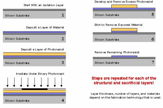
19 Generalized Microfabrication Taken from :
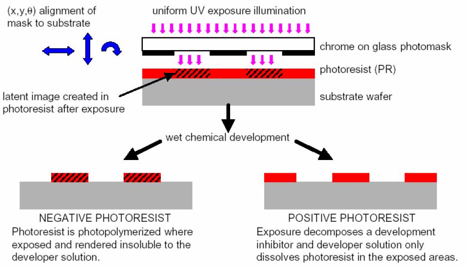
20 Photolithography Clean wafer : to remove particles on the surface as well as any traces of organic, ionic, and metallic impurities Dehydration bake: to drive off the absorbed water on the surface to promote the adhesion of PR Coating : a) Coat wafer with adhesion promoting film (e.g., HMDS) (optional) b) Coat with photoresist Soft bake : to drive off excess solvent and to promote adhesion Exposure Post exposure bake (optional): to suppress standing wave-effect Develop Clean, Dry Hard bake: to harden the PR and improve adhesion to the substrate
21 Photolithography Taken from :
22 Additive Processes Oxidation Thermal Oxidation of Silicon is done in a furnace in wet or dry conditions
23 Additive Processes Doping Purpose of Doping in MEMS - Make P++ etch stop - Change restivity of the film (e.g. make piezoresistor,connecting wire) Dopants : N type (Phosphorous, Arsenic), P type (Boron) Doping Methods 1. Diffusion Dopants are diffused thermally into the substrate in furnace at C. It is governed by Fick s Laws of Diffusion. 2. Ion Implantation Dopant ions bombarded into targeting substrate by high energy. Ion implantation are able to place any ion at any depth in sample.
24 Additive Processes Physical Vapor Deposition (PVD) 1. Evaporation Deposition is achieved by evaporation or sublimation of heated metal onto substrate. This can be done either by resistance heating or by e-beam bombardment. Thermal Evaporator
25 Additive Processes Physical Vapor Deposition (PVD) 2. Sputtering Sputtering is achieved by accelerated inert ion (Ar+) by DC or RF drive in plasma through potential gradient to bombard metallic target. Then the targeting material is sputtered away and deposited onto substrate placed on anode.
26 Additive Processes Physical Vapor Deposition (PVD)
27 Additive Processes Chemical Vapor Deposition (CVD) Materials deposited Polysilicon, silicon nitride (Si3N4), silicon oxide (SiOx), silicon carbide (SiC) etc. How does CVD Work? Gaseous reactants are introduced into chamber at elevated temperatures. Reactant reacts and deposits onto substrate Types of CVD LPCVD (Low Pressure CVD), PECVD (Plasma Enhanced CVD) Salient Features CVD results depend on pressure, gas, and temperature Can be diffusion or reaction limited Varies from film composition, crystallization, deposition rate and electrical and mechanical properties
28 Subtractive Processes Dry Etching 1. Dry Chemical Etching HF Etching HF is a powerful etchant and hence, highly dangerous. XeF 2 Etching 2XeF2+Si 2Xe+SiF4 Isotropic etching (typically 1-3µm/min) Does not attack aluminum, silicon dioxide, and silicon nitride
29 Subtractive Processes Dry Etching Plasma Etching Reaction Mechanism Produce reactive species in gas-phase Reactive species diffuse to the solid Adsorption, and diffuse over the surface Reaction Desorption Diffusion
30 Subtractive Processes Dry Etching 3. Deep Reactive Ion Etching (DRIE) A very high-aspect-ratio silicon etch method (usually > 30:1) BOSCH Process Etch rate is µm/min SF6 to etch silicon Approx. 10nm flourcarbon polymer (similar is plasma deposited using C 4 H 8 Energetic ions (SF + 6 ) remove protective polymer at the bottom trench
31 Subtractive Processes DRIE Etched Pillars
32 Subtractive Processes Wet Etching Isotropic Wet Etching Isotropic etchants etch in all directions at nearly the same rate. Commonly use chemical for Silicon is HNA (HF/HNO 3 /Acetic Acid) This results in a finite amount of undercutting
33 Subtractive Processes Wet Etching Anisotropic Wet Etching Anisotropic etchants etch much faster in one direction than in another. Etchants are generally Alkali Hydroxides (KOH, NaOH, CeOH,..) KOH on silicon Slower etch rate on (111) planes Higher etch rate on (100) and (110) planes (400 times more faster than the (111) plane) Typical concentration of KOH is around 40 wt% Reaction : Silicon (s) + Water + Hydroxide Ions Silicates + Hydrogen
34 Metal Patterning
35 Surface Micromachining
36 Example 1. Pumping membrane 2. Pumping chamber 3. Inlet 4. Outlet 5. Large mesa 6. Upper glass plate 7. Bottom glass plate 8. patterned thin layer (for improved fluidics) An insulin pump fabricated by classic MEMS technology (Surface Micromachining)
37 MEMS Packaging
38 Fabrication of Microfluidic Channels
39 Materials Silicon / Si compounds - Classical MEMS approach - Etching involved Polymers / Plastics - Newer methods - primary die yet needed - easy fabrication of subsequent components
40 Etching Methods Step 1 : Etching of Si - Isotropic / Anisotropic - HNA for isotropic - KOH/EDP/TMAH for anisotropic - RIE can also be used for high aspect ratios
41 Etching Methods Step 2 : Closure of channel a) Bonding another substrate b) LPCVD coating c) Ground Plate Supported Insulating Channels
42 Etching Methods Step 2 : Closure d) Closing Holes in the mask material - channel is defined by a sequence of holes. - channel formed by underetching
43 Etching Methods Step 2 : Closure e) Burying channels beneath surface - Trench made using RIE. - KOH etching to form microchannels - Oxide fills trench
44 Surface Micromachining
45 A Comparative study
46 Using Polymers/Plastics Imprinting and Hot Embossing Injection Molding Laser Photoablation Soft Lithography X ray Lithography (LIGA)
47 Imprinting/Embossing Stamp made in Si or metal Stamp pressed on Plastic to form microfluidic channels Many common plastics successfully imprinted
48 Elastomeric polymer cast in a Si stamp and cured Polymer is peeled off Channel architecture thus transferred to the polymer PDMS technology is becoming popular Soft Lithography
49 Laser Photoablation High aspect ratio channels achievable Laser pulses in the UV region used Sealing by thermal lamination with a PET/PE film at C Depth controllable
50 References otolithographyi.pdf
51 Lecture 9 Biomedical Microtechnology and Nanotechnology Microfabrication and Nanofabrication applied to Biomedical Instrumentation
52 Why Micro/Nano? SCALING OF PARAMETERS The values of various parameters depends on the dimensions of the system and this proves to be helpful in a number of cases. Example : Cantilever bending (Mechanical Parameters) Density of Material = 3.5 x 10 3 kg/m 3 Force F Young s Modulus = N/m 2 Deflection d Material properties such as Young s modulus remain approximately the same in the micro and macro versions. However, they are relatively more different in case of nano dimensions because nano dimensions come closer to molecular level.
53 Why Micro/Nano? SCALING OF PARAMETERS Consider that the dimensions of the cantilever are reduced times, i.e the length, breadth and thickness change from 100 cm, 10cm and 1cm to 100microns, 10 microns and 1 micron respectively. If S represents any dimension in general then, Mass Mass = Density x Volume = Constant x S 3 Therefore mass goes down (10 4 ) 3 or is reduced times as the original beam Strength to Mass Ratio Total strength scales with its cross-sectional area. Hence, total strength scales as S 2. Hence, total strength to mass ratio scales as S -1. As a result, the micro cantilever is 10 4 times stronger than the macro model.
54 Why Micro/Nano? SCALING OF PARAMETERS Deflection Force Young s Modulus 3 Fl 4Fl d = = 3EI Ebt 3 3 breadth Moment of Inertia length thickness Force will vary with cross-sectional area if the stress is to be kept constant Therefore, deflection is proportional to S 1. Therefore, the same stress is generated in the two models if the deflection in the microcantilever is 10-4 times the deflection in the macro model, thus maintaining the bending shape. A much smaller force can be sensed (10-8 times) with the micro cantilever.

55 Why Micro/Nano? SCALING OF PARAMETERS Frequency Frequency scales as the square root of the ratio of the stiffness and mass. Thus, frequency scales as S -1. Hence, micro and nano applications can be high frequency applications. Huang et al have achieved a nanomechanical silicon carbide resonator for ultra high frequency applications. Resonant frequencies have been as high as 632 MHz. Reference :
56 Why Micro/Nano? SCALING OF PARAMETERS Example : Capacitor (Electrical Parameters) If the same electric field E = 10 8 V/m needs to be mainitained between the plates of a micro sized capacitor and a macro sized capacitor, then Voltage Voltage = E x gap Thus, voltage will scale as the gap between the plates. Therefore a much smaller voltage will be required in the micro case to produce the same effect. + V gap gnd
57 Why Micro/Nano? SCALING OF PARAMETERS Electrostatic Force Electrostatic force = Area x (electrostatic field) 2 Thus, electrostatic force scales as S 2 if electrostatic field is maintained same. However, if voltage is to be maintained same, electrostatic force would be independent of scaling. However, its effect in the micro case would be more pronounced because relatively, inertial forces are very low. Electromagnetic force scales as S 4 if magnetic field is to be constant and thus, the world of mems relies on electrostatic motors as opposed to electromagnetic motors. Capacitance Capacitance scales as S 1.


58 Why Micro/Nano? SCALING OF PARAMETERS An electrostatic micromotor An electrostatic comb drive actuator
59 Advantages of Micro/Nano Fluidics for Biomedical Applications Device size for hand-held instrumentation and point-of-care testing is minimal. Provides for efficient use of expensive chemical reagents and low production costs per device allowing disposable microfluidic systems. Precise volumetric control of samples and reagents is possible, which leads to higher sensitivities. High-throughput biological screening is made possible by faster sampling times through parallel processing of samples. In-situ production of unstable compounds for biological assays is also possible. Ratio of surface area to volume is high and thus, the sensing is more effective in case of electrochemical sensors etc.
60 Disadvantages of Micro/Nano Fluidics for Biomedical Applications Bubbles block exits. This could be controlled by either priming at high pressures or by using different priming agents such as ethanol or carbon dioxide. Unwanted particles Fine filtering of solutions becomes important. Surface tension plays funny. Microscale modeling needs to be done and mechanics is not particularly intuitive. However, surface tension forces could be exploited as well! Interfacing with the macroscale equipment is not easy.

61 Micro/Nano applied to BME Taken from :

62 Micro/Nano applied to BME Taken from :


63 Micro/Nano applied to BME Balloon Angioplasty and Stent Procedure ation_art.htm Stent Procedure Balloon Angioplasty es/balloon_stent_gif_big.html

64 Micro/Nano applied to BME Micromachined silicon neural probe arrays Michigan Probe Taken from

65 Micro/Nano applied to BME Drug Delivery Probes

66 Micro/Nano applied to BME


67 Micro/Nano applied to BME An implantable blood pressure sensor developed by CardioMEMS Surgical microgripper actuated by SMA Taken from
68 Micro/Nano Fabrication Techniques

69 Generalized Microfabrication Taken from :
70 Photolithography Clean wafer : to remove particles on the surface as well as any traces of organic, ionic, and metallic impurities Dehydration bake: to drive off the absorbed water on the surface to promote the adhesion of PR Coating : a) Coat wafer with adhesion promoting film (e.g., HMDS) (optional) b) Coat with photoresist Soft bake : to drive off excess solvent and to promote adhesion Exposure Post exposure bake (optional): to suppress standing wave-effect Develop Clean, Dry Hard bake: to harden the PR and improve adhesion to the substrate
71 Photolithography Taken from :


72 Additive Processes Oxidation Thermal Oxidation of Silicon is done in a furnace in wet or dry conditions


73 Additive Processes Doping Purpose of Doping in MEMS - Make P++ etch stop - Change restivity of the film (e.g. make piezoresistor,connecting wire) Dopants : N type (Phosphorous, Arsenic), P type (Boron) Doping Methods 1. Diffusion Dopants are diffused thermally into the substrate in furnace at C. It is governed by Fick s Laws of Diffusion. 2. Ion Implantation Dopant ions bombarded into targeting substrate by high energy. Ion implantation are able to place any ion at any depth in sample.
74 Additive Processes Physical Vapor Deposition (PVD) 1. Evaporation Deposition is achieved by evaporation or sublimation of heated metal onto substrate. This can be done either by resistance heating or by e-beam bombardment. Thermal Evaporator
 by DC or RF drive in plasma through potential gradient to bombard metallic target.")
75 Additive Processes Physical Vapor Deposition (PVD) 2. Sputtering Sputtering is achieved by accelerated inert ion (Ar+) by DC or RF drive in plasma through potential gradient to bombard metallic target. Then the targeting material is sputtered away and deposited onto substrate placed on anode.

76 Additive Processes Physical Vapor Deposition (PVD)
77 Additive Processes Chemical Vapor Deposition (CVD) Materials deposited Polysilicon, silicon nitride (Si3N4), silicon oxide (SiOx), silicon carbide (SiC) etc. How does CVD Work? Gaseous reactants are introduced into chamber at elevated temperatures. Reactant reacts and deposits onto substrate Types of CVD LPCVD (Low Pressure CVD), PECVD (Plasma Enhanced CVD) Salient Features CVD results depend on pressure, gas, and temperature Can be diffusion or reaction limited Varies from film composition, crystallization, deposition rate and electrical and mechanical properties
78 Subtractive Processes Dry Etching 1. Dry Chemical Etching HF Etching HF is a powerful etchant and hence, highly dangerous. XeF 2 Etching 2XeF2+Si 2Xe+SiF4 Isotropic etching (typically 1-3µm/min) Does not attack aluminum, silicon dioxide, and silicon nitride

79 Subtractive Processes Dry Etching Plasma Etching Reaction Mechanism Produce reactive species in gas-phase Reactive species diffuse to the solid Adsorption, and diffuse over the surface Reaction Desorption Diffusion

80 Subtractive Processes Dry Etching 3. Deep Reactive Ion Etching (DRIE) A very high-aspect-ratio silicon etch method (usually > 30:1) BOSCH Process Etch rate is µm/min SF6 to etch silicon Approx. 10nm flourcarbon polymer (similar is plasma deposited using C 4 H 8 Energetic ions (SF + 6 ) remove protective polymer at the bottom trench

81 Subtractive Processes DRIE Etched Pillars
 This results in a finite amount of")
82 Subtractive Processes Wet Etching Isotropic Wet Etching Isotropic etchants etch in all directions at nearly the same rate. Commonly use chemical for Silicon is HNA (HF/HNO 3 /Acetic Acid) This results in a finite amount of undercutting
 KOH on silicon Slower etch rate on (111) planes Higher etch rate on (100) and (110) planes (400 times more faster than the (111) plane) Typical concentration of KOH is around 40 wt% Reaction :")
83 Subtractive Processes Wet Etching Anisotropic Wet Etching Anisotropic etchants etch much faster in one direction than in another. Etchants are generally Alkali Hydroxides (KOH, NaOH, CeOH,..) KOH on silicon Slower etch rate on (111) planes Higher etch rate on (100) and (110) planes (400 times more faster than the (111) plane) Typical concentration of KOH is around 40 wt% Reaction : Silicon (s) + Water + Hydroxide Ions Silicates + Hydrogen
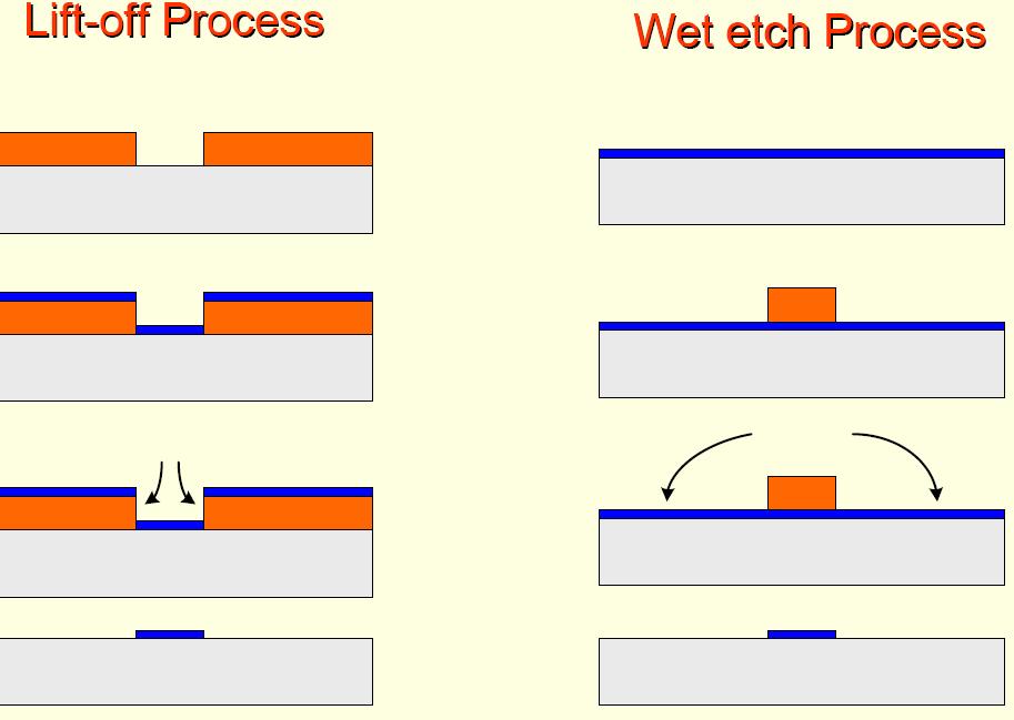
84 Metal Patterning
85 Surface Micromachining
 An insulin pump fabricated by classic MEMS technology (Surface Micromachining)")
86 Example 1. Pumping membrane 2. Pumping chamber 3. Inlet 4. Outlet 5. Large mesa 6. Upper glass plate 7. Bottom glass plate 8. patterned thin layer (for improved fluidics) An insulin pump fabricated by classic MEMS technology (Surface Micromachining)

87 MEMS Packaging
88 Fabrication of Microfluidic Channels
89 Materials Silicon / Si compounds - Classical MEMS approach - Etching involved Polymers / Plastics - Newer methods - primary die yet needed - easy fabrication of subsequent components

90 Etching Methods Step 1 : Etching of Si - Isotropic / Anisotropic - HNA for isotropic - KOH/EDP/TMAH for anisotropic - RIE can also be used for high aspect ratios
 LPCVD coating c) Ground Plate Supported Insulating")
91 Etching Methods Step 2 : Closure of channel a) Bonding another substrate b) LPCVD coating c) Ground Plate Supported Insulating Channels

92 Etching Methods Step 2 : Closure d) Closing Holes in the mask material - channel is defined by a sequence of holes. - channel formed by underetching

93 Etching Methods Step 2 : Closure e) Burying channels beneath surface - Trench made using RIE. - KOH etching to form microchannels - Oxide fills trench
94 Surface Micromachining
95 A Comparative study
96 Using Polymers/Plastics Imprinting and Hot Embossing Injection Molding Laser Photoablation Soft Lithography X ray Lithography (LIGA)
97 Imprinting/Embossing Stamp made in Si or metal Stamp pressed on Plastic to form microfluidic channels Many common plastics successfully imprinted
98 Elastomeric polymer cast in a Si stamp and cured Polymer is peeled off Channel architecture thus transferred to the polymer PDMS technology is becoming popular Soft Lithography

99 Laser Photoablation High aspect ratio channels achievable Laser pulses in the UV region used Sealing by thermal lamination with a PET/PE film at C Depth controllable
100 References otolithographyi.pdf
101 Applications

102 WPI s Nitric Oxide Nanosensor


103 Nitric Oxide Sensor Developed at Dr.Thakor s Lab, BME, JHU Electrochemical detection of NO Left: Schematic of the 16-electrode sensor array. Right: Close-up of a single site. The underlying metal is Au and appears reddish under the photoresist. The dark layer is C (300µm-x-300µm)
104 A E B F C G D H Cartoon of the fabrication sequence for the NO sensor array A) Bare 4 Si wafer B) 5µm of photoresist was spin-coated on to the surface, followed by a pre-bake for 1min at 90 C. C) The samples were then exposed through a mask for 16s using UV light at 365nm and an intensity of 15mW/cm 2. D) Patterned photoresist after development. E) 20nm of Ti, 150nm of Au and 50nm of C were evaporated on. F) The metal on the unexposed areas was removed by incubation in an acetone bath. G)A 2nd layer of photoresist, which serves as the insulation layer, was spun on and patterned. H) The windows in the second layer also defined the microelectrode sites.
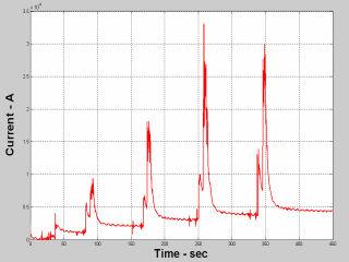
105 NO Sensor Calibration
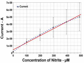
106 NO Sensor Calibration
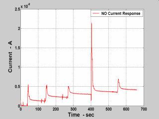
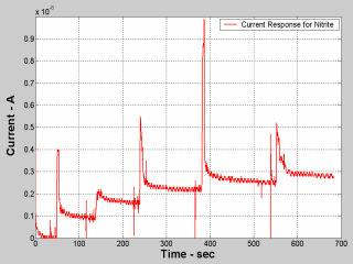
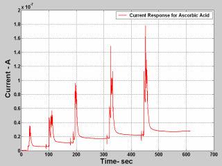
107 Multichannel NO Recordings
108 Michigan Probes for Neural Recordings

109 Neural Recording Microelectrodes Reference : KINDLUNDH.PDF


110 Multi-electrode Neural Recording Reference : Reference :


111 Intraocular Stimulation Electrodes Reference : Lutz Hesse, Thomas Schanze, Marcus Wilms and Marcus Eger, Implantation of retina stimulation electrodes and recording of electrical stimulation responses in the visual cortex of the cat, Graefe s Arch Clin Exp Ophthalmol (2000) 238: