Investigation of the effects of substrate annealing on the properties of polymer blends
|
|
|
- Hector Cain
- 5 years ago
- Views:
Transcription
1 Investigation of the effects of substrate annealing on the properties of polymer blends David E. Motaung 1, 2, Gerald F. Malgas 1,*, Christopher J. Arendse 2,, 1 National Centre for Nano-structured Materials, Council for Scientific Industrial Research, PO. Box 395, Pretoria 0001, South Africa 2 Department of Physics, University of the Western Cape, Private Bag X17, Bellville 7535, South Africa ABSTRACT In this manuscript, we investigated the effect of substrate annealing prior to the deposition of the active layer on the morphological, structural and optoelectrical properties of two variations of organic polymer blends of poly (3- hexylthiophene):c 60 fullerene and poly (3-hexylthiophene):[6,6]-phenyl C 61 butyric acid methyl ester films using atomic force microscopy, field emission scanning microscopy, x-ray diffraction and Hall effect measurements. P3HT films deposited on pre-annealed substrates exhibit an enhancement in the crystallization, and an increase in the electrical conductivity and Hall mobility of p-type P3HT. The microscopic morphology reveals self-assembled fibrillar structures due to the suppressed growth of fullerenes clusters induced by the controlled evaporation rate of the solvent. It is proposed that pre-substrate annealing controls the crystallization of P3HT, the phase separation and diffusion of the acceptor material (C 60 or PCBM). * Corresponding Author: Dr. Gerald Malgas, Tel: (+27) , Fax: (+27) , gmalgas@csir.co.za Corresponding Author: Prof. Christopher Arendse, Tel: (+27) , Fax: (+27) , cjarendse@uwc.ac.za 1
2 Keywords: Poly(-3-hexylthiophene, fullerenes, substrate annealing, morphology. 1. INTRODUCTION Organic photovoltaic cells (OPVs) have attracted great research interests as a potentially low-cost and lightweight source of renewable energy since the first thin film organic PV cell based on a donor/acceptor (D/A) heterojunction was reported by Tang in 1986 [1 3]. Among the various types of polymeric semiconductors, regioregular poly(3-hexylthiophene) (rr-p3ht) is considered as one of the most promising material, due to its good solubility in organic solvents, high hole mobility [4-8] and ease of synthesis [9-11]. Self-organized rr-p3ht exhibits semicrystalline microstructure, consisting of ordered crystallites separated by disordered grain boundary regions, where the crystal domain consists of lamellae of 2D plane with π-π stacked main chains. Efficiencies over 5%, through optimization of processing parameters such as thermal annealing conditions and solvent evaporation time [12-16] 20-24], have been reported. These parameters determine the degree of organization of polymers, nanoscale morphology and have a critical influence on the performance of electronic and optoelectronic devices. It has been reported that thermal annealing at temperatures up to 180 C does not only improve the crystallisation of the rr-p3ht, but also improves the hole mobility of blended films [17-18]. 2
3 Besides the introduction of low-band gap polymers into the photoactive layer, increasing the effective conjugation length and crystallinity of the materials involved in the bulk-heterojunction solar cells is also an efficient way to improve both the match of the optical absorption with the solar spectrum and charge carrier mobility, and eventually the device performance [14, 20-22]. However, no conclusive work has been done using P3HT, C 60 and [6,6]- phenyl-c 61 -butyric acid methyl ester (PCBM) to control and improve the evaporation rate such as by spin-coating an active layer onto an annealed substrate prior to active layer deposition. In this contribution, we therefore report on the effect of substrate annealing, prior to active layer deposition, on the morphology, structural properties and the mobility of two variations of organic polymer blends of poly (3-hexylthiophene):C 60 fullerene and poly (3- hexylthiophene):[6,6]-phenyl C 61 butyric acid methyl ester thin films. 2. EXPERIMENT DETAILS The blended structures were prepared according to the following procedure. Regioregular poly(3-hexylthiophene) (P3HT) with number-average molecular weight M n ~ 64,000 g mol 1 and fullerene (C 60 ) were purchased from Sigma Aldrich and were used as received without further purification. The regioregularity of the P3HT material was specified as > 98.5 %. The active layer containing rr-p3ht (~5mg or a weight percentage of 50 %) and either C 60 or PCBM with concentration (~5 mg) was dissolved in 1 ml of 1,2 dichlorobenzene (DCB) solution to obtain a ratio of 1:1 by weight. DCB has a boiling point of 180 C and a solubility of 28, 30 and >50 mg/ml in fullerene, 3
4 P3HT and PCBM, respectively at room temperature [23, 24]. The solution was stirred overnight on a hotplate at 50 C. No s onication or filtering is used in this process which would adversely affect the polymer side chains and possibly lead to a decrease in the conjugation length of P3HT strands. The thin films were obtained by spin-coating the as-prepared solution onto a hot (annealed) silicon substrate. The spinning rate and time of spin-coating were 2500 rpm and 30 s. In order to control the evaporation rate of the solvent (DCB) from the P3HT films and blends the substrates were annealed at 70 and 110 C on a hot plate for 15 min prior to spin- coating the photoactive layer. The hot substrate may accelerate the evaporation of DCB solvent during spin coating the P3HT films. A Panalytical X pert PRO PW 3040/60 x-ray diffractometer with a Cu K α (λ = nm) monochromated radiation source, operating at 45.0 kv and 40.0 ma was utilized in order to determine the crystallinity of the P3HT blended films. XRD data were collected in the 2θ ranging from 3 to 25 with a step size of The Raman spectroscopy measurements were conducted at room temperature with a 514nm excitation laser with a spectral resolution of 0.4 cm 1. A Tecnai F20 field emission high-resolution transmission electron microscope (FE-HR-TEM), operated at 120 kv was employed to examine the internal structure and crystallinity of P3HT. Specimens for HR-TEM analysis were prepared by transferring a drop of the P3HT solution prepared above to a holey-carbon copper grid and dried at ambient conditions. To quantitatively relate the diffraction intensity in selected area electron diffraction (SAED) patterns to the crystallinity of the specimen investigated, all these SAED 4
5 patterns were performed by using a standard recording mode i.e. fixed magnification, filed-limiting aperture of 100 µm and exposure time of 4.0 s for SAED acquisition. The morphology of the P3HT blended films was investigated by LEO 1525 high resolution field emission scanning electron microscope (HR-FE- SEM) operating at an accelerating voltage of 5 kv. Atomic force microscopy (AFM) images of the top surface of the thin films of P3HT and its blends spin coated on Si (110) substrates in a tapping mode were analyzed using a Veeco AFM system (Digital Instruments) at ambient conditions. The conductivity and the mobility of the P3HT were extracted using a Hall Effect measurement system (ECOPI, HMS-3000). The measurements were carried out at room temperature with a magnetic field of about 0.55 mt. The optical properties of the films were characterized by UV vis absorption measurements. The absorption spectra were obtained using a Perkin-Elmer Lambda 750 UV vis spectrometer. 3. RESULTS AND DISCUSSION 3.1. Structural properties Figure 1 shows the XRD profiles of the as-prepared P3HT films and it blends spin coated on a Si (100) substrate at room temperature (RT) compared with the substrates annealed at different temperatures prior to active layer deposition. The corresponding structural evolution is depicted in Figure 2. The P3HT film spin coated onto the un-annealed Si substrate 5
6 exhibit a weak (100) diffraction peak at 2θ = 5.3. This corresponds to an ordered self-organized lamellar structure with an interlayer spacing, which is formed by parallel stacks of P3HT main chains that are separated by regions that are filled with the alkyl side chains [25-27]. When the Si substrates are annealed at 70 and 110 C a shift in the diffractio n peak to higher 2θ angles (2θ = 5.42 ) is observed, giving a significant decreas e in d-spacing of the (100) plane as depicted in Figure 1 and 2(a). This considerable decrease in the d-spacing with increasing substrate annealing temperature, hints that interdigitation or tilting of the side groups occurred during the formation of ordered aggregates in the solution and induced crystallization during film deposition. The full-width-at-half-maximum (FWHM) reduces, while the crystal size increases linearly with respect to substrate annealing temperature (Fig. 2(b, c)). Similar shifts in the diffraction peaks were also observed by Li et al. [28] by adding a few drops of n-hexane into ODCB solution. The as-prepared samples in the P3HT:C 60 (1:1 weight ratio) and P3HT: PCBM blends (Fig. 1(b, c)), shows no diffraction peaks. This is probably due to the presence of C 60 (or PCBM) molecules, which disturbs the formation of P3HT crystallites at room temperatures. After depositing the blends on a hot substrate the crystallinity of the films drastically increased and a slight shift in the diffraction peaks to lower 2θ angles is observed, (Figure 1(b, c) and 2(b, c)). This increase in crystallinity is probably due to the improved thermal diffusion of C 60 (or PCBM) molecules at elevated temperatures into larger C 60 (or PCBM) aggregates [29-32]. As a result of this motion, regions with low C 60 or PCBM concentration occur, where the P3HT aggregates can convert 6
7 into P3HT crystallites [26]. However, diffraction peaks caused by C 60 (or PCBM) were barely seen in the diffractogram of the blend films both with and without substrate annealing. Thus, substrate annealing only promoted the crystallization of P3HT but had little influence on the crystallization of fullerenes. Therefore, the controlled evaporation rate of the high boiling point solvent (DCB), induced by prior substrate annealing, is an alternative strategy to induce highly ordered and crystalline P3HT in the blended films, which provides an alternative approach to produce organic PV devices with improved efficiencies. To further demonstrate the alterations in the structure, Raman spectroscopy was employed. The intensive Raman bands of P3HT (Figure 3) at 1445 and 1380 cm 1 are due to the C=C stretching vibrations of the thiophene ring and C C skeletal stretching [33-35]. The Raman band of P3HT at 728 cm 1 is assigned to the deformation vibration of the C S C bond. No features attributed to C 60 (or PCBM) could be observed in the Raman spectra. It has been reported by Klimov et al. [33] that the Raman modes of P3HT in the blends are not influenced by the contributions of the C 60 fluorescence. It is can be seen in Figure 3(a, b) that the peak position corresponding to the C=C stretching vibrations exhibit a shift from 1455 to 1450 cm 1 after substrate annealing at 70 ºC and higher temperatures. Such a downward shift in the wave-number is associated with an improvement in the crystallinity of the P3HT polymer and the extension of the effective conjugation length 7
8 along the polymer backbone [36]. However, when the polymer is blended with PCBM in a 1:1 wt. ratio (Figure 3(c)), an improvement in the polymer ordering is only observed after substrate annealing at 110 ºC. Figure 4 shows a bright field TEM image of the P3HT:C 60 (1:1 wt ratio) blend prepared from DCB and the corresponding selected area electron diffraction (SAED) patterns. The SAED patterns in Figure 4a, (spot 1-5) disclose different crystalline ordering in the P3HT:C 60 blends. The SAED of the P3HT:C 60 blend (Figure 4(a)) spot 1, shows a d-spacing of 0.39 and 0.23 nm associated to the reflections from crystallographic (020) planes of typical whisker-like P3HT crystals [37] and diffraction from C 60 nanocrystallites [20, 38]. However, spot 2 shows diffused Debye rings which results from C 60 nanocrystals that are randomly distributed in P3HT matrix. The SAED pattern in spot 3 reveals well-defined rings of high crystallinity as indicated by an arrow, with d-spacing of 0.248, 0.258, 0.86 nm which are ascribed to C 60 nanocrystallites and P3HT. The 0.86 nm d-spacing corresponds to a reflection of (200) of P3HT. As seen in the upper right (spot 4), the SAED pattern of the P3HT:C 60 blend indicates that the central region of sample comprises crystallites of different orientations, corresponding to d-spacing of 0.25, 0.28, 0.19, and 0.39 nm [20, 38]. Since the SAED pattern has been well established for semi-quantitative crystallinity analysis and proven to be a feasible and powerful tool in this field [20, 21, 39], we are able to draw a preliminary conclusion that the crystallization of P3HT blended with C 60 (spot 5, inset) has been substantially 8
9 suppressed, as proven by the low electron diffraction intensity of crystallographic (020) planes of P3HT. The suppression of P3HT by C 60 was also observed in the XRD and Raman results Surface Morphology In order to understand the dependence of the photovoltaic performance on the morphology of the active layer, scanning electron microscopy (SEM) observations were carried out to provide images of the top surfaces of the P3HT and blends. Figure 5 shows SEM micrographs of the as-prepared P3HT and blends compared with that spin coated on Si-substrates annealed at 110 ºC. The as-prepared P3HT film has a smooth surface. When, the substrate is annealed at 110 ºC, rod-like or fibrillar structures are uniformly distributed across the film. The formation of polymer fibrils and dopant islands adhered to the polymer fibrils on a pristine P3HT and doped P3HT films were observed by Singh et al. [40]. The SEM micrograph shows small C 60 aggregates on the surface of the as-prepared substrate of the P3HT:C 60 blended film. Thermal annealing of the film shows that large C 60 clusters in the P3HT:C 60 blend diffused out of the polymer matrix. The blended film of P3HT and PCBM shows only a few small PCBM clusters (circles) embedded in the P3HT matrixes which are separated from each other, while the substrate annealed film at 110 ºC shows fibres with different shapes. It is suggested that these fibres are induced due to a large free volume in the blended films after substrate annealing, allowing the P3HT to readily crystallize. Yang et al. [32] reported that the kinetics of crystal growth of PCBM in the blended films 9
10 is controlled by both the long-range diffusion rate of PCBM molecules and the local incorporation rate of PCBM molecules. In addition, they verified that crystal growth with a relatively low diffusion rate of molecules compared to the incorporation rate, that is, a diffusionlimited system, showed the size increment linearly proportional to the square root of growth time (L t 1/2 ) rather than to growth time (L t). Therefore, we could identify that the highly ordered P3HT crystals (or fibres) suppressed or retarded the diffusion of C 60 or PCBM molecules into the blend under the substrate annealing condition and subsequently limited the enlarged growth of the C 60 or PCBM clusters as depicted in Figure 5 (e) by circles. The micrograph in Figure 5 (d, f) (insets) shows that the surface has clusters/agglomerates of C 60 or PCBM with different sizes distributed across the surface. This is due to the fact that under the thermal-annealing conditions (at 110 ºC), C 60 or PCBM molecules could freely diffuse into the blend films and readily form large PCBM clusters based on three possible causes: (1) a sufficiently large driving force of the external treatment to quickly move C 60 (or PCBM) molecules, (2) a blend film with a too large free volume due to randomly distributed polymer chains and (3) the longer drying time obtained for selectively extracted C 60 molecules to crystallize when a solvent (DCB) with higher solubility of C 60 is used. Initially, high-temperature annealing treatments may force the fast diffusion of PCBM molecules into the blend films and then interrupt the evolution of the highly elongated P3HT crystals. In general, the diffusion is a temperature controlled process that increases with temperature [41]. 10
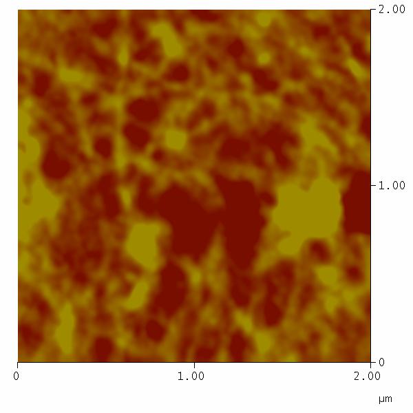
11 In order to observe the morphology evolution much clearer, AFM was used to monitor the height images of P3HT and blended films as shown in Figure 6 and Table 1. Control of the blend morphology at the nanoscale and high charge mobility is essential for polymer photovoltaic devices in terms of their power conversion efficiencies. Hence, it was reported that the donor/acceptor (D/A) blend morphology can be controlled by spin-coating the blend from a specific solvent preventing large-size phase separation or enhancing the polymer chain packing [42, 43]. The as-prepared P3HT film in Fig. 6(a) has a very smooth surface. After substrate annealing at 70 ºC, (Fig. 6(b)) fibres with several micrometers in length are dominantly observed across the film. Moreover, an associated increase in the surface roughness is observed, Table 1. This increase in surface roughness is considered to be a signal of polymer self-organization and phase separation and is in good agreement with results obtained by Motaung et al. [29]. Furthermore, the pre- annealed substrate (110 ºC) with the film deposited thereafter demonstrates more fibres that are locally ordered and appear to be better connected with neighbours. The better connectivity of neighbouring fibres would be expected to make inter-rod transport easier by increasing the electronic overlap between neighbouring fibres, and could explain the increased mobility if transport in films prepared at 70 ºC is limited by the boundaries between the fibres. It is suggested that the P3HT formation of these fibres is due to the early crystallization from presided crystals on a hot substrate before spin-coating due to the controlled evaporation rate. Martens et al. [44] reported that the drying time is an important parameter for the size of the phase separated structures. They showed that by introducing 11
12 a hot air flow over a drying film that the drying time could be decreased and consequently the extent of phase separation reduces. The as-prepared blended film of P3HT and C 60 in Fig. 6(c) exhibited a rather smooth surface, while the substrate annealed (70 ºC) film displayed small C 60 clusters and a slight increase in roughness as shown in Figure 6 (d), implying that the phase separation scale between C 60 and P3HT has been increased. However, the substrate annealed (110 ºC) blended film of P3HT:PCBM (Fig. 6(f)) displayed short fibres, which might have been shortened by an inclusion of PCBM. We conclude that the formation of C 60 crystallites in combination with P3HT fibers contributes to an improved morphology in which not only large interface area for exciton dissociation is preserved but also bi-continuous pathways are constructed for more efficient charge transport through the film. Therefore, better device performance can be anticipated Photo-physical properties Mobility is a key factor for the efficient collection of photogenerated charges in solar cells [45-47]. As illustrated in Figure 7 the mobility and conductivity of P3HT films substantially increases with the substrate annealing temperature. Since the mobility is a function of morphological variables such as the degree of crystallinity, crystallite size, phase domain size [45-47], it can be concluded that the enhancement of mobility is attributed to the improvement in the crystallinity and morphology as observed in the XRD, SEM and AFM analysis. This observation unambiguously confirms also that the increased P3HT crystallinity via the method introduced in this work plays a 12
13 significant role in the improvement of conductivity of the thin film. This increase in conductivity may also be explained from the UV-vis spectra as shown in Fig. 8. The later shows a red shift of 0.02 ev, indicating that the band gap in the P3HT films decreases with the substrate annealing. A slight increase in the absorption coefficient is also observed. This slight increase indicates a significant growth in the conjugation length of the polymer chains in the P3HT film, is induced by the controlled evaporation rate of the solvent during substrate annealing. Such shifts have been observed for conjugated polymers with a strong interchain interaction [15, 48]. It can be concluded that the substrate annealing treatment process enables spatial rearrangement of the polymer chains leading to a tight stacking and a strong interchain interaction. 4. CONCLUSION The ability to control the film-drying rate via substrate annealing, opens a better route to obtain enhanced crystallinity and an optimal morphology. Pre-substrate annealing controls the crystallization of P3HT, the phase separation and diffusion of the acceptor material (C 60 or PCBM) and also increases the electrical conductivity and Hall mobility of p-type P3HT. The SAED patterns revealed different crystallinity behaviours in P3HT:C 60 blends which are mainly attributed to the relative solubility of C 60 with respect to P3HT in DCB. The formation of self-assembled P3HT fibrillar structures that are locally ordered contributes to an improved morphology in which inter-rod 13
14 transport pathways are constructed for more efficient charge transport through the film and therefore, better device performance can be anticipated. 5. AKNOWLWDGEMENTS The authors are grateful for the financial support of the Department of Science and Technology of South Africa, The National Research Foundation (NRF) and the Council for Scientific and Industrial Research (CSIR) of South Africa (Project No. HGERA7S). The authors would like to thank Dr. F. Koch and Mr. Thomas Malwela for assisting with the HR-TEM and AFM analysis. 14
15 6. REFERENCES [1] C. W. Tang, Appl. Phys. Lett. 48 (1986) 183. [2] C. J. Brabec, N. S. Sariciftci, J. C. Hummelen, Adv. Funct. Mater. 11 (2001) 15. [3] S. E. Shaheen, D. S. Ginley, G. E. Jabbour, MRS Bull. 30 (2005) 10. [4] Z. Bao, A. Dodabalapur, A. J. Lovinger, Appl. Phys. Lett. 69 (26) (1996) [5] H. Sirringhaus, N. Tessler, R H. Friend, Science. 280 (5370) (1998) [6] J. F. Chang, B. Sun, D. W. Breiby, M. M. Nielsen, T I. Solling, H. Sirringhaus, Chem. Mater. 16 (2004) [7] D. H. Kim, Y D. Park, Y. Jang, H. Yang, Y H. Kim, K. Cho, et al. Adv. Funct. Mater. 15 (2005) 77. [8] G. Wang, J. Swensen, D. Moses, A. J. Heeger, J. Appl. Phys. 93 (10) (2003) [9] R. S. Loewe, S. M Khersonsky, R. D. McCullough, Adv. Mater. 11 (1999) 250. [10] M. C Iovu, E. E. Sheina, R. R. Gil, R. D. McCullough, Macromolecules 38 (21) (2005) [11] T. A. Chen, X. Wu, R. D. Rieke, J. Am Chem Soc. 117 (1995) 233. [12] A. Hayakawa, O. Yoshikawa, T. Fujieda, K. Uehara, S. Yoshikawa, Appl. Phys. Lett. 90 (2007) [13] S.-I. Na, S.-H. Oh, S.-S. Kim, D.-Y. Kim, Org. Electron. 10 (2009) 496. [14] W. L. Ma, C. Yang, X. Gong, K. Lee, A. J. Heeger, Adv. Funct. Mater. 15 (2005)
16 [15] G. Li, V. Shrotriya, J. Huang, Y. Yao, T. Moriarty, K. Emery, Y. Yang, Nat. Mater. 4 (2005) 864. [16] M. K. Riede, K. O. Sylvester-Hvid, M. Glatthaar, N. Keegan, T. Ziegler, B. Zimmermann, M. Niggenmann, A. W. Liehr, G. Willekr, A. Gombert, Prog. Photovolt: Res. Appl. 16 (2008) 561. [17] H-G. Flesch, R. Resel, C. R. McNeill, Org. Electron. 10 (2009) [18] P. Vanlaeke, A. Swinnen, I. Haeldermans, G. Vanhoyland, T. Aernouts, D. Cheyns, C. Deibel, J. D Haen, P. Heremans, J. Poortmans, J.V. Manca, Solar Energy Materials & Solar Cells 90 (2006) [19] R. B. Koizhaiganova, H. J. Kim, T. Vasudevan, M. S. Lee, Synth. Met. 159 (2009) [20] X. Yang, G. Lu, L. Li, E. Zhou, Small 3 (2007) 611. [21] X. Yang, J. Loos, S. C. Veenstra, W. J. H. Verhees, M. M. Wienk, J. M. Kroon, M. A. J. Michels, R. A. J. Janssen, Nano Lett. 5 (2005) 579. [22] L. H. Nguyen, H. Hoppe, T. Erb, S. Günes, G. Gobsch, N. S. Sariciftci, Adv. Funct. Mater. 17 (2007) 770. [23] R. S. Ruoff, D. S. Tse, R. Malhotra, D. C. Lorents, J. Phys. Chem. 97 (1993) [24] L. Li, H. Tang, H. Wu, G. Lu., X. Yang, Organic Electronics 10 (2009) [25] H. Sirringhaus, P. J. Brown, R. H. Friend, M. M. Nielsen, K. Bechgaard, B. M. W. Langeveld-Voss, A. J. H. Spiering, R. A. J. Janssen, E. W. Meijer, P. Herwig, D. M. de Leeuw, Nature 401 (1999) 685. [26] T. Erb, U. Zhokhavets, G. Gobsch, S. Raleva, B. Stühn, P. Schilinsky, C. Waldauf, C.J. Brabec, Adv. Funct. Mater. 15 (2005)
17 [27] U. Zhokhavets, T. Erb, H. Hoppe, G. Gobsch, N. S. Sariciftci, Thin Solid Films. 496 (2006) 679. [28] L. Li, G. L. and X. Yang, J. Mater. Chem. 18 (2008) [29] D. E. Motaung, G. F. Malgas, C. J. Arendse, S. E. Mavundla, C. J. Oliphant, D. Knoesen, J. Mater. Sci. 44 (2009) [30] H. Hoppe, M. Niggemann, C. Winder, J. Kraut, R. Hiesgen, A. Hinsch, D. Meissner, N. S. Sariciftci, Adv. Funct. Mater. 14 (2004) [31] D. Chirvase, J. Parisi, J. C. Hummelen, V. Dyakonov, Nanotechnology 15 (2004) [32] X. Yang, J. K. J. van Duren, R. A. J. Janssen, M. A. J. Michels, J. Loos, Macromolecules 37 (2004) [33] E. Klimov, W. Li, X. Yang, G. G. Hoffmann, J. Loos, Macromolecules 39 (2006) [34] D. E. Motaung, G. F. Malgas, C. J. Arendse, S. E. Mavundla, C. J. Oliphant, D. Knoesen, Solar Energy Materials & Solar Cells 93 (2009) [35] P. J. Brown, D. S.T homas, A. Kohler, J. S. Wilson, J.-S. Kim, C. M. Ramsdale, H. Sirringhaus, R. H. Friend, Phys. Rev. B 67 (2003) [36] C. Heller, G. Leising, G. Godon, S. Lefrant, W. Fischer, F. Stelzer, Phys. Rev., B 51 (1995) [37] K. Tashiro, M. Kobayashi, T. Kawai, K. Yoshino, Polymer 38 (1997) [38] C. Y. Yang, A. J. Heeger, Synth. Met. 83 (1996) 85. [39] J. X. Geng, T. Y. Zeng, J. Am. Chem. Soc. 128 (2006)
18 [40] R. K. Singh, J. Kumar, R. Singh, R. Kant, S. Chand, V. Kumar, Materials Chemistry and Physics 104 (2007) 390. [41] W. D. Callister, Jr., Materials Science and Engineering: An Introduction, 5 th ed., John Wiley, New York [42] S. E. Shaheen, C. J. Brabec, N. S. Sariciftci, F. Padinger, T. Fromerz, J. C. Hummelen, Appl. Phys. Lett. 78 (2001) 841. [43] J. K. J. van Duren, X. Yang, J. Loos, C. W. T. Bulle-Lieuwma, A. B. Sieval, J. C. Hummelen, R. A. J. Janssen, Adv. Funct. Mater. 14 (2004) 425. [44] T. Martens, Z. Beelen, J. D Haen, T. Munters, L. Goris, J. Manca, M. Proc. SPIE-Int. Soc. Opt. Eng., 40 (2003) [45] G. Tu, A. Bilge, S. Adamczyk, M. Forster, R. Heiderhoff, L. J. Balk, D. Muhlbacher, M. Morana, M. Koppe, M. C. Scharber, S. A. Choulis, C. J. Brabec, U. Scherf, Macromol. Rapid Commun. 28 (2007) [46] H. Xin, F. S. Kim, S. A. Jenekhe, J. Am. Chem. Soc. 130 (2008) [47] M. Dante, J. Peet, T. Q. Nguyen, J. Phys. Chem. C 112 (2008) [48] D. E. Motaung, G. F. Malgas, C. J. Arendse, S. E. Mavundla, D. Knoesen, Materials Chemistry and Physics 116 (2009)
19 LIST OF FIGURES CAPTIONS AND TABLES Figure 1: XRD profiles of (a) P3HT and (b) P3HT:C 60 (c) P3HT:PCBM films spin-coated onto an un-annealed Si substrates and substrates annealed at 70 and 110 C for 15 min. Figure 2: Structural evolution of P3HT crystals in blends films during substrate annealing (a) d-spacing, (b) FWHM of the P3HT (100) peak and (c) the average P3HT (100) crystal size. Figure 3: Raman spectra of the as-prepared, substrate annealed films of (a) P3HT, (b) P3HT:C 60 (1:1 wt. ratio) and (c) P3HT:PCBM (1:1 wt. ratio) blends. Figure 4: Bright field-tem images of (a) P3HT:C 60 dissolved in DCB solution and the corresponding SAED patterns obtained at different spots as denoted by circles in Fig. 4(a). Figure 5: FE-SEM micrographs of P3HT (a) un-annealed substrate, (b) substrate annealed at 110 ºC, micrographs of P3HT:C 60 (c) unannealed substrate, (d) substrate annealed at 110 ºC, micrographs of P3HT:PCBM (e) un-annealed substrate and (f) substrate annealed at 110ºC. The inset in (d) and (f) correspond to films thermally annealed at 110 ºC. Figure 6: AFM height images of P3HT (a) un-annealed substrate, (b) substrate annealed at 70 ºC, (c) 110 ºC, images of P3HT:C 60 (d) un-annealed substrate, (e) substrate annealed at 70 ºC, (f) 110 ºC, images of P3HT:PCBM (g) un-annealed substrate and (h) substrate annealed at 70ºC and (i) 110 ºC. 19
20 Figure 7: Hall measurements on (a) the Mobility and (b) conductivity of P3HT films as a function of substrate annealing temperature annealing. Figure 8: UV-vis absorption spectra of the as-prepared and substrate annealed (a) P3HT films and (b) P3HT:PCBM (1:1 wt. ratio) blends. Table 1: Root-mean-square roughness for different substrate annealing temperatures of P3HT and blended films. 20
21 (a) (b) (c) 21
22 (a) (b) (c) 22
23 (a) (b) (c) 23
")
 1.")
")


24 (5) 1.1/nm (a) 1 µm (1) (2) 1.1/nm 1.1/nm (3) (4) 1.1/nm 1.1/nm 24

 2 µm")
 2 µm")


25 (a) (b) 10 µm 1 µm (c) (d) 2 µm 10 µm 1 µm (f) (e) 2 µm 2 µm 2 µm 25
 (d)")
 (h)")


26 (a) (b) (c) (d) (e) (f) (g) (h) (i) 26
27 (a) (b) 27
28 (a) (b) 28
29 Samples Root-mean-square (rms) roughness (nm) Substrate annealed at 70 ºC Un-annealed Sisubstrate Substrate annealed at 110 ºC P3HT P3HT:C P3HT:PCBM