Single vs Polycrystals
|
|
|
- Ambrose Godwin Barrett
- 5 years ago
- Views:
Transcription
1 WEEK FIVE This week, we will Learn theoretical strength of single crystals Learn metallic crystal structures Learn critical resolved shear stress Slip by dislocation movement
2 Single vs Polycrystals Polycrystals 200 mm -Properties may/may not vary with direction. If grains are randomly oriented: isotropic. (E poly iron = 210 GPa) If grains are textured, anisotropic. Macroscopically homogeneous but Microscopically heterogeneous Grain boundaries Second phase particles It is therefore easier to study plastic deformation in a single crystal to eliminate the effects of grain boundaries and second phase particles.

3 Slip in a Perfect Lattice Slip is assumed to occur by translation of one plane of atoms over another A perfect bcc lattice, 2000 atoms Therefore consider two planes of atoms subjected to a homogeneous shear stress Shear stress is assumed to act in a slip plane along the slip direction The distance between the atoms in the slip direction is b The spacing between adjacent lattice is a The shear stress cause a displacement x in the slip direction between the pair of adjacent lattice planes
4 Slip in a Perfect Lattice The energy is minimum at the equilibrium point P. If one plane is displaced, stored energy first increases, reaches a maximum at half lattice spacing and then returns to minimum at one lattice spacing. and t=f/a The shear stress is zero when two planes are in coincidence, initial stage Shear Force t m (c) When the two planes have move one identity distance atoms of the top plane are midway between those of the bottom plane Shearing stress is a periodic function of the displacement from zero at P, Q and R to a max value at b/4 and 3b/4 Therefore shear stress may be expressed in the sinusoidal variation in energy through out the lattice
5 Strength of perfect crystall and => Because of the approximations made in this analysis the magnitude of the theoretical shear stress t m is of an approximate nature. More realistic estimates in the range of G/15.
6 Theoretical and experimental yield strengts in various materials
7 x z Crystallographic Directions y Algorithm 1. Vector repositioned (if necessary) to pass through origin. 2. Read off projections in terms of unit cell dimensions a, b, and c 3. Adjust to smallest integer values 4. Enclose in square brackets, no commas [uvw] ex: 1, 0, ½ => 2, 0, 1 => [ 201 ] -1, 1, 1 => [ 111 ] where over bar represents a negative index families of directions <uvw>
8 HCP Crystallographic Directions Hexagonal Crystals 4 parameter Miller-Bravais lattice coordinates are related to the direction indices (i.e., u'v'w') as follows. z [ u 'v 'w ' ] [ uvtw ] u = 1 3 ( 2 u ' - v ') a 3 a 2 - v t = = 1 3 ( 2 v ' - u - ( u + v ) ') a 1 w = w ' Fig. 3.8(a), Callister 7e.
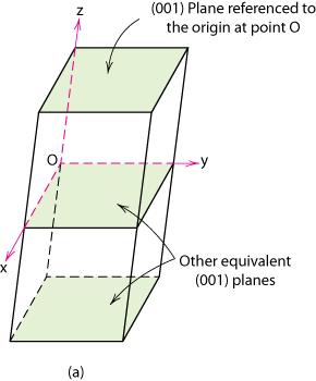
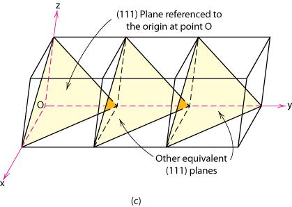
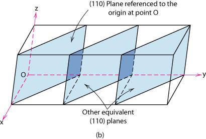
9 Crystallographic Planes Miller Indices: Reciprocals of the (three) axial intercepts for a plane, cleared of fractions & common multiples. All parallel planes have same Miller indices. Notation: enclose in parentheses, no commas i.e., (hkl) z example a b c 1. Intercepts 1/2 2. Reciprocals 1/½ 1/ 1/ 4. Miller Indices (100) Reduction Notice: Miller indices also gives the vector normal to the surface. Family of Planes {hkl} x a c b y Ex: {100} = (100), (010), (001), (100), (010), (001)
10 Crystallographic Planes Adapted from Fig. 3.9, Callister 7e.
11 Crystallographic Planes (HCP) z In hexagonal unit cells the same idea is used example a 1 a 2 a 3 c 1. Intercepts Reciprocals 1 1/ Reduction a 2 4. Miller-Bravais Indices (1011) a 3 a 1 Adapted from Fig. 3.8(a), Callister 7e. Plastic deformation is generally confined to the low-index planes, which has higher density of atom per unit area. The planes of greatest atomic density also are the most widely spaced planes for the crystal structure.
12 Simple relationships between a direction and a plane For cubic system there are simple relationships between a direction [uvw] and a plane (hkl). 1) [uvw] is normal to (hkl) when u = h; v = k, w = l. [111] is normal to (111). 2) [uvw] is parallel to (hkl), when hu + kv + lw = 0. 3) Two planes (h 1 k 1 l 1 ) and (h 2 k 2 l 2 ) are normal if h 1 h 2 + k 1 k 2 + l 1 l 2 = 0. 4) Two directions u 1 v 1 w 1 and u 2 v 2 w 2 are normal if u 1 u 2 + v 1 v 2 + w 1 w 2 = 0. 5) Angles between planes (h 1 k 1 l 1 ) and (h 2 k 2 l 2 ) are given by (a. b = a b cos q)
13 Metallic Crystal Structures Tend to be densely packed. Reasons for dense packing: - Typically, only one element is present, so all atomic radii are the same. - Metallic bonding is not directional. - Nearest neighbor distances tend to be small in order to lower bond energy. - Electron cloud shields cores from each other Have the simplest crystal structures. We will examine three such structures...
, Tantalum, Molybdenum length = 4R = 3 a APF for a body-centered cubic structure = 0.")
14 Body Centered Cubic Structure (BCC) Atoms touch each other along cube diagonals. ex: Cr, W, Fe ( ), Tantalum, Molybdenum length = 4R = 3 a APF for a body-centered cubic structure = 0.68 Close-packed plane: {110} closely followed by {112} and {113} Close-packed direction: [111]

15 Face Centered Cubic Structure (FCC) Atoms touch each other along face diagonals. ex: Al, Cu, Au, Pb, Ni, Pt, Ag length = 4R = 2 a APF for a face-centered cubic structure = 0.74 Close-packed plane: {111} Close-packed direction: [110]
16 Hexagonal Close-Packed Structure (HCP) ABAB... Stacking Sequence ex: Cd, Mg, Ti, Zn 3D Projection 2D Projection A sites Top layer c B sites Middle layer a A sites Bottom layer APF = 0.74 c/a = Close-packed plane: {0001} Basal plane Close-packed direction:

17 Real crystals deviate from the perfect periodicity that was assumed in a number of ways. While the concept of the perfect lattice is adequate for explaining structure-insensitive properties of metals, for a better understanding of the structure-sensitive properties it has been necessary to consider lattice defects. Lattice Defects Point defects Line defects Surface defects Volume defects
18 Point defects (a) Vacancy (b) interstitial (c) Impurity atom a) Vacancy : an atom is missing from a normal lattice position. b) Interstitial atom : an atom that is trapped inside the crystal at a point intermediate between normal lattice positions. c) Impurity atom : Impurity atom which is present in the lattice, resulting in local disturbance of the lattice. (maybe interstitial or substitutional)
19 Vacancies The equilibrium number of vacancies formed as a result of thermal vibrations may be calculated from thermodynamics: N s : number of regular lattice sites, k B :Boltzmann constant (1.38x10⁻²³ J/atom K) Q v :energy needed to form a vacant lattice site in a perfect crystal, T : temperature in Kelvin. Nv Ns exponential dependence T


20 Solid Solutions Second phase particle --different composition --often different structure.
21 Dislocations Dislocation is a linear or one-dimensional defect. Dislocations are responsible for the slip phenomenon, by which most metals deform plastically. before deformation after tensile elongation slip steps Dislocations are also intimately connected with nearly all other mechanical properties such as strain hardening, yield point, creep, fatigue and brittle fracture. There are two basic types of dislocations; 1) Edge dislocation 2) Screw dislocation

22 Slip by dislocation motion Slip is a plastic deformation process produced by dislocation motion. Dislocation motion is analogous to the caterpillar movement model. The caterpillar forms a hump with its position and movement corresponding to those of extra-half plane in the dislocation model.
, while those below are pulled apart (tensile), causing localised lattice distortion.")
23 Edge dislocation Edge dislocation is a linear defect that centres around the line that is defined along the end of the extra portion of a plane of atoms (half plane), Atoms above dislocation line are squeezed together (compressive), while those below are pulled apart (tensile), causing localised lattice distortion. b Compression Tension The amount of displacement = the Burgers vector b of the dislocation
 is linear along the dislocation line.")
24 Screw dislocations Screw dislocation may be thought of as being formed by applying a shear stress to produce a distortion. The atomic distortion (a shift of one atomic distance to the right) is linear along the dislocation line. Every time a circuit is made around the dislocation line, the end point is displaced one plane parallel to the slip plane in the lattice resulting in a spiral or staircase or screw.
25 Deformation by dislocations An edge dislocation: the dislocation line moves in the direction of the applied shear stress τ. Edge Burgers vector is perpendicular to the dislocation line. A screw dislocation: the dislocation line motion is perpendicular to the stress direction. Screw Burgers vector is parallel to the dislocation line. Both shear stress and final deformation are identical for both situations.
26 Stress and Dislocation Motion Crystals slip due to a resolved shear stress, t R. Applied tension can produce such a stress. Applied tensile stress: s = F/A A F F Resolved shear stress: t R =Fs/As slip plane normal, n s t R F S t R A S Relation between s and t R t R = F S /A S Fcos l F l F S n S A/cos f f A S A t R= s cosf cosl
27 Critical resolved shear stress for slip The extent of slip in a single crystal depending on: 1) The magnitude of the shear stress 2) The geometry of the crystal structure 3) The number of active slip plane in the shear stress direction. Slip occurs when the shearing stress on the slip plane in the slip direction reaches a critical resolved shear stress. Schmid calculated the critical resolved shear stress from a single crystal tested in tension. The area of the slip plane A = A/cosφ. The force acting in the slip plane A is Pcosλ The critical resolved shear stress is given by t R= s cosf cosl is called the Schmid Factor
28 Critical Resolved Shear Stress Condition for dislocation motion: t R t CRSS Crystal orientation can make it easy or hard to move dislocation t R = scos lcos f s s typically 0.1 MPa to 10 MPa s l =90 t R = 0 t R = s/2 l =45 f =45 f =90 t R = 0 t maximum at l = f = 45º
 (cos35 )(cos60 ) = (6500 psi) (0.")
29 Ex: Deformation of single crystal f=60 l=35 a) Will the single crystal yield? b) If not, what stress is needed? t crss = 3000 psi t = s cos l cos f s = 6500 psi Adapted from Fig. 7.7, Callister 7e. s = 6500 psi So the applied stress of 6500 psi will not cause the crystal to yield. t = (6500 psi) (cos35 )(cos60 ) = (6500 psi) (0.41) t = 2662 psi t crss = 3000 psi
30 Ex: Deformation of single crystal What stress is necessary (i.e., what is the yield stress, s y )? t crss = 3000 psi = s y cos l cos f = s y (0.41) s y = t cos lcos f 3000 psi 0.41 crss = = 7325 psi So for deformation to occur the applied stress must be greater than or equal to the yield stress s s y = 7325 psi
31
. Produce imperfection in crystal structures Effects mechanical properties of materials.")
32 Dislocations Dislocations introduce imperfection into the structure and therefore these could explain how real materials exhibit lower yield stress value than those observed in theory. Lower the yield stress from theoretical values. Produce plastic deformation (strain hardening). Produce imperfection in crystal structures Effects mechanical properties of materials.
33 Defects and CRSS Variation of critical resolved shear stress with composition in silver-gold alloy single crystal. Defects Vacancies Impurity atoms Alloying elements Strength of metal crystals as a function of dislocation density. Critical resolved shear stress Logarithmic scale