Crosslink Product Family Qualification Summary
|
|
|
- Gabriel Bradley
- 5 years ago
- Views:
Transcription

1 Crosslink Product Family Qualification Summary Lattice Document # June Lattice Semiconductor Corp. All Lattice trademarks, registered trademarks, patents, and disclaimers are listed at All other brand or product names are trademarks or registered trademarks of their respective holders. The specifications and information herein are subject to change without notice.
2 Dear Customer, Enclosed is Lattice Semiconductor s Crosslink Product Family Qualification Summary Report. This report was created to assist you in the decision making process of selecting and using our products. The information contained in this report represents the entire qualification effort for this device family. The information is drawn from an extensive qualification program of the wafer technology and packaging assembly processes used to manufacture our products. The program adheres to JEDEC and Automotive Industry standards for qualification of the technology and device packaging. This program ensures you only receive product that meets the most demanding requirements for Quality and Reliability. Your feedback is valuable to Lattice. If you have suggestions to improve this report, or the data included, we encourage you to contact your Lattice representative. Sincerely, James M. Orr Vice President, Corporate Quality Lattice Semiconductor Corporation 2
3 TABLE OF CONTENTS 1.0 INTRODUCTION... 4 Table CrossLink Product Family Attributes LATTICE PRODUCT QUALIFICATION PROGRAM... 6 Figure Lattice Standard Product Qualification Process Flow...6 Table Qualification Tests for Components in Non-Hermetic Packages QUALIFICATION DATA CROSSLINK PRODUCT FAMILY CrossLink Product Family Life (HTOL) Data...10 Table CrossLink Product Family Life Results CrossLink Product Family ESD and Latch UP Data...12 Table CrossLink ESD-HBM Data Table CrossLink ESD-CDM Data Table CrossLink I/O Latch Up HOT (105 C) Data Table CrossLink Vcc Latch Up HOT (105 C) Data PACKAGE QUALIFICATION DATA FOR CROSSLINK PRODUCT FAMILY Table Summary of Package Reliability Test Conditions and Results Surface Mount Preconditioning Testing...15 Table Surface Mount Precondition Data Temperature Cycling (TC)...16 Table Temperature Cycling Data Biased HAST...17 Table Biased HAST Data Unbiased HAST...18 Table Unbiased HAST Data High Temperature Storage Life...19 Table High Temperature Storage Life Data ADDITIONAL PACKAGE FAMILY DATA Table CrossLink Product Family Bills of Material by Package Type and Assembly Site REVISION HISTORY Table CrossLink Product Family Qualification Summary Revisions
4 1.0 INTRODUCTION CrossLink from Lattice Semiconductor is a programmable video bridging device that supports a variety of protocols and interfaces for mobile image sensors and displays. The device is based on Lattice mobile FPGA 40nm technology. It combines the extreme flexibility of an FPGA with the low power, low cost and small footprint of an ASIC. CrossLink supports video interfaces including MIPI DPI, MIPI DBI, CMOS camera and display interfaces, OpenLDI, FPD-Link, FLATLINK, MIPI D-PHY, MIPI CSI-2, MIPI DSI, SLVS200, SubLVDS, HiSPi and more. Lattice Semiconductor provides many pre-engineered IP (Intellectual Property) modules for CrossLink. By using these configurable soft core IPs as standardized blocks, designers are free to concentrate on the unique aspects of their design, increasing their productivity. The Lattice Diamond design software allows large complex designs to be efficiently implemented using CrossLink. Synthesis library support for CrossLink devices is available for popular logic synthesis tools. The Diamond tools use the synthesis tool output along with the constraints from its floor planning tools to place and route the design in the CrossLink device. The tools extract the timing from the routing and back-annotate it into the design for timing verification. Interfaces on CrossLink provide a variety of bridging solutions for smart phone, tablets, wearables, VR, AR, Drone, Smart Home, HMI as well as adjacent ISM markets. The device is capable of supporting high-resolution, highbandwidth content for mobile cameras and displays at 4k UHD and beyond. 4
5 Table CrossLink Product Family Attributes Device CrossLink LUTs 5936 sysmem Blocks (9kb) 20 Embedded Memory (kb) 180 Distributed RAM Bits (kb) 47 General Purpose PLL 1 NVCM Yes Embedded I2C 2 Oscillator (10 KHz) 1 Oscillator (48 MHz) 1 Hardened MIPI D-PHY 2 1,2 Packages I/O 36 WLCSP (2.5x25. mm2) 17 64ucfBGA (3.5x3.5 mm2) ctfbga (6.5x6.5 mm2) 36 81csfBGA (4.5x4.5 mm2) 37 Notes: 1. Additional D-PHY Rx interfaces are available using programmable I/O. 2. Only one Hardened D-PHY is available in 36 WLCSP package. 5
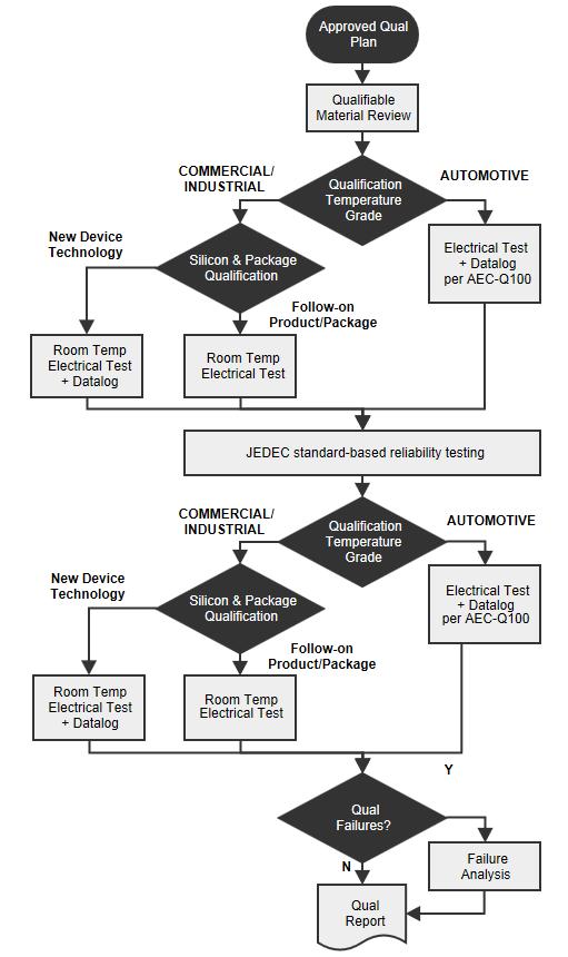
6 2.0 LATTICE PRODUCT QUALIFICATION PROGRAM Lattice Semiconductor Corp. maintains a comprehensive reliability qualification program to assure that each product achieves its reliability goals. After initial qualification, the continued high reliability of Lattice products is assured through ongoing monitor programs as described in Lattice Semiconductor s Reliability Monitor Program Procedure (Doc. # ). All product qualification plans are generated in conformance with Lattice Semiconductor s Qualification Procedure (Doc. # ) with failure analysis performed in conformance with Lattice Semiconductor s Failure Analysis Procedure (Doc. # ). Both documents are referenced in Lattice Semiconductor s Quality Assurance Manual, which can be obtained upon request from a Lattice Semiconductor sales office. Figure shows the Product Qualification Process Flow. If failures occur during qualification, an 8D process is used to find root cause and eliminate the failure mode from the design, materials, or process. The effectiveness of any fix or change is validated through additional testing as required. Final testing results are reported in the qualification reports. Product families are qualified based upon the requirements outlined in Table In general, Lattice Semiconductor follows the current JEDEC Solid State Technology Association JESD47 Stress-Based Qualification testing methods. Package family qualification will include products with a wide range of circuit densities, package types, and package lead counts. Major changes to products, processes, or vendors require additional qualification before implementation in production. Lattice Semiconductor maintains a regular reliability monitor program. The current Lattice Reliability Monitor Report can be found at Product Reliability Monitor Report. 6

7 Figure Lattice Standard Product Qualification Process Flow This diagram represents the standard qualification flow used by Lattice to qualify new Product Families. The target end market for the Product Family determines which flow options are used. The CrossLink Product Family was qualified using the Commercial / Industrial Qualification Option. 7
8 8
9 Table Qualification Tests for Components in Non-Hermetic Packages TEST STANDARD TEST CONDITIONS High Temperature Operating Life (HTOL) JESD22-A C Tj and max operating supplies Human Body Model ESD (HBM) JS C (Technology/Device dependent Performance Targets) Charged Device Model ESD (CDM) JS C (Technology/Device dependent Performance Targets) Latch-Up (LU) JESD78 Class II, +/-100mA trigger current and AMR operating supplies Accelerated Soft Error Testing (ASER) JESD89 25 C, Nominal operating supplies Surface Mount Preconditioning (SMPC) IPC/JEDEC J-STD-020 Per appropriate MSL level per J-STD-020 High Temp Storage Life (HTSL) JESD22-A103 Condition B Temperature Cycling (TC) Temperature Humidity Bias, THB (85/85) or Biased HAST (HAST) Unbiased Temperature/Humidity (UHAST) JESD22-A104 JESD22-A101 JESD22-A110 JESD22-A118 Condition B, soak mode 2 (typical) 85 C, 85 % RH, max operating supplies or 110 C, 85 % RH, max operating supplies or 130 C, 85 % RH, max operating supplies 110 C, 85 % RH or 130 C, 85 % RH 9
10 3.0 QUALIFICATION DATA CROSSLINK PRODUCT FAMILY The Crosslink devices are fabricated at UMC based on Lattice mobile FPGA 40nm technology then assembled and tested at Advanced Semiconductor Engineering, Kaohsiung (ASET). The LIF-MD6000-MG81 is the lead product qualification vehicle for this family. Product Family: LIF-MD6000 Packages offered: csfbga Process Technology Node: 40 nm 10
11 3.1 CrossLink Product Family Life (HTOL) Data High Temperature Operating Life (HTOL) Test The High Temperature Operating Life test is used to thermally accelerate those wear out and failure mechanisms that would occur as a result of operating the device continuously in a system application. Consistent with EIA/JESD22-A108E Temperature, Bias, and Operating Life, a pattern specifically designed to exercise the maximum amount of circuitry is programmed into the device and this pattern is continuously exercised at specified voltages as described in test conditions for each device type. CrossLink Life Test (HTOL) Conditions: Stress Duration: 1000 hours Stress Conditions: CrossLink: HTOL Pattern, Vcc=1.32V, Vccio=3.63V, TJUNCTION = >125 C Method: EIA/JESD22-A108E Table CrossLink Product Family Life Results Product Name Foundry Lot # Qty 48 Hrs Result 168 Hrs Result 500 Hrs Result 1000 Hrs Result Cumulative Hours LIF-MD6000 UMC N/A ,000 LIF-MD6000 UMC N/A ,000 LIF-MD6000 UMC N/A ,000 LIF-MD6000 UMC 4 85 N/A ,000 LIF-MD6000 UMC 5 85 N/A ,000 LIF-MD6000 UMC 6 85 N/A ,000 *Vcc=1.32V (Absolute Maximum Rating for Vcc). Crosslink HTOL Cumulative Result / Sample Size = 1 / 555 Crosslink Cumulative Life Testing Device Hours = 554,000 Crosslink Long Term Failure Rate < 50 FITs Crosslink FIT Assumptions: CL=60%, Ea=0.7eV, Tjref=55C 1 *FAR# 1631: 1 unit with marginal pin leakage failure 11
12 3.2 CrossLink Product Family ESD and Latch UP Data Electrostatic Discharge-Human Body Model CrossLink product family was tested per the JS Electrostatic Discharge (ESD) Sensitivity Testing Human Body Model (HBM) procedure. All units were Class tested at room ambient prior to reliability stress and after reliability stress. No failures were observed within the passing classification. Table CrossLink ESD-HBM Data Product 64 ucfbga (3.5.5x.3.5mm, 0.5mm 80 ctfbga (6.5x6.5mm, 0.5mm LIF-MD6000 QBS QBS 81 csfbga (4.5x4.5mm, 0.5mm HBM>2kV Class 2 HBM classification for Commercial/Industrial products per JS All HBM levels indicated are dual-polarity (±). HBM worst-case performance is the package with the smallest RLC parasitics. All other packages for a given product are qualified-by-similarity (QBS). Electrostatic Discharge-Charged Device Model: CrossLink product family was tested per the JS , Field-Induced Charged-Device Model Test Method for Electrostatic-Discharge-Withstand Thresholds of Microelectronic Components procedure. All units were Class tested at room ambient prior to reliability stress and after reliability stress. No failures were observed within the passing classification. Table CrossLink ESD-CDM Data Product 64 ucfbga (3.5.5x.3.5mm, 0.5mm 80 ctfbga (6.5x6.5mm, 0.5mm LIF-MD6000 QBS QBS 81 csfbga (4.5x4.5mm, 0.5mm CDM>1kV Class C3 CDM classification for Commercial/Industrial products, per EIA/JESD22-C101. All CDM levels indicated are dual-polarity (±). CDM worst-case performance is the package with the largest bulk capacitance. All other packages for a given product are qualified-by-similarity (QBS). 12
13 Latch-Up: CrossLink product family was tested per the JESD78D IC Latch-up Test procedure. All units were Class tested at room ambient prior to reliability stress and after reliability stress. No failures were observed within the passing classification. Table CrossLink I/O Latch Up HOT (105 C) Data Product 64 ucfbga (3.5.5x.3.5mm, 0.5mm 80 ctfbga (6.5x6.5mm, 0.5mm LIF-MD6000 QBS QBS 81 csfbga (4.5x4.5mm, 0.5mm > +/-100mA Class II I-Test LU classification for Commercial/Industrial products, per JESD78D. All IO-LU levels indicated are dual-polarity (±). IO-LU worst-case performance is the package with access to the most IOs. All other packages for a given product are qualified-by-similarity (QBS). Table CrossLink Vcc Latch Up HOT (105 C) Data Product 64 ucfbga (3.5.5x.3.5mm, 0.5mm 80 ctfbga (6.5x6.5mm, 0.5mm LIF-MD6000 QBS QBS 81 csfbga (4.5x4.5mm, 0.5mm > 1.5x Vcc Class II Vsupply Over-voltage Test LU classification for Commercial/Industrial products, per JESD78D. Vcc-LU worst-case performance is the package with access to the most individual power rails. All other packages for a given product are qualified-by-similarity (QBS). 13
14 4.0 PACKAGE QUALIFICATION DATA FOR CROSSLINK PRODUCT FAMILY The CrossLink devices are assembled and tested at Advanced Semiconductor Engineering, Kaohsiung Taiwan (ASET). Package qualification tests include Surface Mount Pre-Conditioning (SMPC), Temperature Cycling (T/C), Biased HAST (BHAST), Unbiased HAST (UHAST) and High Temperature Storage (HTSL). Electrical test is performed pre- and post-stress. Mechanical evaluation tests include Scanning Acoustic Tomography (SAT) and Visual Package Inspection. Table Summary of Package Reliability Test Conditions and Results Assembly Lot Cumulative Device # of Test Stress Conditions Test Vehicle Package Type Site Quantity Units/Hours/Cycles Fails 81-csfBGA 6 1,628 units 0 64-ucfBGA Q4 17 ASET SMPC 3x 260 C reflow LIF-MD ctfBGA Q WLCSP Q4 17 ASET TC -55 C to 125 C LIF-MD csfBGA 6 441,000 cycles 0 64-ucfBGA Q ctfBGA Q WLCSP Q4 17 ASET ASET BHAST UHAST 81-csfBGA 6 140,184 hours 0 85%RH, 110 C, 264 hours 64-ucfBGA Q4 17 LIF-MD ctfBGA Q %RH, 130 C, 96 hours 36-WLCSP Q csfBGA 6 140,184 hours 0 85%RH, 110 C, 264 hours 64-ucfBGA Q4 17 LIF-MD ctfBGA Q %RH, 130 C, 96 hours 36-WLCSP Q4 17 ASET HTSL 150 C, 1000 hours LIF-MD csfBGA 6 435,000 hours 0 64-ucfBGA Q ctfBGA Q WLCSP Q
15 4.1 Surface Mount Preconditioning Testing The Surface Mount Preconditioning (SMPC) Test is used to model the surface mount assembly conditions during component solder processing. All devices stressed through High Temperature Storage, Temperature Cycling, Un-biased HAST and Biased HAST were preconditioned. This preconditioning is consistent with J-STD-020D and JEDEC JESD22-A113F Preconditioning Procedures of Plastic Surface Mount Devices Prior to Reliability Testing. Surface Mount Preconditioning (MSL3): (5cyc TC condition B, 24 hours 125 C; 30 C/60% RH soak for 192 hours; 3X passes of reflow simulation) performed before all package stresses. MSL3 Packages: csfbga Method: J-STD-020D and JESD22-A113F Table Surface Mount Precondition Data Product Name Package Assembly Lot Moisture 3X Reflow Site Number Soak Level Temperature Quantity # of Fails LIF-MD csfBGA ASET Lot #1 MSL3 260 C LIF-MD csfBGA ASET Lot #2 MSL3 260 C LIF-MD csfBGA ASET Lot #3 MSL3 260 C LIF-MD csfBGA ASET Lot #4 MSL3 260 C LIF-MD csfBGA ASET Lot #5 MSL3 260 C LIF-MD csfBGA ASET Lot #6 MSL3 260 C Cumulative SMPC Failure Rate = 0 / 1,628 15
16 4.2 Temperature Cycling (TC) The Temperature Cycling test is used to accelerate those failures resulting from mechanical stresses induced by differential thermal expansion of adjacent films, layers and metallurgical interfaces in the die and package. Devices are tested at 25 C after exposure to repeated cycling between -55 C and +125 C in an air environment consistent with JEDEC JESD22-A104D Temperature Cycling, Condition B temperature cycling requirements. Prior to Temperature Cycling testing, all devices are subjected to Surface Mount Preconditioning. MSL3 Packages: csfbga Stress Duration: 700 cycles, 1000cycles Stress Conditions: Temperature cycling between -55 C to 125 C Method: JESD22-A104D, Condition B Table Temperature Cycling Data Product Name Package Assembly Lot Stress 1x Stress Site Number Temperature Duration Quantity # of Fails LIF-MD csfBGA ASET Lot #1-55 C to 125 C 700 cycles LIF-MD csfBGA ASET Lot #2-55 C to 125 C 700 cycles LIF-MD csfBGA ASET Lot #3-55 C to 125 C 700 cycles LIF-MD csfBGA ASET Lot #4-55 C to 125 C 1000 cycles 77 0 LIF-MD csfBGA ASET Lot #5-55 C to 125 C 1000 cycles 77 0 LIF-MD csfBGA ASET Lot #6-55 C to 125 C 1000 cycles 77 0 Cumulative Temp Cycle Failure Rate = 0 / 531 Cumulative Device Temp Cycles = 441,000 16
17 4.3 Biased HAST Highly Accelerated Stress Test (HAST) testing uses both pressure and temperature to accelerate penetration of moisture into the package and to the die surface. The Biased HAST test is used to accelerate threshold shifts in the MOS device associated with moisture diffusion into the gate oxide region as well as electrochemical corrosion mechanisms within the device package. Consistent with JEDEC JESD22-A110E Highly-Accelerated Temperature and Humidity Stress Test (HAST), the biased HAST conditions are either 96 hours exposure at 130 C and 85% relative humidity, or 264 hours exposure at 110 C and 85% relative humidity. Prior to High Temperature Storage, all Pb-free wirebonded devices are subjected to Surface Mount Preconditioning. MSL3 Packages: csfbga Stress Conditions: Vcc= Max operating condition, 110 C, and 85% RH Stress Duration: 264 Hrs Method: JESD22-A110E Table Biased HAST Data Assembly Lot Stress Stress Product Name Package Quantity # of Fails Site Number Temperature Duration LIF-MD csfBGA ASET Lot #1 110 C 264 Hrs LIF-MD csfBGA ASET Lot #2 110 C 264 Hrs LIF-MD csfBGA ASET Lot #3 110 C 264 Hrs LIF-MD csfBGA ASET Lot #4 110 C 264 Hrs 77 0 LIF-MD csfBGA ASET Lot #5 110 C 264 Hrs 77 0 LIF-MD csfBGA ASET Lot #6 110 C 264 Hrs 77 0 Cumulative BHAST failure Rate = 0/ 531 Cumulative BHAST device hours = 140,184 17
18 4.4 Unbiased HAST Unbiased Highly Accelerated Stress Test (UHAST) testing uses both pressure and temperature to accelerate penetration of moisture into the package and to the die surface. The Unbiased HAST test is designed to detect ionic contaminants present within the package or on the die surface, which can cause chemical corrosion. Consistent with JESD22-A118B, Accelerated Moisture Resistance - Unbiased HAST, the UHAST conditions are 264 hours exposure at 110 C and 85% relative humidity. Prior to Unbiased HAST testing, all devices are subjected to Surface Mount Preconditioning. MSL3 Packages: csfbga Stress Conditions: 110 C, and 85% RH Stress Duration: 264 Hrs Method: JESD22-A118B Table Unbiased HAST Data Assembly Lot Stress 1x Stress Product Name Package Quantity # of Fails Site Number Temperature Duration LIF-MD csfBGA ASET Lot #1 110 C 264 Hrs LIF-MD csfBGA ASET Lot #2 110 C 264 Hrs LIF-MD csfBGA ASET Lot #3 110 C 264 Hrs LIF-MD csfBGA ASET Lot #4 110 C 264 Hrs 77 0 LIF-MD csfBGA ASET Lot #5 110 C 264 Hrs 77 0 LIF-MD csfBGA ASET Lot #6 110 C 264 Hrs 77 0 Cumulative UHAST failure Rate = 0 / 531 Cumulative UHAST device hours = 140,184 18
19 4.5 High Temperature Storage Life The High Temperature Storage Life test is used to determine the effect of time and temperature, under storage conditions, for thermally activated failure mechanisms. Consistent with JEDEC JESD22-A103D, the devices are subjected to high temperature storage Condition B: +150 (-0/+10) C for 1000 hours. Prior to High Temperature Storage, all devices are subjected to Surface Mount Preconditioning. MSL3 Packages: csfbga Stress Duration: 1000 hours Temperature: 150 C (ambient) Method: JESD22-A-103D Table High Temperature Storage Life Data Product Name Package Assembly Lot Stress Stress Site Number Temperature Duration Quantity # of Fails LIF-MD csfBGA ASET Lot #1 150 C 1000 Hrs LIF-MD csfBGA ASET Lot #2 150 C 1000 Hrs LIF-MD csfBGA ASET Lot #3 150 C 1000 Hrs LIF-MD csfBGA ASET Lot #4 150 C 1000 Hrs 45 0 LIF-MD csfBGA ASET Lot #5 150 C 1000 Hrs 45 0 LIF-MD csfBGA ASET Lot #6 150 C 1000 Hrs 45 0 Cumulative HTSL failure Rate = 0 / 435 Cumulative HTSL device hours = 435,000 19
20 5.0 ADDITIONAL PACKAGE FAMILY DATA Table CrossLink Product Family Bills of Material by Package Type and Assembly Site Attributes Assembly Site Die Family (Product Line) Fabrication Process Technology Saw-Singulated BGA ASET LIF-MD nm Package Type csfbga Ball/Lead Counts 81 Bump Pitch BGA Ball Pitch 80um 0.50um Mold Compound Supplier/ID EME-G311SA Type C Cu Pillar Sn 98.2/Ag 1.8 Lead Finish Plating or BGA Ball SAC125 20
21 6.0 REVISION HISTORY Table CrossLink Product Family Qualification Summary Revisions Date Revision Change Summary June 2017 A Initial document release covering LIF-MD6000-MG81 Lattice Semiconductor Corporation 5555 NE Moore Court Hillsboro, Oregon U.S.A. Telephone: (503) Lattice Semiconductor Corp. All Lattice trademarks, registered trademarks, patents, and disclaimers are listed at All other brand or product names are trademarks or registered trademarks of their respective holders. The specifications and information herein are subject to change without notice. 21