Surface Micromachining and Inertial Sensors
|
|
|
- Wilfred Anthony
- 5 years ago
- Views:
Transcription

1 Surface Micromachining and Inertial Sensors Tutorial 2A Bob Sulouff Analog Devices Inc. Cambridge, MA
2 Presentation Outline Technology of MEMS Surface Micromachined MEMS Processing Inertial Sensing Conclusions
3 Introduction Micromachining Microelectronics Semiconductor is a subset of Infrastructure Semiconductor Equipment Productivity Parallels Semiconductors
")
4 What is MEMS? (Microsystems Technology, Micro-Mechantronics) Micro-Electro-Mechanical-Systems (chips) with mechanical structures Batch fabricated like IC s

5 Semiconductor Productivity Source: Intel
6 MEMS Technology Bulk Micromachining Surface Micromachining Pressure Sensors Accelerometers Printing Nozzles Pressure Sensors Accelerometers Projector Displays LIGA Mechanisms
7 MEMS Sensors Are More Than a Die Packaging Approximately 33% of the cost Most of the reliabilty issues Difficult to standardize Testing Approximately 33% of the cost Test tools needed for characterization Special tools needed Requires mechanical and electrical design


8 Integration at Different Levels Multi-Chip Integration in Package Single Chip Integration on Chip

9 Surface Micromachining imems SENSOR SAC. OXIDE SUBSTRATE SENSOR SUBSTRATE NPN NMOS Passivations BPSG Met Thox Nwell Sensor Area Emitter Base NSD Sensor Poly
10 imems Process Flow NPN NMOS Sensor (A) Circuit Formation Thox Nwell Emitter Base NSD Sensor Poly (B) Sensor Formation Spacer Oxide BPSG Nitride
11 imems Process Flow NPN NMOS (C) Circuit Completion Passivation Sensor Metal (D) Sensor Release Pedestal/XBridge release process
12 Process Sequence for imems BiMOS + MEMS + Thin Film Resistors Process Silicon Substrate for CMOS and Bipolar Devices Reserve Deposit Area for Mechanical Polysilicon MEMS Mechanical Polysilicon for MEMS High Temperature Anneal of Polysilicon 1100 deg C) Process Thin Film Resistors and Metal Interconnect Etch Sacrificial Layer Support Polysilicon with photoresist


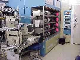

13 Analog Devices Micromachined Products Dedicated Fab >3 million accels per month, < 10 ppm QS9000 Compliant Fab, BiCMOS & MEMS


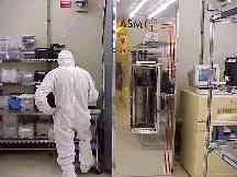
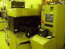
14 Processing Semiconductor Tools ETCH Photo Coat/Develop


15 Polysilicon Properties Material Properties PPM O2 Recrystallization Grain structure for 2um 580 Deg C undoped film with no O2 Cry s tal Str uc ture v s Temper ature & Depos ition Rate D e p o s itio n R a te ( A n g / m in ) Grain structure for the same deposition conditions but with O2 added to the deposition step using N2O2 mix Depos ition Temperature (de g C)

16 Sub Nanometer Coatings 0.2 nm coatings eliminate static friction Vapor deposited at wafer level for reliable films

17 Die Singulation for MEMS Protect MEMS devices with a temporary cover Up-side-down saw US Patent 5,362,681 (Analog Devices) Dicing Saw Wafer Backside Plastic Film With Holes Metal Frame Saw Kerf Wafer Die Plastic Film Without Holes Air Pocket Containing Released Microstructures

18 Dicing Exposed MEMS structures Backside Saw PVC tape punched hole MEMs area of Die Tape Seal Area Accelerometer Die
 Capabilities Better control of environment around sensor pressure & gas species Lower die stress die attach choices open")
19 Front-end Process Technology: How has imems evolved? Capping Wafer level (4 masks) Capabilities Better control of environment around sensor pressure & gas species Lower die stress die attach choices open Reliability/Quality Lower particle levels Enables lower cost packaging (i.e., plastic) foundry assembly
 Capabilities Better control of environment")

20 Front-end Process Technology: How has imems evolved? Capping Wafer level (4 masks) Capabilities Better control of environment around sensor pressure & gas species Lower die stress die attach choices open Reliability/Quality Lower particle levels Enables lower cost plastic packaging foundry assembly


21 Accelerometer Packaging Trends Package Evolution Header Xmm 10 Cerdip/Cerpa k 10 LCC QFN WSP Ymm Zmm Lead Free Packages


22 Assembly & Test Operations Subcontractor in Philippines Dedicated Line in Large Factory 200 people for accelerometers Off-Shore Manufacturing


23 Tester Development Issues to Deal With Testing Machines not Developed Measurement Standards Inadequate Dynamic Parameters and Vibration Solution Semiconductor Handler Based Tool Custom Tooling Exclusive IP Serialized Parts OCR Transfer to Off-Shore after qualification


24 Automotive Airbag Sensors < 1 ppm quality level Market Pull < 1 FIT (53 million device hours, MTBF 6.6 X 10 9 hr)

25 Inertial Sensors in Vehicles Z 6-DOF IMU Crash Detection System Satellite Sensor Airbag Dual-axis airbag sensor Seatbelt Pretensioner Low g chassis control sensor Gyro Vehicle Dynamic Control System Navigation/Driver Information System Body/Chassis Control System
26 imems Technology Accelerometers What Does an Accelerometer do? MOTION & TILT MEASUREMENT Measurement of static gravitational force e.g. Tilt and inclination Measurement of dynamic acceleration e.g. Vibration and shock measurement Inertial measurement of velocity and position Acceleration single integrated for velocity Acceleration double integrated for position
27 imems Technology F=MA Acceleration can be measured using a simple mass/spring system. Force = Mass * Acceleration Force = Displacement * Spring Constant So Displacement = Mass * Acceleration / Spring Constant Change in Displacement Add Acceleration MASS MASS
28 imems Technology Sensor Principle: Differential Capacitive Sensing Use Silicon to make the spring and mass, and add fingers to make a variable differential capacitor Measure change in displacement by measuring change in differential capacitance SPRING APPLIED ACCELERATION MASS FIXED OUTER PLATES SENSOR AT REST ANCHOR TO SUBSTRATE CS1 < CS2 RESPONDING TO AN APPLIED ACCELERATION (MOVEMENT SHOWN IS GREATLY EXAGGERATED)
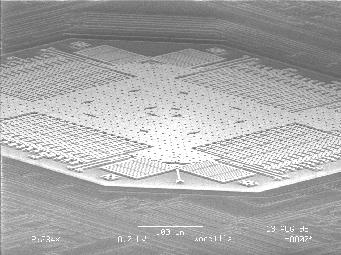
29 Integrated Micromachined Accelerometer 100 microns

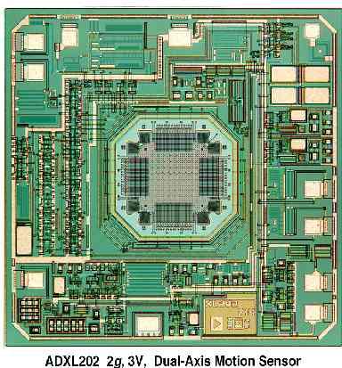
30 imems Technology Accelerometer Beam (ADXL202)

31 imems Technology Accelerometer beam (ADXL202, one corner) Center Member Etch Holes Stopper Tether, spring Self Test Fingers Anchor Fixed Fingers Moveable Fingers
32 imems Technology Amplifier Zero with adjustable gain (via thin film laser trim) g offset and sensitivity are laser trimmed at wafer level How do we trim sensitivity without shaking the part? Fn =sqrt (K/M) where K is spring s displacement vs force We measure the resonant frequency of the beam to learn the mass and spring constant Output filter Simple R-C filter for low-g products (internal R, external C) 2 pole switched capacitor filter on high-g parts

33 Early Accelerometer Design Evolution Closed Loop Tensile Spring Open Loop Folded Spring


34 ADXL78 and 278 Full Differential Designs Mechanical Design Duplicated Differential Capacitance Demodulation of Two Channels

35 Integrated Micromachined Gyro Single Chip Rate Sensor 5V Operation Std Atmosphere 150 deg per second Self-Test 0.03 deg/sec/sqrt hz Compensated 5% Single Chip Lessons Learned In Accelerometer Development of Meso Structures Detecting Nano dimensions now applied to sub picodimensions 10-3 > 10-9 > 0.01X (10 Fermi)
36 Future Trends More Integration of Circuit Functions Communications Calibration and Identification Wireless Use of Silicon-on-Insulator Preprocess the Wafer for MEMS Foundry the Semiconductor Process Use DRIE Etching to Access the Buried Oxide More Mass for Inertial Devices Handle Wafer Buried Oxide
37 SOI Sensor Configuration
38 Sensor Fabrication Process after foundry of circuits Released Structure Deep Reactive Ion Etch Stop at Buried Oxide Etch oxide beneath MEMS structures Strip Protective Photoresist

39 SOI Accelerometer Isolation Trench New Process Applied to High Volume Accelerometer

40 Trench Isolation for SOI MEMS DRIE trench etching, stopping on buried oxide Deposit dielectric lining Polysilicon refill CMP to planarize Polysilicon Refill TEOS Lining Buried Oxide

41 Integrated SOI Sensor
42 Conclusions MEMS Technology is based on microelectronics and can have similar economic advantages Surface Micromachining builds layers over a sacrifical level Inertial MEMS devices are accelerometers and gyroscopes that measure motion The trends are to smaller devices with multiple axis of sensing

43 Questions Please