How Printed Circuit Boards are Made. Todd Henninger Field Applications Engineer Midwest Region
|
|
|
- Oswin Dennis
- 5 years ago
- Views:
Transcription

1 PCB 101: How Printed Circuit Boards are Made Todd Henninger Field Applications Engineer Midwest Region
2 Tooling
 Fabrication Drawings Mechanical Dimensions Build Requirements (materials, tolerances, surface finish,")
3 PRE-PRODUCTION ENGINEERING (Tooling) Design Data Package CAD Data (ODB++ or Gerber 274x format) Independent Net List File (IPC-D-356) Fabrication Drawings Mechanical Dimensions Build Requirements (materials, tolerances, surface finish, etc.)
 IPC-6012C is main build spec Classes (1, 2, 3) Default reference specs Other series include Design")
4 INDUSTRY STANDARDS (SPECIFICATIONS) IPC (Assoc. Connecting Electronics Industries) IPC-6012C is main build spec Classes (1, 2, 3) Default reference specs Other series include Design (IPC-2221), Other series include Design (IPC-2221), Materials (IPC-4101), Test Methods (IPC- 652), etc.
 Methods")


5 PRE-PRODUCTION ENGINEERING (Tooling) Methods Engineering Material Stackup Impedance Modeling Floor Travelers CAM CAD Data Analysis and Editing Production Panelization CNC Programming Electrical Test (ET) Programming

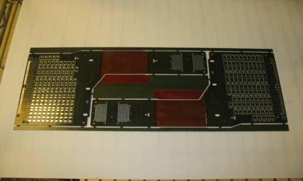


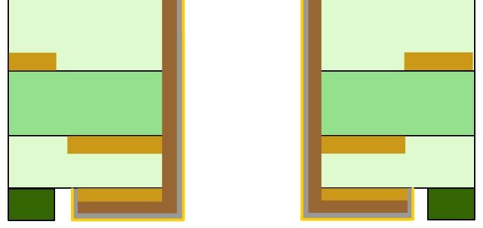
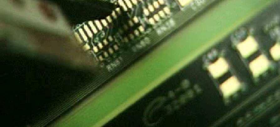
6 Assembly Sub-Panel ( Array )
7 PANEL UTILIZATION Keep-out Area Perimeter Impedance coupon PCB PCB Tooling holes Process control coupon PCB PCB Manufacturing Panel 1.0
8 PANEL UTILIZATION Very good panel utilization Poor panel utilization x x x 11.5 PCB PCB PCB x x x 11.5 PCB PCB PCB Total usable area in.^2 Total Circuit area in.^2. 98% panel utilization Total usable area in.^2 Total Circuit area in.^2. 50% panel utilization
9 PANEL UTILIZATION: Nesting Production Panel Size Usable Area No Nesting Panel Yield = 6 parts Circuits Nested Panel Yield = 8 parts Optimized Nesting Panel Yield =10 parts Part folded to shape after punching

10 PCB Materials
 or 1oz (1.2 mils) Dielectric: Thickness Ranges.002 -.")

11 Core: PCB Building Block Copper Foil: Typical Thickness 1/2oz (0.6 mils) or 1oz (1.2 mils) Dielectric: Thickness Ranges or greater Glass Bundles & Organic Resin ( FR4 ) or high-performance specialty material (Teflon, Ceramic, Polyimide, Low-Df, etc.)
")

12 FR4 Woven Glass Styles Glass Style: 106 Plain Weave Count: 56x56 (ends/in) Thickness: Glass Style: 1080 Plain Weave Count: 60x47 (ends/in) Thickness: Source: Isola
")

13 FR4 Woven Glass Styles Glass Style: 2113 Plain Weave Count: 60x56 (ends/in) Thickness: Glass Style: 2116 Plain Weave Count: 60x58 (ends/in) Thickness: Source: Isola
 Thickness:")
 Thickness: 0.")
14 FR4 Woven Glass Styles Glass Style: 1652 Plain Weave Count: 52x52 (ends/in) Thickness: Glass Style: 7628 Plain Weave Count: 44x32 (ends/in) Thickness: (in) Source: Isola
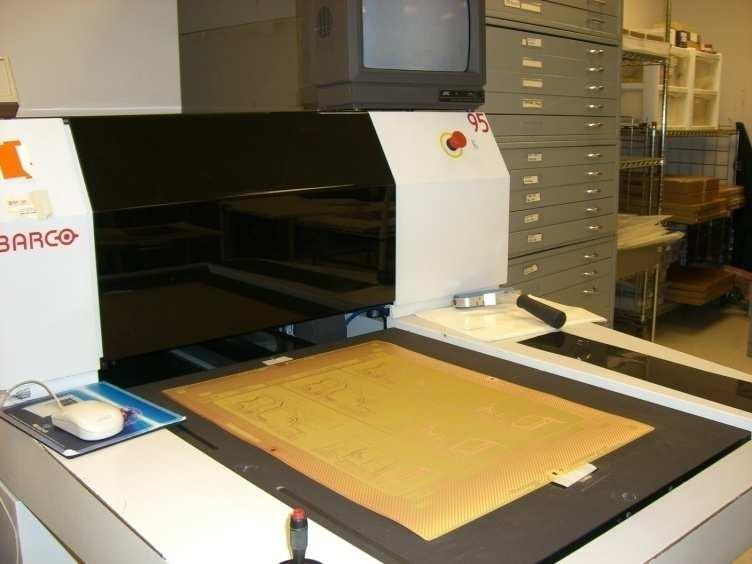
15 Production Processes


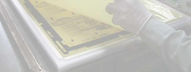
16 INNER LAYER PRINT AND EXPOSE Expose Copper clad laminate Photo-tool Photo-resist Copper foil Dielectric

17 Laser Direct Imaging (LDI) Elimination of Photo Tools No Film/Artwork Movement Quick Turn Made Easy Run product as soon as Engineering releases data to the floor Reduction in Defect Count Direct Write = No Film related defects No issues related to loss of vacuum Improved Resolution System Resolution 4000 dpi Current process capability ( / ) CCD Camera System & Target Fiducials Positional Accuracy +/-25µm (.001 ) Scanning Optics


18 DEVELOP Copper clad laminate Photo-resist Copper foil Dielectric


19 COPPER ETCH


20 RESIST STRIP


21 AUTOMATED OPTICAL INSPECTION (AOI) & OXIDE Oxide

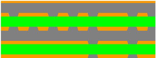
22 LAYUP Foil Prepreg Core Prepreg Core Prepreg Core Prepreg Foil
23 Stackup Example
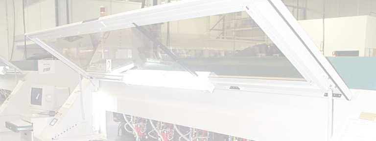
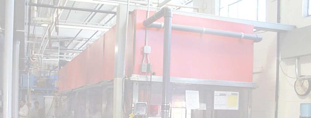
24 LAMINATION
25 LAMINATION


26 LAMINATION
27 MECHANICAL DRILL


28 MECHANICAL DRILL
29 Small Diameter Mechanical Drills Human hair 2.5 mil (60 micron) to 3.5 mil (90 micron) Small diameter are very fragile 5.9 mil (150 micron) High speed spindles are required Feed rates are about 50% of standard via diameters Drill life of 300 to 600 hits depending on material Short flute length limits hole depth Drill cost is higher Carbide drill bit
30 Via Structures: Thru-Hole, Blind, Buried Stacked microvia Stacked microvia using a microvia in the sub-lamination Offset via Through via Sub-Lamination Layer 1 Layer 2 Layer 3 Layer 4 Layer 5 Layer 6 Layer 7 Layer 8 Prepreg Prepreg Prepreg Laminate Core Prepreg Laminate Core Prepreg Laminate Core Prepreg Prepreg Prepreg Layer +2 Layer +1 Layer +1 Layer +2


31 MICROVIAS: DRIVEN BY TIGHT SPACING Q2 Q1 Q3 Q4 L1 L2 L3 L4 L5 L6


32 LASER DRILLING: MICROVIAS UV To cut copper
33 LASER DRILLING: MICROVIAS CO2 To cut dielectric material


34 LASER DRILLING: MICROVIAS U.V. drilling of copper using focused, spiraling beam CO2 drilling of laminate dielectric using refracted beam
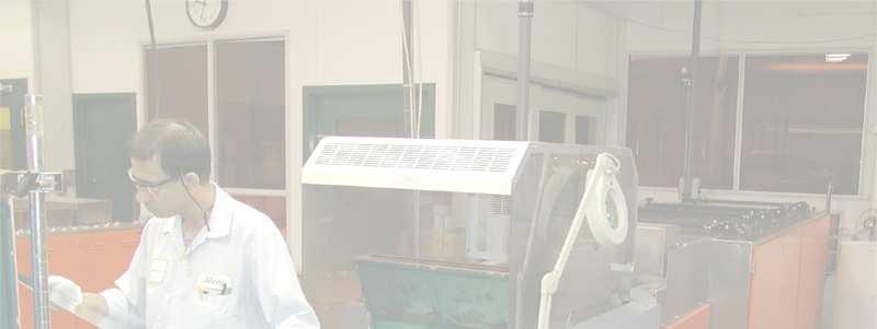
35 DESMEAR: PLASMA OR CHEMICAL
36 HOLE PREPARATION As Drilled
37 HOLE PREPARATION After Desmear
38 HOLE PREPARATION Laser Microvia Post-Desmear


39 ETCHBACK
40 Hole Fill: Via-in-Pad Conductive Via fill Non-conductive Via fill
41 Via Hole Fill Equipment Vacuum Assist Via Filling
42 Automated Linear Surface Grinder Excess (Cured) Fill Material Removed


43 Microvia Copper Fill Planar Microvia dia. Stacked Microvia Layer 1 Layer 2 Layer 3 Brightener Carrier Source: Capture pad

44 ELECTROLESS COPPER


45 OUTERLAYER IMAGE Expose Photo-tool Photo-resist

46 DEVELOP
47 ELECTROLYTIC COPPER PLATE


48 ELECTROLYTIC COPPER PLATE

")
49 TEMPORARY TIN PLATE (ETCH RESIST)

50 STRIP PHOTO RESIST


51 COPPER ETCH
52 COPPER ETCH Base copper Plated copper E less copper Laminate
53 COPPER ETCH
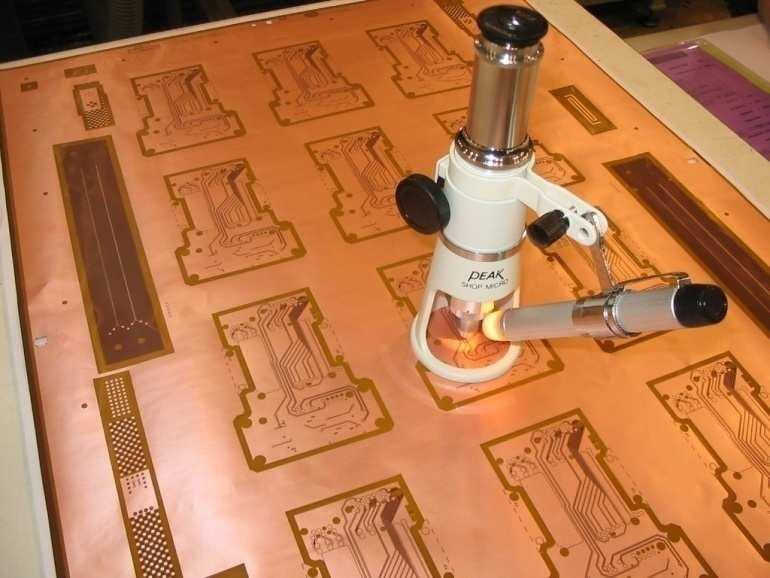
54 COPPER ETCH
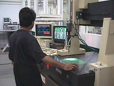
55 COPPER ETCH
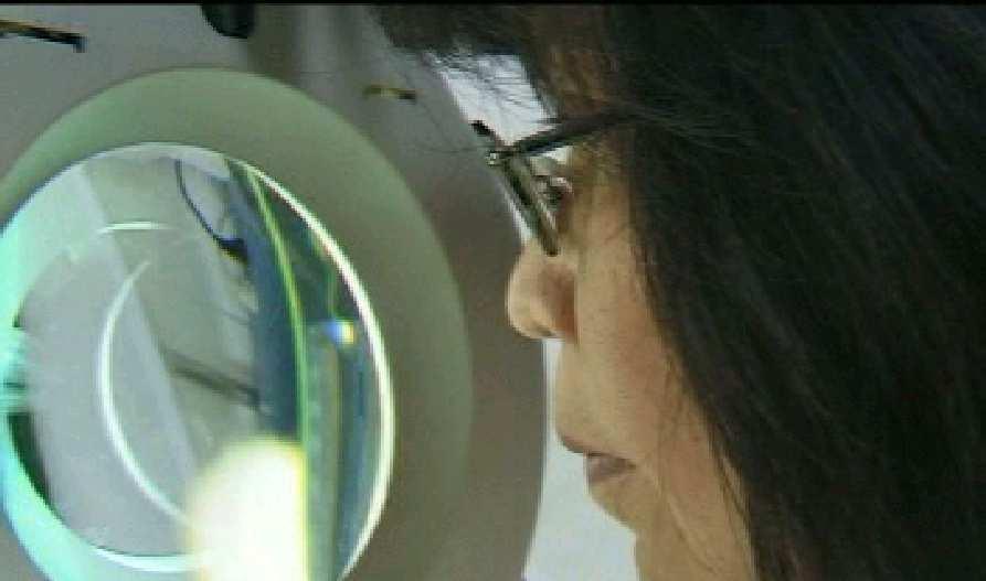
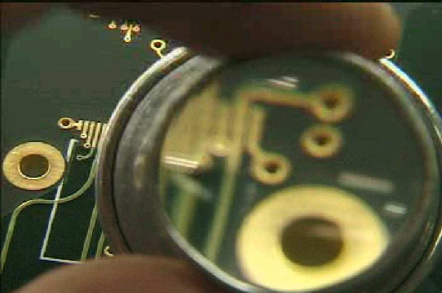
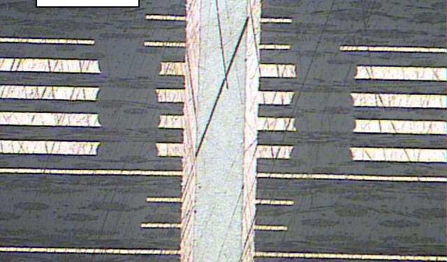
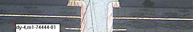
56 COPPER ETCH
57 COPPER ETCH
58 COPPER ETCH

59 TIN RESIST STRIP


60 LIQUID PHOTO IMAGABLE (LPI) SOLDERMASK APPLICATION


61 EXPOSE Expose Photo-tool

62 DEVELOP
63 SOLDERMASK DEVELOP

64 SOLDERMASK TENTING


65 SOLDERMASK TENTING Clearanced ( Encroached ) Tented


66 FINAL SURFACE FINISH (ENIG EXAMPLE)

67 SILKSCREEN NOMENCLATURE


68 AUTO ROUT (DEPANELIZATION)


69 ELECTRICAL TEST 1) CLAMSHELL ( BED OF NAILS ) 2) FLYING PROBE

70 VISUAL INSPECTION / PIN GAUGE

71 DIMENSIONAL VERIFICATION


72 MICROSECTION


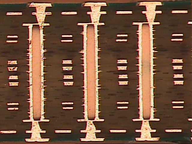
73 Annular Ring IPC 6012B Class 2 IPC 6012B Class 3 Minimum annular Ring mil Larger pad than Class II to allow For registration 90 degree Breakout Minimum annular Ring mil Worst case registration allowed by IPC Class II Worst case registration allowed by IPC Class III
74 TDR (Impedance Verification)
 Developed by")

75 Interconnect Stress Test (IST) Developed by PWB Interconnect Solutions Inc. (

76 PACK & SHIP
77 QUESTIONS? THANK YOU Todd Henninger Field Applications Engineer Midwest Region