MEMS/NEMS towards smart systems integration
|
|
|
- Amy Jenkins
- 5 years ago
- Views:
Transcription

 at Chemnitz University of Technology WPI, Tohoku")
1 MEMS/NEMS towards smart systems integration Prof. Dr. Thomas Gessner Fraunhofer Research Institution for Electronic Nano Systems ENAS Center for Microtechnologies (ZfM) at Chemnitz University of Technology WPI, Tohoku University Sendai Page 1
2 OUTLINE 1. Introduction /ZfM 2. International trends in SSI 3. NEMS/MEMS and System Examples 4. Conclusions Page 2

3 Smart Systems Campus Chemnitz TUC, application lab 3D-Micromac AG Start-up-building Page 3 TUC, ZfM


4 University of Technology, Chemnitz Basic Research Applied Research Page 4

5 Fraunhofer Research Institution for Electronic Nano Systems MEMS/NEMS Design Development of MEMS/NEMS MEMS/NEMS Test System Packaging / Waferbonding in Chemnitz International Offices: Since 2001 / 2005 Tokyo/Sendai-Japan Since 2002 Shanghai-China Since 2007 Manaus-Brazil Back-End-of-Line Technologies for Micro- and Nanoelectronics Process and Equipment Simulation Micro and Nano Reliability Printed Functionalities Advanced System Engineering Page 5


6 / ZfM A look behind the doors of the clean room facilities Page 6
7 OUTLINE 1. Introduction /ZfM 2. International Trends in SSI 3. NEMS/MEMS and System Examples 4. Conclusions Page 7

8 More than Moore / Smart Systems Page 8


, that bridges the Gap between")
9 Definition Smart Systems Integration Integration of Different Functionalities such as Signal Processing, Sensors, Actuators, Photonics, Power, Coolers with a High Degree of Miniaturisation and Flexibility to Reasonable Costs in one Unit (e.g. Package), that bridges the Gap between Nano-Electronics and Application Page 9
10 Smart Systems Integration & Packaging MEMS / NEMS Electronic Components Communication Unit Processor & Memory Power Radio Sensor & Actuator CMOS Microsystem technologies Hetero system integration Page 10
11 Local Personal Network Smart Glasses Smart Briefcase Smart Cards Smart Watch Smart Shoe Personal Communicator Page 11


")


12 Internet of Things - anywhere Home Office Car Industry Shops Street Hotels Hospital Ski Slope Internet of Things (IoT) smart objects wireless communication broad band internet Page 12
13 OUTLINE 1. Introduction /ZfM 2. International trends in SSI 3. NEMS/MEMS and System Examples 4. Conclusions Page 13

14 RFID Applications Material Tracing Box Management Facility Management - Quelle: ITM/Ruhr-Universität -Bochum Quelle: ITM/Ruhr-Universität -Bochum Quelle: ITM/Ruhr-Universität -Bochum RFID Application with Complex Additional Functions Detection of temperature acceleration pressure - light Combination of display and RFID Data processing and storage partly on the label Page 14


 shock")


15 Conventional Sytems Type of transport monitoring sensor: adhesive label (mechanical / chemical) shock sensor tilt sensor temperature sensor humidity sensor Type of transport monitoring sensor: electronic measurement system Page 15
 label for the monitoring of shock, inclination and temperature during transportation processes Partner: KSW Microtec AG ELMOS")
16 Project ASIL: Active Smart ID Label BMBF collaborative project: priority topic of the Microsystems framework programme: Microsystems Technology for Smart Label Applications in Logistics Objective: development of an active radio frequency identification (RFID) label for the monitoring of shock, inclination and temperature during transportation processes Partner: KSW Microtec AG ELMOS Semiconductor AG Schenker AG Memsfab GmbH TUC-ZfM/ Page 16
17 Project ASIL- RFID label concept The label components: - RF-chip with antenna - battery for energy supply - sensor system consisting of the micromechanical transducer and the signal processing electronic The system has to detect and record inclination and mechanical shock. In order to reduce the complexity of the system, it is reasonable to measure both with the same microstructure. KSW Microtec Smart RFID label Interposer Battery ELMOS Signal Processing A/D Conversion ASIC-Chip Temperature Sensor KSW Microtec Logic / Memory RFID-Chip TUC-ZfM/Memsfab Shock Sensing Inclination Sensing MEMS-Chip Submodule RF- Front End Antenna Specific requirements for the sensor system: - low energy consumption - high signal to noise ratio - high temperature stability - low device / sensor thickness Page 17


18 Concept of the sensor system Capacitive MEMS Transducer ( Air gap Insulation of Microstructures) HARMS High Aspect Ratio Microstructure four mask level technology high capacitive sensitivity low parasitic capacitance small thermal sensitivity low manufacturing costs Page 18
 Sensor driving and signal processing C to V conversion signal filtering, A/D conversion and")
 Energy saving communication")
19 Concept of the sensor system Ultra low power sensor ASIC (M by ELMOS Semiconductor AG) Sensor driving and signal processing C to V conversion signal filtering, A/D conversion and data storage controlling of logical sequence and time cycle communication with RFID-ASIC low power management Energy efficiency ultra low power design energy saving measurement cycle (variable power down phase) Energy saving communication phase (event-driven [threshold] or external requested [polling mode]) Page 19


20 Packaging and Assembly Concept Fabrication technology: Roll to roll fabrication demands flexibility of the layers Overall thickness of the label is limited Restricted chip height Page 20


21 Inclination sensor in AIM technology Sensitive gap 0.6 µm µm trench depth Page 21


22 Vibration sensors Frequency Selective Tunable Vibration Sensor Page 22 Structure born noise detection Monitoring of machines, engines and tools Pump monitoring Switch off your system before demolition fraction of: shafts, bearings, etc. danger of life?
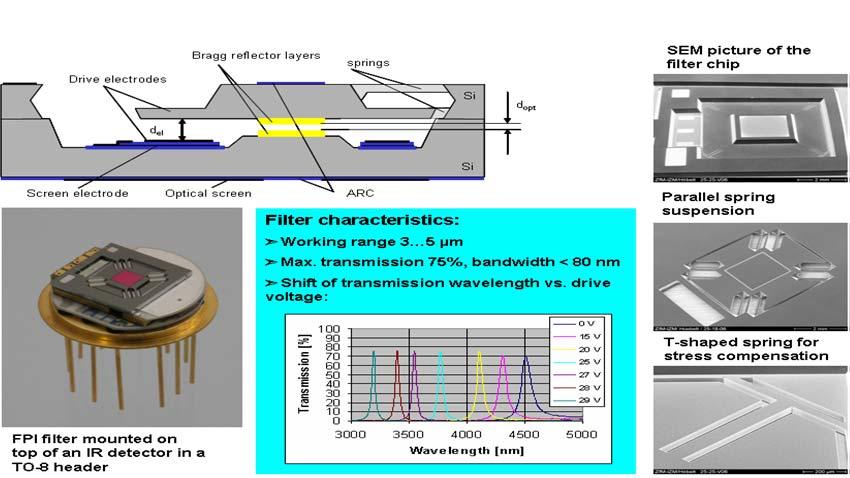
23 Fabry-Perot-Interferometer (FPI) Page 23


 Cooperation of ZfM, and IZM")

24 MEMS RF switch DC-4 4 GHz, 10 µs s switching time Research project by order of Sony, Tokyo Extremely high requirements (concerning supply voltage & switching time, switching time only 1/10 of competitive products, life cycle 1 Billion cycles) Cooperation of ZfM, and IZM (HDI&WLP) MEMS manufacturing Chip layout Modeling and Simulation of mechanical behaviour Field calculation Page 24
 Lateral arrangement and small distances between the electrodes <1 µm lead to")
 RF current path in on state: Push rod electrostatically actuated by 5 Volt Page")
25 MEMS RF switch DC-4 GHz, 10 µs switching time Special layout in the contact area to ensure RF isolation (-35 db) Lateral arrangement and small distances between the electrodes <1 µm lead to large contact forces (reliability) Hermetic Wafer Level Packaging allows fast switching (10 µs, no air damping) RF current path in on state: Push rod electrostatically actuated by 5 Volt Page 25
26 MEMS to NEMS - challenges Limitation of material properties of very thin ( nm range) movable elements Technology issues by the fabrication of mechanical part in the nm range New integration technolgies are necessary New device and material strategy must be developed Page 26


27 In-Process Sensing Gap Reduction of Capacitive Transducers Principle Fabrication Process The in-process trench width reduction is based on the displacement of a substructure actuated by a buckling beam mechanism. The displacement is exited by compressive stress which yields a longitudinal force in the acting beams and hence the buckling. The substructure is moved and fixed against a predefined stop by the stress-induced force in the beams. Page 27


![10000 Frequency [Hz] new principle after displacing Gap](/docs-images/90/102610470/images/28-2.jpg "width down to < 100 nm for increased sensitivity of")
28 In-Process Sensing Gap Reduction of Capacitive Transducers before - Output voltage [mv rm s ] Sensitive gap 0.6 µm µm trench depth reference structure Frequency [Hz] new principle after displacing Gap width down to < 100 nm for increased sensitivity of shrinking devices Page 28
29 & TU Chemnitz / ZfM Nanoelectronics Ultrathin Films Nanomaterials Nano Devices Nano Systems - Process, Material & Technology Development Porous ULK dielectrics Cu interconnect scaling - PVD -CVD -ALD diffusion barriers metal films for seed layers, electrodes etc. - Nano composits (Polymer based) - Nano laminates - Carbon Nano Tubes (CNT) - Nano wires - Nanofunctionalities - Design - Technology -> NEMS Airgap structures catalyst / nanoparticles for CNT growth TU Chemnitz: * Institute of Physics * Institute of Chemistry Networking: *Nano-CC Ultrathin Films led by Fraunhofer-IWS Dresden *ENIAC: European Nanoelectronics Initiative *Fraunhofer Nanotechnology Alliance Page 29
: - Fast heating rate: up to 10 9 K/s Si - High reaction speed: up to 30 m/s")
 First bond tests with Al/Ni foils Si TEM micrograph of Al/Ti")
30 Bonding with nanostructured multi layers -NANOBOND- Target: Using nanostructured multilayer as internal heat source for wafer bonding 3D-Integration Self-propagating high-temperature synthesis (SHS): - Fast heating rate: up to 10 9 K/s Si - High reaction speed: up to 30 m/s Hundreds/thousands of nanoscale layers ( nm) which react exothermically during intermixing Conventionally used as freestanding macroscopic foils First patents applied at ENAS (deposition and structuring) First bond tests with Al/Ni foils Si TEM micrograph of Al/Ti multilayer Page 30

The promotion of applied research projects on materials and system architecture that will")

31 WPI-AIMR In addition to basic research, WPI-AIMR is committed to pursuing (1)The creation of new compounds and materials with innovative functions which exceed existing ones. (2)The construction of devices based upon a new fundamental paradigm. (3)The promotion of applied research projects on materials and system architecture that will generate direct societal impacts. In addition, WPI-AIMR is committed to establishing innovations in understanding diverse material functions through the creation of new basic materials and compounds which brings significant benefits for the future of humanity. Page 31

32 Gessner Lab in Tohoku University Starting: November 1, 2008 Assistant Prof. Yu-Ching Lin Affiliation: WPI-AIMR, Tohoku University World Premier International Institute for Materials Research, Tohoku University, Sendai Japan Location: Esashi Laboratory MNC (Micro/Nano-Machining Research and Education Center), Aobayama campus of Tohoku University Research associates and students joined in Page 32
, Aobayama")
 Integrated material (i)")
 Inductor(integrate with nano -material) nano -Material (nano ferrite) LTCC (integrated passives) LSI LTCC with integrated")
33 Gessner Lab in Tohoku University Started: November 1, 2008 Affiliation: WPI-AIMR, Tohoku University World Premier International Institute for Materials Research, Tohoku University, Sendai Japan Location: Esashi Laboratory MNC (Micro/Nano-Machining Research and Education Center), Aobayama campus of Tohoku University Nano structure wafer bonding Metallic glass bonding MEMS with new functional materials Reactive Multilayer Silicon Al Ti Reactive multi layers Nano porous metal Zr 258 Kcal/mol Ti O 205 Kcal/mol Si Metallic glass Ti Zr O Si Si O 218 Kcal/mol (ii) Integrated material (i) Molded metallic glass (iii) Bonded substrate Micro mirror made from metalic glass Cover ( integrate with antenna) (LTCC/Glass/Si) NEMS (variable EDLC with carbon nano tubes) Inductor(integrate with nano -material) nano -Material (nano ferrite) LTCC (integrated passives) LSI LTCC with integrated RF-Components Page 33


34 Carbon Nanotubes as Via Material in IC CNT growth with thermal CVD Development of an integration process compatible with the microelectronics baseline 500 nm Source: TU Chemnitz Multi wall carbon nanotubes grown with C 2 H 4 precursor on Ni-catalyst at 665 C A challenge for characterization and measurement a new approach for a reliability strategy necessary Page 34

 603 Micro and Nanosystems ETH Zurich Source: Stampfer et al. Nano Lett.")
35 Sensor based on Carbon Nanotubes (CNT) CNT are very promising structures for the further miniaturization of sensors due to their unique properties SEM image of a SWNT SEM image of cantilever CNT sensors in research SWNT-based sensing device pressure sensors force Infineon sensor displacement sensor infrared sensors gas sensors Source: Jungen et al. J. Micromech. Microeng. 17 (2007) 603 Micro and Nanosystems ETH Zurich Source: Stampfer et al. Nano Lett. Vol 6 No Micro and Nanosystems ETH Zurich Page 35


36 CNT ZfM / ENAS CNT Deposition with Dielectrophoresis CNT Growth with CVD High quality SWNTs and MWNTs 3D - Alignment Low temperature process Direct growth of high density CNTfilms 3D Alignment with DC - field Selflimiting Dense vertical alignment 3D alignment and wiring Via interconnects 10 µm Sensors Actuators 5 µm NEMS Page 36


37 CNT ZfM / ENAS CNTs for low temperature flip chip connections CVD - Reactor Si/ SiO 2 Cu TiN Ni/ CNT Contact pad Chip Ni - Pad Electrical characterization Raman and TEM studies MWNT CoNTemp -project MWNT with 16 shells Page 37
38 OUTLINE 1. Introduction /ZfM 2. International trends in SSI 3. NEMS/MEMS and System Examples 4. Conclusions Page 38
39 Conclusions Smart System Integration will be a future tendency Many products (prototypes) and technologies were developed in the field of Microelectronics and MEMS Future trends are increasing functionality in one system at the same time with degreasing size (NEMS) Complex system integration needs advanced packaging methods Page 39
40 Future Challenges Nanotechnologies and Devices Smart Systems Integration Page 40

41 European Conference & Exhibition on integration issues of miniaturized systems MEMS MOEMS, ICs and electronic components 1. Conference : March 2007, Paris 2. Conference: April 2008, Barcelona 3. Conference: March 2009, Brussels 4. Conference: March 2010, Milano/Como Organizer: Part of the activities of: Page 41