Challenges of Smart Systems Integration
|
|
|
- Lindsey Matthews
- 5 years ago
- Views:
Transcription
1 Challenges of Smart Systems Integration Prof. Dr. Thomas Gessner Fraunhofer Research Institution for Electronic Nano Systems ENAS Center for Microtechnologies (ZfM) at Chemnitz University of Technology WPI, Tohoku University Sendai Page 1
2 Fraunhofer-Gesellschaft in Germany Itzehoe Lübeck Rostock 57 Institutes at 40 locations Bremen Hannover Berlin Potsdam Paderborn Chemnitz Teltow Braunschweig Nuthetal Magdeburg Oberhausen Paderborn Cottbus Dortmund Halle Schmallenberg Leipzig Schkopau Duisburg Dresden Sankt Augustin Aachen Ilmenau Jena Euskirchen Chemnitz Darmstadt Würzburg Kaiserslautern Erlangen Wertheim St. Ingbert Saarbrücken Pfinztal Nürnberg Karlsruhe Stuttgart Freising Freiburg München Efringen-Kirchen Holzkirchen Page 2


3 Smart Systems Campus Chemnitz 3D-Micromac AG CUT, Lightweight Structures Engineering Start-up building CUT, Institute of Physics and ZfM Page 3

4 Fraunhofer Research Institution for Electronic Nano Systems ENAS MEMS/NEMS Design Development of MEMS/NEMS MEMS/NEMS Test System Packaging / Waferbonding Back-End-of-Line Technologies for Micro- and Nanoelectronics in Chemnitz International Offices: Since 2001 / 2005 Tokyo/Sendai-Japan Since 2002 Shanghai-China Since 2007 Manaus-Brazil Process and Equipment Simulation Micro and Nano Reliability Printed Functionalities Advanced System Engineering Page 4
5 Content International Trends Smart Systems for different Applications Smart Label Fabry-Perot Interferometer Laser micromachining for different applications Summary and Conclusions Page 5

6 More than Moore / Smart Systems Page 6

, that bridges the Gap between Nano-Electronics and Application")
7 Definition Smart Systems Integration Integration of Different Functionalities such as Signal Processing, Sensors, Actuators, Photonics, Power, Coolers with a High Degree of Miniaturisation and Flexibility to Reasonable Costs in one Unit (e.g. Package), that bridges the Gap between Nano-Electronics and Application Page 7
8 Smart Systems Integration & Packaging MEMS / NEMS Electronic Components Communication Unit Processor & Memory Power Radio Sensor & Actuator CMOS Microsystem technologies Hetero system integration Page 8
9 Content International Trends Smart Systems for different applications Smart Label Fabry-Perot Interferometer Laser micromachining for different applications Summary and Conclusions Page 9

10 RFID Applications Material Tracing Box Management Facility Management - Quelle: ITM/Ruhr-Universität -Bochum Quelle: ITM/Ruhr-Universität -Bochum Quelle: ITM/Ruhr-Universität -Bochum RFID Application with Complex Additional Functions Detection of temperature acceleration pressure - light Combination of display and RFID Data processing and storage partly on the label Page 10
 label for the monitoring of shock, inclination and temperature during transportation processes Partner: KSW Microtec AG ELMOS")
11 Project ASIL: Active Smart ID Label BMBF collaborative project: priority topic of the Microsystems framework programme: Microsystems Technology for Smart Label Applications in Logistics Objective: development of an active radio frequency identification (RFID) label for the monitoring of shock, inclination and temperature during transportation processes Partner: KSW Microtec AG ELMOS Semiconductor AG Schenker AG Memsfab GmbH TUC-ZfM/ Page 11
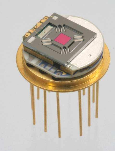
12 Project ASIL- RFID label concept The label components: - RF-chip with antenna - battery for energy supply - sensor system consisting of the micromechanical transducer and the signal processing electronic The system has to detect and record inclination and mechanical shock. In order to reduce the complexity of the system, it is reasonable to measure both with the same microstructure. KSW Microtec Battery Interposer ELMOS Signal Processing A/D Conversion ASIC-Chip Temperature Sensor KSW Microtec Logic / Memory RFID-Chip Smart RFID label TUC-ZfM/Memsfab Shock Sensing Inclination Sensing MEMS-Chip Submodule RF- Front End Antenna Specific requirements for the sensor system: - low energy consumption - high signal to noise ratio - high temperature stability - low device / sensor thickness Page 12


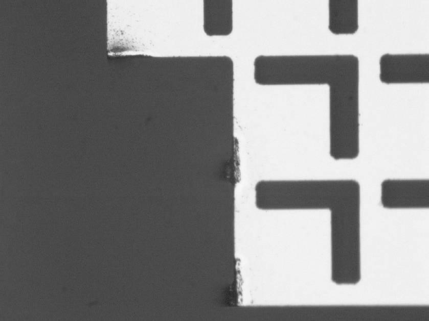
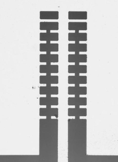
13 Concept of the sensor system Capacitive MEMS Transducer ( Air gap Insulation of Microstructures) HARMS High Aspect Ratio Microstructure four mask level technology high capacitive sensitivity low parasitic capacitance small thermal sensitivity low manufacturing costs Page 13


14 Packaging and Assembly Concept Fabrication technology: Roll to roll fabrication demands flexibility of the layers Overall thickness of the label is limited Restricted chip height Page 14
15 Content International Trends Examples of MEMS Devices for RF and Optical Applications Smart Label Fabry-Perot Interferometer Laser micromachining for different applications Summary and Conclusions Page 15
 Application: Page 16")
16 Fabry-Perot-Interferometer (FPI) Application: Page 16
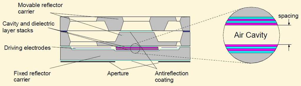
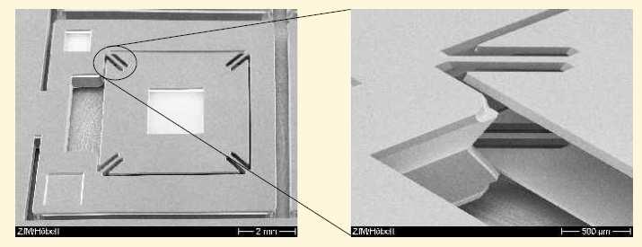
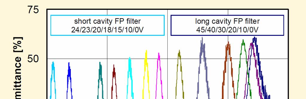
17 Fabry-Perot-Interferometer (FPI) Cross section of FPI filter chip SEM images showing the movable reflector and elastic suspension Transmission curves Page 17
18 Content International Trends Examples of MEMS Devices for RF and Optical Applications Smart Label Fabry-Perot Interferometer Laser micromaching for different applications Micro mirrors for spectrometer Microfluidic cartridges Summary and Conclusions Page 18
19 MEMS-spectrometer MEMS spectrometers enable realizing smart systems to supplement or replace traditional technology for particular demands Miniaturization and Portability Flexibility Cost efficiency Properties Configurable in wavelength range µm High wavelength repeatability ( < 0.1nm ) High sensitivity (SNR > 7.000:1) Fast measuring time (2ms) > enables real time measurements Flexible measurement setups (ATR, diffuse reflection, transmission) Page 19


20 Laser trimming of silicon micro mirror devices Spring stiffness trimming elements Mass trimming elements Cutting of mass trimming elements Mass trimming elements Spring stiffness trimming elements cutting of the spring bar stiffeners Page 20

21 Smart Systems for Molecular Diagnostics: Future needs and perspectives Smart Systems for Molecular Diagnostics in Point-of-Need Applications: Integrated platforms that provide the entire sample processing chain from Sample Taking and Preparation to Data Processing, Storage and Communication. (Source: / EPoSS SRA) Page 21
 (based on Frost & Sullivan: US Microfluidics/ Lab-on-a-Chip markets, 2008) It is well-established [ ] that analysis can be miniaturised onto a")
22 Microfluidics for Diagnostics - Markets Increasing market for microfluidics in diagnostics / Lab-on-a-Chip : European Lab-on-chip and Microfluidics Market US Lab-on-chip and Microfluidics Market (Frost & Sullivan: European Lab-on-a-Chip markets, 2009) (based on Frost & Sullivan: US Microfluidics/ Lab-on-a-Chip markets, 2008) It is well-established [ ] that analysis can be miniaturised onto a chip. However, the real challenge is to miniaturise [ ] important features such as fluid handling [ ] (Frost & Sullivan: European Lab-on-a-Chip markets, 2009) If biosensors were cars, microfluidics would be the roads Page 22
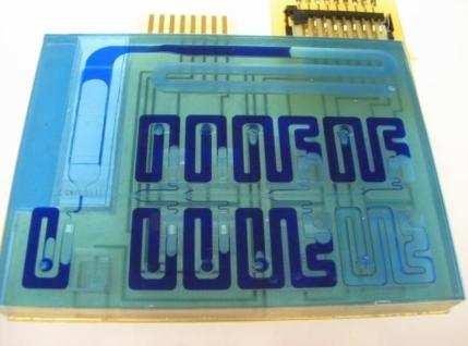
23 Microfluidic lab-on-a-chip Fraunhofer biosensor microfluidics Integration Complete microfluidic cartridge with sensor for fluorescence detection Page 23


24 Bio sensing based on NEMS optical sensors 1 Sensing layer: SPR sensor with waveguides: Multi layer stack based on Au or Ag, thickness < 150 nm molecules Sensing layer system waveguide Phase matching of waveguide mode and plasmon mode Transmission n1 n2 substrate wavelength Sensing principle: Surface plasmon resonance at a metal-dielectric interface Light projected to the surface interacts with the plasma waves Absorption peak depending on the refractive index Refractive index changes due to bio molecules attached to the surface Page 24


25 Bio sensing based on NEMS optical sensors 2 TIRF sensor with coupling prisms: TIRF=total internal reflection fluorescence Sensor slide fabrication by polymer hot embossing Page 25
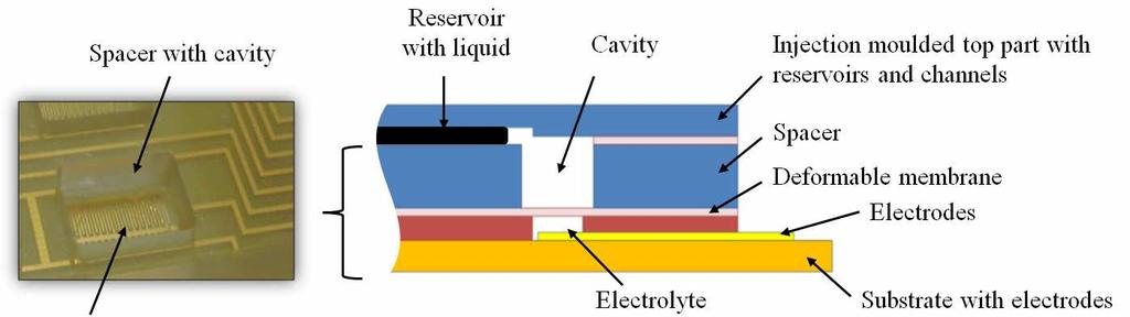
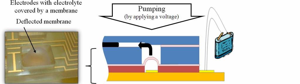
26 Low-cost integrated micropumps working principle Page 26
 Complete microfluidic cartridge with")

27 Integration (Microfluidics + SPR/Fluorescence + bio) Complete microfluidic cartridge with SPR sensor Complete microfluidic cartridge with TIRF sensor for fluorescence detection Page 27
28 Complexity of design and fabrication process chain Biomarkers Fabrication of reagents Readout system fabr. Assay (lab scale) Preparatio n Software LoC design Substrate Assembly Functional Layer On-Chip Chemicals Sensor Integration Assembly Readout Surface modification Active component s Blocking Replication technology Integrated electronics Spotting Sensor fabrication Example from the Fraunhofer ivd-platform ( Page 28 Fraunhofer in vitro Diagnostik-Plattform
29 Content Research Activities of International Trends Examples of MEMS Devices for RF and Optical Applications Smart Label Wideband Vibration Sensors for Condition Monitoring Fabry-Perot Interferometer RF Microcoils for Nuclear Magnetic Resonance Spectroscopy, RF-MEMS Varactors for Adaptive Impedance Matching Summary and Conclusions Page 29
30 Conclusions Many products (prototypes) and technologies were developed and transferred in the field of Microelectronics and MEMS Future trends are increasing functionality in one system at the same time with degreasing size Complex system integration needs advanced packaging methods Page 30


31 European Conference & Exhibition on integration issues of miniaturized systems MEMS MOEMS, ICs and electronic components 1. Conference : March 2007, Paris 2. Conference: April 2008, Barcelona 3. Conference: March 2009, Brussels 4. Conference: March 2010, Milano/Como 5. Conference: April 2011, Dresden Organizer: Part of the activities of: Page 31