FEI Materials Science Driving Discovery Through Innovative Solutions
|
|
|
- Melvyn O’Brien’
- 5 years ago
- Views:
Transcription


1 FEI Materials Science Driving Discovery Through Innovative Solutions
2 Explore. Discover. Resolve.
3 Innovative materials play essential roles in safety, clean energy, transportation, human health, and industrial productivity. Whether exploring alternative energy sources or developing stronger, lighter materials and sophisticated nanodevices scientists turn to FEI to help them find answers. Our solutions offer vast exploration and experimentation capabilities. Our expertise helps refine materials imaging, analysis, and characterization. As a result, customers have scaled new heights of discovery and recognition, and a few have even won the Nobel Prize. Driving Discovery Through Innovative Solutions FEI 1

4 As Challenges Grow Larger, Answers Become More Critical According to the European Commission, 70 percent of all technical innovations are directly or indirectly linked to materials. To fuel continued innovation, researchers want to deepen their understanding of the physical and chemical properties of materials morphological, structural, magnetic, thermal, and mechanical at macro-, micro-, and nanoscales. There are hundreds of reasons to improve the value, life span, strength, and plasticity of materials. For example, metals are integral to generating clean steel products and wind and water power; increasing strength and fuel efficiency of transportation, aerospace, and heavy equipment; and developing innovative instruments and tools for medicine, construction, and other industries. In the fields where new polymer and catalyst systems are being developed, chemists and chemical engineers want to better understand the relationships between materials structures and their functional properties on the micro- and nanometer scales. Their discoveries lead to new materials systems with targeted functionality, longer active lifetimes, lower replacement costs, improved strength, and better manufacturability. The exciting field of nanodevices is focused on developing miniaturized devices with specific functionality for electronic, magnetic, mechanical, and optical systems. Sensors, actuators, and microfluidic devices are in high demand to help solve global energy, communications, and critical monitoring challenges. As scientists expand their knowledge of material structures, they also want to understand how materials behave in response to light, heat, cold, pressure, and other stimuli. And two-dimensional answers do not always yield answers in a threedimensional world. Imaging, analysis, and materials characterization must deliver real-world visibility. 2 FEI Explore. Discover. Resolve.

5 Visualization of the differential phase contrast of GaN showing the local electrostatic fields on the atomic level. Image courtesy of Prof. J. Zweck, Physics department, University of Regensburg, Germany. Driving Discovery Through Innovative Solutions FEI 3

6 Microstructure is critical in affecting material performance, and microscopy is key to the evaluation and characterisation of materials. The Titan with ChemiSTEM technology is giving us a new window into the structure and composition of materials, helping us understand how materials perform. With this unique perspective, we can work to develop ways to predict performance under different environmental conditions and engineer materials to have longer lifetimes. Dr. Grace Burke, Director, Materials Performance Center & Electron Microscopy Center, Manchester University

7 Transforming Insight into Innovation The intellectual property and insight resulting from materials science research help enhance researchers ability to successfully correlate structural properties with functional performance. In turn, this insight helps commercial enterprises innovate products and processes to gain important time-to-market and cost advantages. Moving from insight to innovation poses a series of challenges unique to materials science. Materials can be hard or soft, delicate or durable, thin or thick, organic or inorganic, conductive or nonconductive. This incredible variation makes sample preparation challenging. At the same time, researchers need to obtain accurate characterization data without affecting the sample itself. When investigating multiple combined factors, the associated challenges can multiply almost exponentially. Materials diversity also complicates imaging, which can affect workflow and results. Two-dimensional visualization is standard, but scientists must also be able to see how material composition affects function in a three-dimensional world. Nanometer and sub-nanometer visibility has become a requirement, regardless of sample type. Finally, materials samples are not static. Understanding how they react under environmental influences is crucial to develop new materials and improve their application. Scientists want to visualize changes as they occur at the micro-, nano-, or atomic scales in real time. Simplifying sample preparation, imaging, analysis, and visualization workflow demands in-depth understanding of the challenges of each step and real solutions. Driving Discovery Through Innovative Solutions FEI 5
8 Want to learn more? FEI.com/materials-science Making the Complex Simpler FEI industry-leading workflows accelerate time-to-quality-results for materials researchers. Proven, high-performance solutions provide imaging and analysis on the same machine without compromising the quality of either. Scientists save time and reduce the risk of sample damage by avoiding the need to transfer samples. They can easily link macro structures with nano structures and obtain fast analysis. Automated process steps enable repeatability, so that scientists can reproduce results. Researchers at any level can move from questions to answers quickly and easily. Easy-to-use products are ideal for multi-user labs to accommodate users with varying degrees of microscopy familiarity. FEI workflow versatility also reduces total cost of ownership by supporting multiple users and the widest range of samples on a single platform. More customers achieve recognition for their work with FEI than with any other imaging and analysis solutions. 6 FEI Explore. Discover. Resolve.

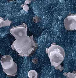
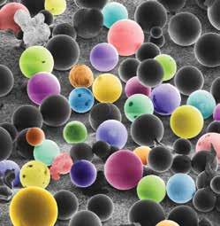
9 Image of mesoporous silica. Nanotechnology researchers are studying mesoporous nanoparticles and their applications in catalysis and drug delivery. Driving Discovery Through Innovative Solutions FEI 7

10 Visualizing atoms and molecules that are involved in chemical reactions and material syntheses is, I think, indispensable. We succeeded in correlating the catalytic activity of gold nanoparticulate catalysts and the structures of gold nanoparticles based on our new methodology that is quantitative ETEM. Professor Seiji Takeda, Institute of Science and Technology, Osaka University, Japan.
11 Chemical Research Powers New Solutions Rising global demand is driving research on materials systems acting as catalysts in industrial chemical processes. Research on catalysts is integral to research on reactive processes such as fossil fuel refinement, substitute natural gas production, base chemical product development, raw material purification, air pollution control, and others. Research focuses on ways to improve catalyst selectivity, activity, and stability. In polymer research, large-molecule composites are specifically assembled (using small-molecule chemical products) to create targeted solutions in almost every imaginable industry. New polymer-based nanosystems contribute to energy savings; aid in the development of new lighting and transistor technologies; enhance the properties of optical, electrical, and biomedical applications; support active sensor controls; enable smart coatings; and advance development of next-generation technologies such as Large-Area Thin-Film Electronics. Polymer research enables innovative compounds that replace existing technologies to reduce costs and deliver new benefits. Innovation demands greater visibility into structures and their functions. What do materials look like and what properties do they exhibit at the nanometer level? How can researchers capture response data while materials are functionalized? What changes occur after a nanosystem is exposed to a range of applied stimuli? These questions make sample preparation, imaging, and analysis more challenging than in the past, and they demand workflows that can deliver high-quality data with integrity and confidence. Driving Discovery Through Innovative Solutions FEI 9
12 Catalyzing Chemical Research Academic and commercial customers alike choose FEI solutions to gain a clearer picture of structural properties, elemental distributions, and dynamic changes at the micro-, nano-, and atomic scales. Powerful FEI Environmental Transmission Electron Microscopes (ETEMs) enable researchers to observe in situ gas-solid reactions and catalysis occurring at the nano- and atomic scale. FEI workflows also provide dedicated experimental chambers for enabling studies in natural conditions and can record reactions for later replay, analysis, and reference. Like FEI ETEM, our Environmental Scanning Electron Microscopes (ESEMs) maintain gaseous environments and provide thermal control. Researchers can reproduce the specific conditions needed for carrying out realistic in situ experiments to explore structure-property-function relationships. For example, scientists can experiment with humidity cycling and in situ wetting, swelling, crystallization, melting, tensile testing, thermal cycling, and more. Integrated high throughput, automated imaging, automated analysis, and connectivity between instruments enables unique experiments and saves time. FEI solutions also provide great flexibility to support a wide range of sample types and experiments for users with varying levels of microscopy expertise. FEI workflows help research progress faster, more easily, and with better-quality results. 10 FEI Explore. Discover. Resolve.

13 13 Chemistry application image with caption TBD Polymer on aluminum substrate Driving Discovery Through Innovative Solutions FEI 11

14 The Super X detection scheme represents an absolute game changer regarding materials research. It has permitted us to make new discoveries regarding well-studied metallic high-entropy alloys, discoveries that previously had been missed. This quality of results allows us to now design new versions of these alloys, with significant commercial advantage regarding their application. Hamish L. Fraser, CAMM and CEMAS, The Ohio State University
15 Understanding the Multiple Dimensions of Metals Metals research has moved to focusing on ever-finer details to drive understanding and innovation. Complete multi-signal, or multi-spectral workflows can deliver unprecedented visibility into grain size, distribution, and composition. Gaining access to this level of detail can be challenging, but it is imperative for improving the value of metals in applications ranging from construction and automotive to aerospace. Metals researchers need a range of visibility into samples from traditional macro and micro visualization down to the micrometer, nanometer, and even atomic levels. They need the ability to clearly understand grain structure and interface chemical composition, which provides insight into the arrangement of grains, precipitates, and interface termination, qualities that relate to material strength, cost, and durability. High-lateral-resolution, highcontrast images, and grain structure spectral information are prerequisites for adapting metal properties to future challenges. In the real-world, metals must also maintain their performance under a huge range of environmental conditions. Using high-resolution imaging, spectroscopy, and diffraction, scientists want to observe the effects of heating, cooling, wetting, freezing, stretching, and straining on a metal s structural morphology in real time. Advanced analysis and visualization tools are essential for progress in metals research. Workflows that enable high productivity and rapid acquisition of the statistically meaningful information are also essential for driving innovation. Driving Discovery Through Innovative Solutions FEI 13
16 Getting Answers From Multiple Scales and Dimensions FEI materials science workflows give researchers powerful, multi-scale characterization capabilities and integrate processes to save time and improve data quality. FEI workflows help customers in a wide range of materials sciences applications, including failure analysis, structural research, sub-nanometer 2D/3D chemical mapping, and optimum distribution of complex chemical compounds in two and three dimensions. Gain high-resolution, high-contrast 2D images on grains, compositions, cracks and other materials features using FEI Scanning Electron Microscopes (SEMs), Focused Ion Beam (FIB) systems, TEMs, and analysis and visualization software. Customers can conduct dynamic 3D volume analysis using FEI SEMs, FIBs, and TEMs with advanced energy-dispersive X-ray and electron diffraction technologies. FEI ESEMs enable scientists to create specific conditions for testing the impact of environmental factors on metals and recording observations as changes occur. And advanced 3D reconstruction, visualization, and segmentation software delivers unprecedented insight into materials characteristics. FEI also offers a range of standalone instruments used in 2D and 3D characterization. Our systems are used around the world for failure analysis, studying microstructure transition, identifying inclusions and precipitates, identifying metals composition, testing corrosion resistance, and visualizing grain distribution and orientation. Whatever the question, FEI provides the workflows and expertise needed to help customers find better answers, faster. 14 FEI Explore. Discover. Resolve.

17 Grain structure in polished steel Driving Discovery Through Innovative Solutions FEI 15
18
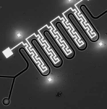
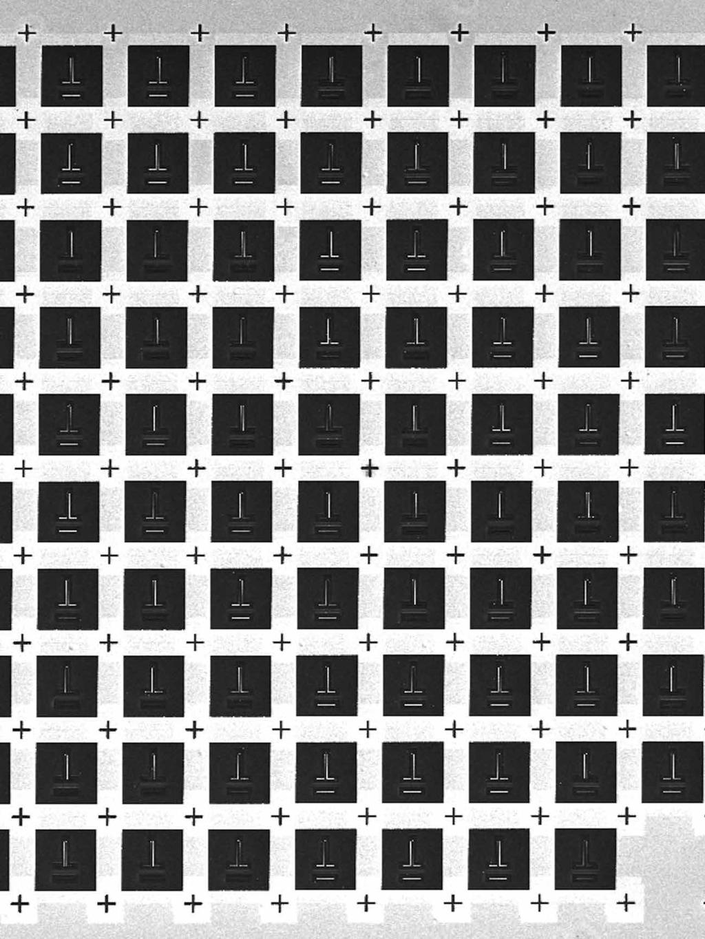
19 Nanodevice Development Challenges the Imagination Nanodevices can be just a few thousand atoms in size and affected by a wide range of physical phenomena. With wide application in a number of areas, the field of nanodevices is an exciting emerging market. With advanced imaging, analysis, and visualization capabilities, scientists can reduce the time that it takes for innovative devices and processes to move from theory to actual commercialization. Nanomaterials offer tremendous opportunity and challenges for researchers. With unique optical, magnetic, electrical and mechanical properties all occurring at the nanoscale these materials have properties that can vary with length scale, changing continuously or instantly. And questions become infinitely more complicated at the nanometer and subnanometer level. How can scientists build prototype devices based on a CAD design when the devices themselves are too small to be seen? What are the ideal substrates for new devices, and how can they be easily manufactured? Validating the functionality of devices this small is also a tremendous challenge. Researchers need to be able to ensure that their prototypes deliver the performance expected using optical, electric, and magnetic stimuli. Although nanodevices may challenge traditional research tools and methods, they become an exciting field of inquiry for customers using FEI solutions. f Array of antennas, minimum feature size <50 nm, written over a 200 x 200 µm 2 field. Image courtesy CIC NanoGune. Driving Discovery Through Innovative Solutions FEI 17
20 No Such Thing as Too Small FEI's device prototyping workflows provide scientists with comprehensive capabilities from CAD design file import for prototyping to characterization of magnetic, mechanical, electrical and optical functionality of final devices. With FEI, it is much easier to correlate function with structure and design at the nanoscale. FEI DualBeam platforms combine SEM and FIB capabilities to deliver the industry s fastest sample preparation times. Unsurpassed resolution and image quality are combined with superior performance for fast imaging and milling. Innovative gas chemistries, detectors, and manipulation technologies enable researchers to create a wide range of structures with unique properties. Capabilities like electron and ion beam deposition and etch assisted with metals or gasses help create innovative substrates and nano structures. In situ and ex situ characterization techniques on FEI platforms enable scientists to quickly validate design and functionality for accelerating product development. FEI solutions can integrate with characterization techniques such as x-ray diffraction, high magnetic field measurements, and others to gain flexibility and deliver unique insights. Researchers can easily apply stimuli to triggers and explore device functionality and performance in a wide range of contexts. With FEI, there is almost nothing that is too small to be developed and explored. 18 FEI Explore. Discover. Resolve.

21 21 Nanodevices application image with caption TBD Surface defects on a solar cell component. Driving Discovery Through Innovative Solutions FEI 19
22 The World is Waiting More efficient energy. Clean steel. Greater safety. Better product longevity. These are just a few of the demands that can be met through the engineering of new and improved materials. As a proven innovator, FEI delivers the data and insight that materials scientists seek with short time-to-answers and in the forms that they need to solve global problems. Our record of microscopy firsts has enabled significant scientific breakthroughs. And we re proud to help our customers be the ones to deliver answers that literally change the world. The First Step Learn more about FEI Materials Science solutions and the work that we are enabling. Visit FEI.com/materials-science and let us help you change the world. 20 FEI Explore. Discover. Resolve.
23 About FEI. With more than 60 years of microscopy innovation and leadership, FEI provides the widest range of electron, ion, and digital light microscopy instrument, workflow, and application expertise in the industry. FEI solutions help customers worldwide answer questions, make breakthrough discoveries, accelerate time to market, and achieve competitive advantage. Rich problem-solving experience from across the electronics, life sciences, materials science, and natural resources markets enables FEI to bring fresh perspectives to customers challenges, whether small and simple or large and complex. FEI people and solutions drive research, propel progress, and ultimately help change the world. About Materials Science. Industry-leading solutions from FEI offer a proven path to results for materials scientists. Our commitment to innovation has resulted in many industry firsts, placing customers at the forefront of advanced research capabilities. With a comprehensive range of flexible workflows to choose from including hardware and software researchers at any level can move from questions to answers quickly and easily. FEI scientists understand customers disciplines, challenges, and goals, enabling them to build long-term partnerships that advance materials research. More customers achieve results and recognition working with FEI than with any other solution provider. Visit FEI.com for more information. Explore. Discover. Resolve.
24 World Headquarters Phone FEI Europe Phone FEI Japan Phone FEI Asia Phone FEI Australia Phone Learn more at FEI.com TÜV Certification for design, manufacture, installation, and support of focused ion- and electron-beam microscopes for the electronics, life sciences, materials science, and natural resources markets We are constantly improving the performance of our products all specifications are subject to change without notice. FEI and the FEI logo are trademarks of FEI Company. All other trademarks belong to their respective owners. BR